Universidade de Aveiro
Departamento de
Electrónica, Telecomunicações e Informática 2013
Telmo Filipe Pedrosa
Cavaco
Compensação da Não-Linearidade do
Modulador-MZ-IQ baseada em FPGA
Compensation of MZ-IQ-Modulator Nonlinearity
Based on FPGA Algorithms
Universidade de Aveiro
Departamento de
Electrónica, Telecomunicações e Informática 2013
Telmo Filipe Pedrosa
Cavaco
Compensação da Não-Linearidade do
Modulador-MZ-IQ baseada em FPGA
Compensation of MZ-IQ-Modulator Nonlinearity
Based on FPGA Algorithms
Universidade de Aveiro
Departamento de
Electrónica, Telecomunicações e Informática 2013
Telmo Filipe Pedrosa
Cavaco
Compensação da Não-Linearidade do
Modulador-MZ-IQ baseada em FPGA
Compensation of MZ-IQ-Modulator Nonlinearity
Based on FPGA Algorithms
Dissertação apresentada à Universidade de Aveiro para cumprimento dos requisitos necessários à obtenção do grau de Mestre em Engenharia Electrónica e Telecomunicações, realizada sob orientação científica do Dr. Paulo Miguel Nepomuceno Pereira Monteiro, Professor Associado do Departamento de Electrónica, Telecomunicações e Informática da Universidade de Aveiro, e do Dr. Rui Fernando Gomes de Sousa Ribeiro, Professor Auxiliar do Departamento de Electrónica, Telecomunicações e Informática da Universidade de Aveiro.
O Júri
Presidente
Vogais
Prof. Dr. José Rodrigues Ferreira da Rocha
Professor Catedrático do Departamento de Electrónica, Telecomunicações e Informática da Universidade de Aveiro
Prof. Dra. Maria do Carmo Raposo de Medeiros
Professora Associada do Departamento de Engenharia Electrotécnica e de Computadores da Universidade de Coimbra
Prof. Dr. Rui Fernando Gomes de Sousa Ribeiro
Professor Auxiliar do Departamento de Electrónica, Telecomunicações e Informática da Universidade de Aveiro
Agradecimentos Gostaria de agradecer à minha família o apoio incansável prestado ao longo da minha formação.
Agradeço também ao Professor Paulo Monteiro e ao Professor Rui Ribeiro por me terem dado a oportunidade de aprofundar conhecimentos na área das comunicações ópticas. Agradeço a orientação e apoio durante a realização da dissertação. Agradeço também ao Professor Arnaldo Oliveira pelos esclarecimentos na área de sistemas reconfiguráveis e ao aluno de doutoramento Ali Shahpari, pela disponibilidade e ajuda nas execuções laboratoriais.
Deixo ainda uma palavra de apreço a todos os meus amigos pelo apoio demonstrado ao longo destes cinco anos.
palavras-chave Comunicações Ópticas, Sistemas de Transmissão Coerente, Modulador Mach-Zehnder, Pré-distorção Electrónica, FPGA
resumo Nos últimos anos, a crescente necessidade de largura de banda e a
evolução das técnicas de processamento digital de sinal renovaram o interesse pelos sistemas de comunicação ópticos coerentes. O modulador IQ assume-se como um componente chave nestes transmissores, sendo responsável pela conversão de informação do domínio eléctrico para o domínio óptico. Os moduladores Mach-Zehnder que constituem este dispositivo recebem sinais de drive com uma excursão controlada, garantindo a utilização de uma região aproximadamente linear das suas funções transferência e a geração de constelações sem distorções de fase. No entanto, existem vantagens em explorar a extensão completa da característica dos moduladores. Neste contexto, torna-se relevante efectuar um estudo acerca das técnicas de pré-distorção electrónica que permitem corrigir os efeitos das não-linearidades associadas a este método de transmissão.
Esta dissertação foca-se no estudo da compensação dos impactos que a característica não-linear do modulador Mach-Zehnder tem nos sistemas de transmissão ópticos coerentes. Após a identificação e desenvolvimento de soluções matemáticas para o problema, realizaram-se vários testes utilizando um simulador integrado em ambiente MATLAB. Um sistema de transmissão coerente utilizando formatos de modulação QAM e os respectivos algoritmos de compensação foram posteriormente implementados em FPGA. Desenvolveram-se também co-simulações que permitiram garantir que o
hardware concebido produzia os resultados desejados. Para além disso, realizaram-se vários testes utilizando um modulador IQ disponível no “Laboratório de Óptica” do Instituto de Telecomunicações de Aveiro. O objectivo consistiu em operar o sistema em condições laboratoriais e analisar o desempenho dos algoritmos de compensação em ambiente real.
keywords Optical communications, Coherent Transmission Systems, Mach-Zehnder Modulator, Electronic Predistortion, FPGA
abstract In recent years, the ever-increasing bandwidth demand and the evolution of digital signal processing techniques renewed the interest for the optical coherent systems. The IQ-Modulator is a key component in optical coherent transmitters, being responsible for the conversion of information from electrical to optical domain. The Mach-Zehnder modulators that compose this device receive driving signals with a controlled excursion, in order to use an approximately linear region of their transfer function and produce constellations without phase distortions. However, there are advantages in exploit the full range of the modulators’ characteristic. In this context, a study about the electronic predistortion techniques required to overcome the nonlinear effects associated to this transmission method becomes relevant.
The subject of this dissertation is the compensation of impairments related to the nonlinear characteristic of the Mach-Zehnder Modulator in coherent optical transmission systems. After the identification and development of mathematical solutions for the problem, several tests were made using a simulator that runs in a MATLAB environment. A QAM coherent transmitter system and the compensation algorithm were then implemented in a FPGA platform. Co-simulations were performed in order to prove that the designed hardware was generating correct results. Furthermore, some tests were conducted using an IQ-Modulator available in the “Optics Laboratory” at Telecommunications Institute of Aveiro. The goal was to operate the system under laboratorial conditions and analyze the performance of the compensation algorithm in a real case scenario.
i
Content
Content ... i
List of Acronyms ... iii
List of Symbols ... v
List of Figures ...vii
List of Tables ... xi
1. Introduction ... 1
1.1 Historical perspective of optical communication systems ... 1
1.2 Historical perspective of Digital Signal Processing in optical communication systems... 2
1.3 Motivation ... 4
1.4 Objectives and dissertation structure ... 5
2. Optical coherent systems ... 7
2.1 The Transmitter: Optical part ... 7
2.2 The Transmitter: Digital part ... 11
2.3 Raised-Cosine filtering ... 12
2.3.1 Intersymbol interference ... 12
2.3.2 First Nyquist Criterion for null ISI... 12
2.3.3 Digital filtering ... 15
2.3.4 FIR filter design: Raised-Cosine response ... 16
2.4 Digital Signal Processing ... 18
2.4.1 Predistortion algorithm ... 21
3. OSIP Simulation ... 25
3.1 Simulation setup and principles of operation... 25
3.2 16-QAM Simulation ... 26
3.2.1 Analysis of the resulting optical spectrum ... 31
3.2.2 Study Case: Constellation’s phase distortions ... 34
3.3 M-QAM Simulations ... 35
4. Hardware implementation ... 39
ii
4.2 Evaluation Kit ... 44
4.3 Implementation of the coherent transmitter system ... 46
4.3.1 Clock generation ... 46
4.3.2 Binary Sequence Generator ... 48
4.3.3 Serial to Parallel Converter ... 49
4.3.4 Coding ... 50
4.3.5 “Phase Flag” Signal Generator ... 51
4.3.6 Upsampler ... 51 4.3.7 Raised-Cosine Filter ... 52 4.3.8 DSP ... 56 4.3.9 DAC Interface ... 62 4.4 Resources utilization ... 68 5. Laboratorial results ... 69 5.1 Co-Simulation ... 69
5.2 16-QAM Laboratorial experiments ... 71
5.2.1 Transmission without Predistortion ... 73
5.2.2 Transmission with Predistortion ... 74
5.2.3 Discussion ... 75
5.2.4 Laboratorial limitations ... 77
6. Conclusions ... 79
6.1 Future work ... 80
7. Appendix 1: VHDL ... 81
8. Appendix 2: Development tools ... 83
8.1 Overview of Xilinx ISE Software ... 83
8.2 Overview of Behavioral Simulation (using iSIM) ... 84
8.3 Overview of Xilinx ChipScope Pro tools ... 85
9. Appendix 3: Test platform ... 87
iii
List of Acronyms
ADC Analog to Digital Converter
ASIC Application Specific Integrated Circuit AWGN Additive White Gaussian Noise
BER Bit Error Rate
BPD Balanced Photodetector
BPF Band-Pass Filter
BRAM Block Random Access Memory
BW Bandwidth
CLB Configurable Logic Blocks CMT Clock Management Tiles
CPLD Complex Programmable Logic Device DAC Digital to Analog Converter
DD Direct Detection
DDR Double Data Rate
DLL Delay-Locked Loop
DQPSK Differential Quadrature Phase Shift Keying DSP Digital Signal Processing
EAM Electro-Absorption modulator EOM Electro-Optic modulator EVM Error Vector Magnitude
FDM Frequency Division Multiplexing FIFO First-In, First-Out
FIR Finite Impulse Response filter
FMC FPGA Mezzanine Card
FPGA Field-Programmable Gate Array HDL Hardware Description Language
HPC High-Pin Count version of FMC connector HSTL High-Speed Transceiver Logic
I2C Inter-Integrated Circuit ICON Integrated Controller
IIR Infinite Impulse Response filter ILA Integrated Logic Analyzer
IM Intensity Modulation
IOB I/O Block
IPCORE Intellectual Property Core
ISE Integrated Software Environment ISI Intersymbol interference
JTAG Joint Test Action Group
LDO Low-Dropout Regulator
LO Local Oscillator
LPC Low-Pin Count version of FMC connector
LPF Low-pass Filter
LUT Look-Up Table
iv LVDS Low-Voltage Differential Signaling
LVPECL Low-Voltage Positive/Pseudo Emitter-coupled Logic
MMCM Mixed-Mode Clock Manager
MZM Mach-Zehnder Modulator
OSA Optical Spectrum Analyzer OSIP Optical Simulator Platform OSNR Optical Signal-to-Noise Ratio PAL Programmable Array Logic PBS Polarization Beam Splitter
PCI Peripheral Component Interconnect PLA Programmable Logic Array
PLD Programmable Logic Device
PM Phase Modulator
PROM Programmable Read-Only Memories
PSK Phase Shift Keying
QAM Quadrature Amplitude Modulation QPSK Quadrature Phase Shift Keying SMA Sub Miniature version A connector SNR Signal-to-Noise Ratio
SPI Serial Peripheral Interface Bus
SPM Self-Phase Modulation
SSTL Stub Series Terminated Logic TDM Time Division Multiplexing UCF User Constraints File
UUT Unit Under Test
VCO Voltage-Controlled Oscillator
VHDL Very High Speed Integrated Circuits Hardware Description Language WDM Wavelength Division Multiplexing
v
List of Symbols
Filter’s coefficients
d Euclidean distance between two adjacent symbols of a constellation
Electrical field at the input of an optical modulator Photodiodes incoming electrical field
Electrical field at the output of an optical modulator
( ) Impulse response of a filter ( ) Transfer function of a filter
( ) Transmitted pulse
Power introduced to the fiber
Power at the output of an optical modulator
Responsivity of the photodiode
, r Bit Rate
, Analog driving signals that will be applied to the electrodes of an optical modulator
Symbol Period Bit Period
( ) External voltage applied to the electrodes of an optical modulator
( ) External bias voltage applied to the electrodes of an optical modulator
Bias voltage applied to the electrodes of an optical modulator
Predistorted analog driving signals that will be applied to the electrodes of an optical modulator
Sum of the voltages applied to an electrode of an optical modulator
Voltage used in a phase modulator
Voltage required by a modulator to invert the electrical field of an optical signal “in-phase” component of the complex envelope of a transmitted signal
“quadrature” component of the complex envelope of a transmitted signal Roll-off factor of the Raised-Cosine filter
Bandwidth that is added to the minimum bandwidth of a ideal low-pass filter Phase shifts in the arms of an optical modulator
vii
List of Figures
Figure 2.1 Phase Modulator ... 7
Figure 2.2 Mach-Zehnder Modulator ... 8
Figure 2.3 Representation of optical power and optical field characteristics as function of the input drive voltage ... 9
Figure 2.4 Optical IQ-Modulator ... 10
Figure 2.5 The Transmitter: Digital part ... 11
Figure 2.6 Transmitter’s structure ... 12
Figure 2.7 Time Domain Representation of the ‘sinc’ function ... 13
Figure 2.8 Frequency Domain Representation of the ‘sinc’ function ... 13
Figure 2.9 Zero Intersymbol Interference ... 13
Figure 2.10 Raised-Cosine: spectrum and impulse response ... 14
Figure 2.11 FIR filter structure ... 16
Figure 2.12 Periodic frequency response of the filter ... 17
Figure 2.13 a) Non-Causal coefficients b) Causal Coefficients ... 17
Figure 2.14 M-QAM constellations ... 19
Figure 2.15 Example of the impact of the MZMs nonlinear characteristic in the generation of multi-level modulation formats ... 20
Figure 3.1 Block Diagram of the Transmitter ... 25
Figure 3.2 Simulation Results: Spectrum after filtering with an ideal filter ... 28
Figure 3.3 Simulation Results: Spectrum of the filtered signal ... 29
Figure 3.4 Simulation Results: Time Domain Representation of the filtered signal ... 29
Figure 3.5 Simulation Results: incorrect 16-QAM constellation for the full excursion ... 30
Figure 3.6 EVM (mean) for different values of “Adaptive Gain” ... 30
Figure 3.7 Simulation Results: Eye Diagram of the IQ-Modulator driving signals ... 31
Figure 3.8 Simulation Results: 16-QAM constellation for unitary “Adaptive Gain” ... 31
Figure 3.9 Simulation Results: Spectrum of the driving signals ... 31
Figure 3.10 Simulation Results: Optical transmitted spectrum ... 32
Figure 3.11 Block Diagram of the transmitter with pre-filtering ... 32
Figure 3.12 Simulation Results: Spectrum of the driving signals after ideal low-pass filtering ... 33
Figure 3.13 Simulation Results: Impacts of the filtering in the resulting optical spectrum ... 33
Figure 3.14 Simulation Results: Impact of the gain in the resulting constellation ... 34
Figure 3.15 Simulation Results: Increase of the constellation’s distortion ... 35
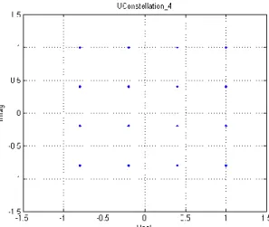
Figure 3.16 Simulation Results: Incorrect 32-QAM Constellation ... 36
Figure 3.17 Simulation Results: Incorrect 64-QAM Constellation ... 36
Figure 3.18 Simulation Results: Correct 32-QAM Constellation ... 36
Figure 3.19 Simulation Results: Correct 64-QAM Constellation ... 36
Figure 3.20 Simulation Results: 32-QAM Optical transmitted spectrum ... 37
Figure 4.1 CLB example for a Xilinx Virtex-6 ... 40
viii
Figure 4.3 Row and Column Relationship between CLBs and Slices in Virtex-6 ... 41 Figure 4.4 Simplified Block diagram of a generic slice ... 41 Figure 4.5 Basic IO Block Diagram ... 42 Figure 4.6 Xilinx Virtex-6 DSP48E1 slice general schematic ... 43 Figure 4.7 Xilinx Virtex-6 Global Clocking architecture ... 43 Figure 4.8 Xilinx ML605 Evaluation Board overview ... 45 Figure 4.9 Simplified Block Diagram of the transmitter system implemented in FPGA ... 46 Figure 4.10 “StoP” for a 16-QAM Coding Block ... 49 Figure 4.11 StoP for a 16-QAM Coding Block: Shift Register ... 49 Figure 4.12 16-QAM Coding Module ... 50 Figure 4.13 16-QAM UpSampler Module ... 51 Figure 4.14 16-QAM Upsampling Process by L=4 ... 52 Figure 4.15 FIR Filter Coefficient file format ... 52 Figure 4.16 16-QAM FIR Compiler Module ... 53 Figure 4.17 Bit Growth for each channel of the FIR Compiler ... 53 Figure 4.18 16-QAM FIR Filter interface ... 55 Figure 4.19 Button Debouncing Block: Simplified schematic ... 55 Figure 4.20 Co-Simulation using the “Test Platform” ... 58 Figure 4.21 16-QAM Constellation after FPGA processing ... 58 Figure 4.22 16-QAM Optical Spectrum after FPGA processing ... 58 Figure 4.23 16-QAM Constellation after FPGA processing, for g=0.4 with 8-bit precision ... 59 Figure 4.24 16-QAM DSP Module Interface ... 61 Figure 4.25 Functional Block Diagram of the AD9963 ... 62 Figure 4.26 Transmit Path Block Diagram ... 63 Figure 4.27 Transmit Path Data Flow and Clock Generation ... 64 Figure 4.28 Transmit Path Timing Diagram ... 64 Figure 4.29 Clock Distribution Diagram ... 65 Figure 4.30 Distorted Square Wave at Evaluation Board’s Output ... 66 Figure 4.31 DAC Interface VHDL Module ... 67 Figure 4.32 DAC Interface Timing diagram ... 67 Figure 5.1 Co-Simulation: Transmitter ... 69 Figure 5.2 Co-Simulation Results: 16-QAM Constellation ... 70 Figure 5.3 Co-Simulation Results: 16-QAM Optical Spectrum ... 70 Figure 5.4 Co-Simulation Results: 32-QAM Constellation ... 70 Figure 5.5 Co-Simulation Results: 32-QAM Optical Spectrum ... 70 Figure 5.6 Laboratorial Setup ... 71 Figure 5.7 Homodyne Coherent Receiver with Phase and Polarization Diversity ... 71 Figure 5.8 16-QAM Constellation for 30% of the full excursion ... 73 Figure 5.9 16-QAM Constellation for excursion... 73 Figure 5.10 Eye Diagram at DACs’ “Q” output for an “Adaptive Gain” of 60% ... 74
ix
Figure 5.11 16-QAM Constellation for 30% of the full excursion ... 74 Figure 5.12 16-QAM Constellation for 80% of the full excursion ... 74 Figure 5.13 16-QAM Constellation for the full excursion ( ) ... 74 Figure 5.14 EVM (mean) for different excursions of the IQ-Modulator driving signals ... 76 Figure 8.1 ISE Design Flow ... 84 Figure 8.2 ChipScope Pro System Block Diagram ... 86 Figure 9.1 Reading Process ... 88 Figure 9.2 Processing Data ... 89 Figure 9.3 Fragmenting Process ... 89 Figure 9.4 SendingProcess ... 90 Figure 9.5 Simplified Block diagram ... 91
xi
List of Tables
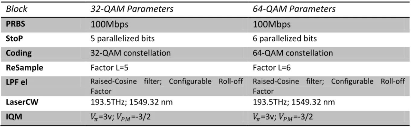
Table 3.1 16-QAM Simulation parameters ... 26 Table 3.2 32-QAM and 64-QAM Simulation parameters ... 35 Table 4.1 Most relevant features of the Virtex-6 FPGA ... 45 Table 4.2 Total hardware usage ... 68 Table 9.1 Total hardware usage by the “Test platform” ... 90
1
1. Introduction
1.1 Historical perspective of optical communication systems
In the 1970s, telecommunication networks were built essentially to carry voice traffic. The few data services that were available over global networks were carried on a voice-optimized infrastructure [1]. However, over the last forty years, the network services have suffered a dramatic change. The number of users has increased exponentially, the available services become more diverse and video is playing an important role in the dominant traffic on network backbones [2]. Traffic growth continues at a rate of almost 50% per year, without showing any signs of slowing [2, 3]. This network capacity increasing was only possible by continued developments in the capacity of fiber optic transmission systems. In the 1970s, the simultaneous availability of compact optical sources (GaAs semiconductor lasers) and low-loss optical fibers (losses could be reduced to 20 dB/km in the wavelength region near 1 µm) led to a worldwide effort for developing these fiber-based systems [4]. Thus, all the progress in these systems can be grouped into several distinct generations.
The first generation became commercially available in 1980 and used GaAs semiconductor lasers for operation near 850 nm, which was a low-loss transmission window of early silica fibers [5]. Those systems operated at 45Mbps, for a single channel, and were based in intensity modulation (IM) at the transmitter and direct detection (DD) at the receiver. They also allowed repeater spacings of up to 10 Km [4,6]. This larger repeater spacing, when compared with the spacing of typical coaxial systems, was an important advantage because it decreased the installation and maintenance costs associated with each repeater [4]. A few years later, the repeater spacing was increased again by moving the operation of the lightwave system to the region near 1300 nm, where the fiber loss is below 1dB/Km and a minimum chromatic dispersion is achieved [4].
The second generation of optical communication systems arose from the need of avoiding the 100Mbps bit rate limitation due to intermodal dispersion in multimode fibers. So, in 1980s, systems began to use single mode fibers and rates of 2 Gbps were achieved [4]. However, the fiber losses were a limitation of these systems, having the typical value of 0.5 dB/km. The solution was to change the lasers wavelength to the region around 1550 nm, where the fiber loss has its minimum [5]. However, this wavelength region has got associated a considerable dispersion. Thus, in order to solve this problem, the third generation of optical communication systems was created. The dispersion problem can be overcome by using dispersion-shifted fibers designed to have minimum dispersion near 1550 nm. Third-generation lightwave systems operating at a bit rate of up to 10 Gbps and with regeneration stages spaced by 70 Km became available commercially in 1990 [4].
The fourth generation is characterized by the invention of the Erbium-Doped Fiber Amplifiers (EDFA) and by the developments in the Wavelength Division Multiplexing (WDM) technology. In a simplified way, it is possible to say that optical amplifiers use a pump laser and a doped fiber to implement the principle of stimulated emission and amplify all the WDM channels contained in a certain spectral region. The WDM technology allowed the transmission of multiple channels simultaneously in a single fiber, which increased the transmission capacity by 10.000 times in twenty years [4]. WDM technology was only possible to develop due to advances in laser manufacturing.
2
Lasers with reduced phase noise and low linewidth have got high spectral coherence, allowing the implementation of coherent optical communication systems [7]. Until then, only IM/DD schemes that respond to changes in the power level of the optical carrier and ignore its phase or frequency content were considered.However, this method does not take full advantage of the bandwidth capabilities of optical fibers. Thus, coherent optical communication systems evolved, treating the light as a carrier medium which can be amplitude or/and phase modulated [5]. This allowed a symbolic representation of the transmitted data and the evolution of advanced data modulation formats. Therefore, an increase in the number of bits that represent each symbol guaranteed higher data rates (and lower symbol rates), resulting in narrower bandwidths. This also reduced the effects of fiber propagation issues and increased the spectral efficiency.
At the same time, two types of modulators were considered: the Electro-Absorption modulator (EAM) and the Electro-Optic modulator (EOM), where the Mach-Zehnder Modulator (MZM) is included (and is going to be explained in the next chapter). An advantage of the Electro-Absorption modulators is that they are made of the same semiconductor material that is used for the laser, and both can be easily integrated on the same chip. However, when compared with all types of MZMs, an EAM has got some disadvantages like low saturation power, large chirp, narrow optical bandwidth and need of temperature control [8]. In 1998, EOMs with a bandwidth of 10 GHz were available commercially [4, 9] and, in 2000s, the bandwidth increased to 40 GHz [9], making the MZMs almost exclusively used for transport systems working at 40Gbps and above. Their main advantages are the well-controllable modulation performance, the possibility of independently modulating intensity and phase of the optical field, broad optical bandwidth and zero or tunable chirp [8].
The fourth generation had also contributed for the development of new systems and fiber concepts that reduce the nonlinear effects caused by the large optical power arising from the presence of many channels in the fiber. New “non-zero” dispersion fibers and some dispersion-management techniques were conceived for this purpose [6]. The fifth generation is concerned with the extension of the wavelength range in which a WDM system can operate simultaneously. The availability of new fibers and Raman amplifiers allowed the operation in 1300-1650 nm with thousands of WDM channels [4].
1.2 Historical perspective of Digital Signal Processing in optical communication systems
All the optical communication systems have got some impairments that must be compensated in order to prevent the degradation of its operation. The earlier compensation techniques arose with the first optical systems and were performed in the optical domain. Those techniques were transparent to the data rate and modulation format of the carried signal, being suitable to systems working at high data rates [10]. For example, dispersion shifted fibers or dispersion compensation fibers were used to reduce the chromatic dispersion. However, this type of compensation was expensive since it uses optical discrete components, giving space to new developments in compensation techniques performed in the electrical domain.3
In recent years, digital signal processing (DSP) techniques have played an important role in optical communication systems evolution, eliminating many problems related to coherent systems. They allow a flexible digital manipulation of data by implementing specific and complex algorithms in high-speed appropriate hardware [11]. Coherent detection with digital signal processing improves receiver sensitivity, spectral efficiency and impairment compensation, increasing the robustness and performance of the system [12]. The transmitter and receiver structures may remain the same regardless of the modulation format. This makes possible to develop flexible transponders that use varying modulation formats depending on the given reach in the system [11, 12].
Digital signal processors are complex integrated circuits that allow complex computations with strict time and accuracy constraints and the implementation of DSP algorithms for coherent optical systems in an efficient way. In 1982, Texas Instruments introduced the first successful “DSP processor”, the TMS32010, which incorporated specialized hardware that enable it to compute a multiplication in a single clock cycle [13]. As might be expected, faster multiplication hardware yields faster performance in many DSP algorithms, and for this reason all modern DSP processors include at least one dedicated single-cycle multiplier or a combined multiply-accumulate (MAC) unit [13]. During 1980s, the developments in CMOS technology and the challenging needs in DSP applications influenced the way DSPs architectures evolved. However, today’s manufacturers have got the same challenges: increase speed, decrease energy consumption, decrease memory usage, and decrease the cost of DSPs [13].
More recently, the “Field-Programmable Gate Array” has been proposed as the technology for DSP systems, since it offers the capability to develop the most suitable circuit architecture for the computational, memory and power requirements of a certain application [14]. Despite being fully described in Chapter 4, an FPGA can be seen as a complex and high speed integrated circuit that provides a method to map logical circuits into hardware. FPGA’s are achieving great performances due to the possibility of parallel execution of multiple operations. Furthermore, FPGA-based designs also offer faster prototyping and the possibility of adapting the hardware during runtime [15].
Before FPGAs started to being developed and becoming viable alternatives in digital signal processing, all the reconfigurable computing technology went through decades of evolution. Before PLDs (Programmable Logic Devices) were invented, PROMs (Programmable Read-Only Memories) were used to store information and create combinational logic circuits. However, PLDs implemented the idea of creating reconfigurable digital circuits, where the combinational function of the device was undefined until its manufacturing time. The PLAs (Programmable Logic Arrays) can be seen as a set of programmable AND gate planes link to a set of OR gate planes, allowing the generation of complex combinational functions. In 1978, PAL (Programmable Array Logic) was introduced by “Monolithic Memories, Inc” [16]. It can be considered an improved PLA, where the OR-plane is fixed and only the AND-plane is programmable [16]. A few years later, some “Complex Programmable Logic Devices” (CPLDs) started to be manufactured. They can be seen as a continuation of the PLA architecture, since the chip includes logic blocks (macrocells) at the borders, and a connection matrix located at the central part. Each macrocell has a structure similar to a PLA. After years of evolution in FPGA technology, their popularity is growing, leading the manufacturers to make an effort to increase
4
their set of features. Reconfigurable computing market segment is leaded by Xilinx, with a share of almost 51% [17]. The remaining competitors are Altera, Actel and Lattice Semiconductor [18]. In 2010, Xilinx released the ‘7’ version of FPGA families, which were built on 28-nm process. The “Virtex” family is optimized for high system performance, with this last version having up to two million logic cells, up to 2.8 Tbps total serial bandwidth, 5.335GMACs, 68Mb Block RAM and even lower power consumption [19,20]. Xilinx also introduced for the first time the “Artix-7” and the “Kintex-7” families which provide better coverage of the lower and mid-end applications previously covered by the “Spartan” family [19, 20]. Altera has made great progress in winning market share in recent years. Their 28-nm FPGAs cover the low, mid and upper end markets with the “Cyclone”, “Arria” and “Stratix” series, respectively [15]. In February 2013, Altera has developed the “Stratix-10”, a new generation of FPGAs manufactured on Intel's revolutionary 14-nm 3D Tri-Gate transistor technology, which can provide, for example, more than ten TFLOPs of single-precision floating-point DSP [21].
Nowadays, due to the standardization of the transmitter and receiver configurations of optical coherent systems, the majority of signal impairments are treated at the receiver, and the algorithms are being implemented using ASICs, DSPs or FPGAs. However, recent researches demonstrate that FPGAs can also be used to generate DSP algorithms at the transmitter [22]. For example, predistorted signals can be generated with the objective that, during the propagation in the transmission channel, nonlinear effects reverse the distortion, resulting in the desired signal waveform at the receiver [22, 23].
1.3 Motivation
In 2000, the ever-increasing bandwidth demand, the increased capacity in WDM systems and the evolution of high-speed digital signal processing renewed the interest for the optical coherent systems [7]. As will be described in the second chapter of this dissertation, the digital information that is transmitted by these systems must be pulse-shaped and converted to continuous-time voltage waveforms, before being applied to the electrodes of an optical IQ-Modulator. This device is responsible for the modulation of an optical carrier and it is composed by two Mach-Zehnder Modulators (MZMs) and a phase-modulator [24]. The MZMs must be biased accordingly to the constellation that it is intended to generate. For example, Square Quadrature Amplitude Modulation (QAM) constellations require the biasing of the modulators in the “Null Point” of their characteristic [25]. Since the optical field response of the MZM is nonlinear, the excursion of the analog driving signals must be reduced and carefully adjusted, in order to use an approximately linear region of the characteristic and produce correctly sized constellations, without phase distortions [26]. Several studies about the impacts of the operating conditions in the transmitted constellations are investigated in [25].
It would be useful to study the possibility of using electrical driving signals that exploit the full modulation depth of the modulators, i.e., that have an excursion equal to the entire range of modulator’s characteristic [26]. This transmission method minimizes the translation of electrical noise into the optical domain in some of the QAM symbols [26, 27]. It also brings benefits in terms of OSNR,
5
since that receiver’s sensitivity can be improved due to a significant performance gain observed for high modulation orders of M-ary QAM constellations [28]. Furthermore, small excursions of the driving signals will lead to a decrease of the optical power efficiency, since the mean optical output power of the MZM will be reduced significantly when compared to its mean optical input power. This will reduce the available OSNR at the receiver side, since the transmit laser power is limited [28].
Despite the increasing of complexity, the inclusion of digital signal processing techniques in the transmitter can be a solution to overcome the nonlinear effects of the IQ-Modulator and allow the use of those higher amplitudes of the ‘I’ and ‘Q‘ waveform data streams [28]. In the past few years, several experiments using transmitter-based electronic predistortion (EPD) were demonstrated, having considerable interest in the compensation of nonlinearities such as self-phase modulation (SPM) or chromatic dispersion [22, 23]. In certain types of experiments, electronic predistortion can bring advantages when compared to receiver-based equalization. One of the reasons is the current availability of commercial high-speed digital-to-analog converters (DACs), while analog-to-digital converters (ADCs) required for the receivers are yet to become generally available [22]. Other important factor is the constant availability of a suitable clock for the DSP circuits at the transmitter without requiring clock recovery. This makes the scheme simpler to implement than receiver-based signal processing [22].
Electronic predistortion can be implemented using ASICs or FPGAs. As seen in the previous section, manufacturers are doing an effort to overcome the processing speed limitation of the FPGAs. Recent advances in several features are enabling their use in optical coherent systems.
1.4 Objectives and dissertation structure
The main purpose of this dissertation is the study of efficient ways of compensating the impairments caused by the nonlinear characteristic of the Mach-Zehnder Modulator in coherent optical transmission systems. The first steps consist in creating OSIP simulations using several QAM formats for development and test of different mathematical solutions. Then, a transmission system that simultaneously performs the compensation algorithm will be implemented in FPGA. The goal is to validate its operation and test the solution under real hardware limitations. This work will be focused in discussing the most efficient solutions, in order to guarantee an increase in the efficiency and a reduction in the hardware requirements.
This document is divided in six chapters. The first one presents a brief historical perspective of optical communication systems and the state of the art of the digital signal processing in coherent systems. In chapter two, details related to the transmission part will be studied. The impacts of the nonlinear characteristic of the Mach-Zehnder Modulator will be analyzed and a solution to compensate those impairments will be discussed. After the conception of an algorithm, the third chapter will present several OSIP simulations, where it is intended to analyze and validate the produced results. In chapter four, some solutions to efficiently implement the transmitter system and the compensation algorithm in a FPGA platform will be discussed. In the fifth chapter, the operation of the system will be tested, in order to assess if the designed hardware is generating proper results.
6
Furthermore, some tests will be performed with the IQ-Modulator available in the “Optics Laboratory” at Telecommunications Institute of Aveiro. The goal is trying to obtain results and get conclusions about the operation of the entire system in real laboratorial conditions. Finally, in the sixth chapter, conclusions and suggestions of possible future work will be presented.
7
2. Optical coherent systems
An optical coherent communication system is one of the most efficient ways to transmit information. It allows a symbolic representation of the transmitted data, enabling the evolution of advanced modulation formats. The increase of the number of bits represented by each symbol guarantees higher rates in signals transmission, since the symbol rates are lower than the corresponding binary rates. This leads to an increased spectral efficiency, with narrower spectral bandwidths.
An optical coherent system consists of a transmitter, a transmission channel and a receiver. The first one is responsible for generating the data and mapping it into a specific constellation. The data will be converted into the optical domain and sent through the transmission channel, where some linear and nonlinear effects will interfere with the signal. The coherent receiver is responsible for the signal´s conversion into the electrical domain and for the information decoding [5]. Generally, digital signal processing is necessary to have a better signal reconstruction, since it was distorted during the transmission.
In this chapter, all aspects related to the transmitter part of an optical coherent system will be discussed. The transmitter has got a fundamental structure composed by an optical and a digital part. In the next two sections both components are going to be studied in order to understand the main concepts related to an M-QAM transmitter system.
2.1 The Transmitter: Optical part
One of the key components of an optical transmitter is the IQ-Modulator. In this section, two fundamental components of the optical modulator will be introduced, providing a better understanding on the IQ-Modulator: the phase modulator (PM) and the Mach-Zehnder modulator (MZM).
In figure 2.1 an optical phase modulator is illustrated. The electrical field of the incoming optical carrier can be modulated in phase simply by applying an external voltage ‘ ( )’, which is going to change the effective refractive index of the optical waveguide [24].
The following expression traduces the transfer function of a phase modulator, where ‘ is the voltage applied to the electrodes needed to generate a phase rotation of :
8
( )
( )
(( )
) (2.1)
In figure 2.2 is illustrated a Mach-Zehnder modulator. It is an external modulator typically used for high capacity systems, essentially due to its superior signal quality when compared with the less performing direct modulation or Electro-Absorption modulators. Furthermore, it provides a smaller frequency chirp, narrower spectrum and higher resilience to chromatic dispersion [29].
In a structural view, it consists of two phase modulators, one on each arm. Thus, the incoming optical carrier is split into two paths. The most commonly used material to fabricate this modulator is Lithium Niobate, which is an electro-optical crystal, whose refractive index also changes in response to an applied electric field. Therefore, the voltages from the modulating signals (‘ ( )’ and ‘ ( ) ) will affect the propagation speed of the light waves. That speed will be higher or lower, depending if the refractive index decreases or increases, respectively. Thus, the two optical fields will acquire a certain phase modulation and will be recombined. Using the principle of interference, the optical fields can interfere in a constructive or destructive way, causing an intensity modulation [24].
Figure 2.2 Mach-Zehnder Modulator
The transfer function of this modulator is given by the sum of two phase modulators transfer functions:
( )
( )
(
( )
( )
)
(2.2)( ) and ( ) are the phase shifts in the upper and lower arms of the modulator. Once again, will be the driving voltage needed to obtain a phase shift of radians on a phase modulator. So, the expressions that relate phase shifts to the driving signals are:
( )
( )
( )
( )
(2.3)
If identical phase shifts are applied in both arms (“push-push” mode), a pure phase modulation is achieved. However, if one arm gets the negative phase shift of the other arm (“push-pull” mode), an amplitude modulation is obtained:
( ) ( ) ( ( ) ( )) ( ) ( ( ( ) ) ( ( ) )) ( ) ( ( ) ) (2.4)
9
By squaring the expression of the output electrical field of the modulator in “push-pull” mode, one may obtain the power transfer function, which is represented in figure 2.3, jointly with the electrical field transfer function:
( )
( )
(
( )
)
(2.5)Figure 2.3 Representation of optical power and optical field characteristics as function of the input drive voltage [24]
By observing the two characteristics it is possible to conclude that the relationship between the modulating signal and the modulator’s output is a nonlinear function.
The typical mode of operation consists in adding a bias voltage to the modulating signal in order to move the region of operation into a range centered in a certain point of the characteristic [24]. Usually, two points of operation are considered:
Quadrature Point: extensively used in direct-detection systems, where the electrical driving voltage is converted into optical intensity.
Null Point: typically used in coherent systems. It corresponds to the point of minimum optical power and it is used because those systems are based in the conversion from electrical driving voltage into optical field.
A multi-level modulation transmission system requires the mapping of bits into symbols from a constellation diagram [29, 30]. Each complex symbol is composed by “in-phase” and “quadrature” components. Thus, the transmitted signal will have the complex envelope ( ) ( ) ( ), where [24]:
( ) ∑
(
)
(2.6)10
Both and represents the “in-phase” and “quadrature” components of the symbol sequence, and is the symbol period. Thus, if one can join two Mach-Zehnder modulators and even add a phase modulator, an optical IQ- Modulator can be created:
Fig 2.4 Optical IQ-Modulator
The IQ-Modulator is often used to create the usually called “Advanced Data Modulation Formats”. The main reason is that with this kind of modulator one can modulate the optical carrier in amplitude and phase, creating data modulation formats as M-QAM (Quadrature Amplitude Modulation with ‘M’ constellation points), M-PSK, etc. These “Advanced Data Modulation Formats” bring benefits in terms of data rates and strength of the optical communications systems, for example. However, as seen in figure 2.3, the nonlinear characteristic of the MZM may be a problem when multilevel modulation data formats are implemented. Later on, solutions for this problem will be discussed.
As illustrated, the incoming electrical field is equally split into two arms: the “in-phase arm” and the “quadrature arm”. In both arms, a field amplitude modulation is performed by operating the Mach-Zehnder modulators in “push-pull” mode. Moreover, a phase shift of is adjusted in one arm, given the possibility of reaching any constellation point in the complex IQ-plane, after recombining the electrical field of the two branches [24]. The transfer function of the IQ-Modulator is [24, 31]:
( (
( )) (
( )))
(2.8)This function proves that signals from both arms are intensity modulated and the signal from the quadrature arm will be also phase shifted by rad. Finally, this transfer function may be re-written in order to include the bias voltages applied to both arms of the modulator:
( (
( )) (
( )))
(2.9)In order to modulate an optical continuous wave carrier produced by the laser, the IQ-Modulator must receive two electrical control voltages with encoded information. Those “driving signals” are generated in the digital part of the transmitter.
11
2.2 The Transmitter: Digital part
This is the part of the transmitter where binary serial data is mapped into specific constellation symbols of the Data Modulation Format that it is intended to implement. Depending on the symbol, two analog voltages will be generated and applied to the IQ-Modulator, allowing the transmission of the information through the optical domain. Therefore, it is necessary to convert the digital processed data into the analog domain. This can be done by using “Digital-to-Analog Converters” [23].
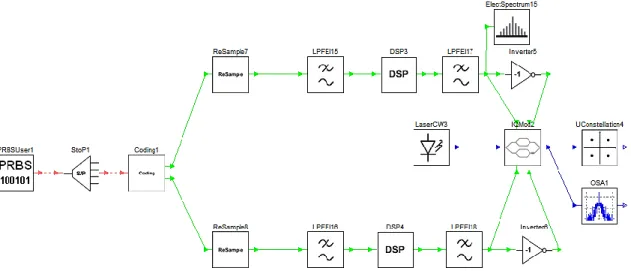
Figure 2.5 The Transmitter: Digital part
The incoming serial binary sequence represents the information that is going to be encoded and transmitted. In this work, pseudo-random binary information will be generated, since the goal is not to transmit any specific information. The “Serial to Parallel Converter” (‘S/P’) will receive the serial information and will parallelize it accordingly to the number of bits required to represent one symbol. The “Coding” block will receive each parallelized word and map it into the corresponding constellation symbol. It will generate two digital voltages, each one representing the projection of the symbol into the ‘I’ and the ‘Q’ axis of the complex IQ-plane. Finally, both DACs will receive digital voltages from the two arms of the transmitter and generate the corresponding analog voltages. It is possible to conclude that only the number of parallelized bits and the conversion of the symbols into two digital representations must be changed accordingly to the Data modulation Format that it is intended to implement.
In this work, more features will be added to the basic digital transmitter structure represented in the figure above. Each output from the “Coding” block can be seen as a “sample” that will be low-pass filtered by a digital implementation of the Raised-Cosine filter. This will allow studying the effects of this pulse shaping filter in the transmitted signal, in particular the spectral occupancy and the improved tolerances to nonlinearities. Furthermore, all the filtered samples will be predistorted in a “DSP” block. There, some mathematical operations will be applied to each sample in order to generate an electronic compensation of the nonlinear characteristic of the MZMs that constitute the IQ-Modulator of the optical part of the transmitter. The goal is to operate the MZMs in the “Null Biasing Point” and obtain non-distorted M-QAM constellations, regardless of the used signal’s excursion. This means that a high-quality data amplifier will be needed to fully exploit the modulation depth of the IQ-Modulator [26].
12
Figure 2.6 Transmitter’s structure
2.3 Raised-Cosine filtering
2.3.1 Intersymbol interference
There are several ways to format binary logic information, in order to transmit it through a communication channel. However, those channels are not perfect, which will cause some signal distortion. If the amplitude and phase responses of a channel are non-ideal, the transmitted pulses will be spread. Intersymbol interference (ISI) occurs when a pulse spreads out in such a way that interferes with adjacent pulses at the sample instant [32].
This type of linear distortion is undesirable in TDM systems because it will cause interference between neighboring pulses. In FDM systems, each multiplexed signal will also be distorted, but no interference occurs with a neighboring channel. This is because each of the multiplexed signals occupies its own band. If the signal spectrums are non-overlapped, no interference occurs between them, since the channel issues will only affect the spectrum of each signal [32].
The main goal is to transmit a pulse at every interval:
( ) ∑
(
)
(2.10) If time-limited pulses are considered, they will not be band-limited, that is, the spectrum will be infinite. Thus, the band-limited communication channel will affect their spectrum and the transmitted pulses will be affected by dispersion effect. The solution is to generate pulses with band-limited spectrums. Despite these pulses are not time-band-limited, there is a way to format them in order to have no intersymbol interference at the sampling instants.
2.3.2 First Nyquist Criterion for null ISI
Nyquist has formulated a criterion which ensures that zero intersymbol interference may be achieved by choosing a pulse shape ( ) with the following response:
( ) { (2.11) The Fourier Transform of ( ) traduces the criterion in terms of frequency domain:
13
The impulse response ( ) may be achieved with the “sinc” function:
( )
( )(
)
(2.13)Figure 2.7 Time Domain Representation of the ‘sinc’ function [32] Thus, the Fourier Transform of a “sinc” function is:
( ) { | |
( )
(2.14) Figure 2.8 Frequency Domain Representation of the ‘sinc’ function [32]
The reason why these pulses cause no ISI is that, at the sampling instants, each one has got a unitary value at its center and a null value at the points where other pulses are centered:
Figure 2.9 Zero Intersymbol Interference [33]
However, a “sinc” pulse is not possible to generate due to its infinite time duration and sharp transition band in the frequency domain, which is physically unrealizable. Furthermore, due to the slow decaying factor of ( ) , ( ), this pulse shape may cause significant intersymbol interference if the received signal is not sampled exactly at the bit instant - small margin for synchronization errors. The solution is to find a pulse that satisfies the equation above, but with a faster time decay and a softer transition in the frequency domain. There is a set of pulses known as “Raised-Cosine” that
14
satisfy the Nyquist criterion and require a slightly larger bandwidth than the “sinc” pulse requires. The spectrum of these pulses is given by [30]:
(
)
{
|
|
[
(
[|
|
])]
|
|
(2.15)where ‘α’ takes values between ‘0’ and ‘1’, and is named as the “roll-off” factor. The impulse response is given by the inverse Fourier Transform:
( )
( ) ( )( )
(2.16)
The following figure intends to illustrate the impulse response and corresponding spectrum. The influence of the “roll-off” factor is also demonstrated:
Figure 2.10 Raised-Cosine: spectrum and impulse response
As shown in figure above, the Raised-Cosine frequency response may be wider than the ideal low-pass filter response shown on figure 2.8, due to the transition band. This additional bandwidth can be adjusted by the “roll-off” factor. This parameter represents the percentage of bandwidth that is added to the defined minimum, or Nyquist, bandwidth. Thus, a null “roll-off” factor originates the ideal low-pass spectrum. On the other hand, if this parameter gets closer to the unitary value, the transition band becomes smoother and the bandwidth becomes higher. Therefore, since the minimum bandwidth is and the maximum is , the following expression can represent the Raised-Cosine bandwidth:
( ) (2.17) The value of the “roll-off” parameter has also consequences in terms of the Raised-Cosine impulse response. A null “roll-off” factor originates a pulse shaping similar to a “sinc” function, since the lobes become higher. However, if the “roll-off” factor gets closer to one, the lobes in the impulse response become smaller, improving the receiver tolerance to timing jitter.
15
Depending on the value of the “roll-off” factor, the impulse response will have different zero crossings. For example, when , the pulse shape will have null values at ( ) , in addition to the usual when [33].
Previously, it was stated that a pulse which satisfies the Nyquist Criterion, but with a faster decay, should solve the intersymbol interference problems due to receiver’s synchronization errors. In fact, as the “roll-off” factor increases, the impulse response goes to zero with a faster decay, and the adjacent lobes become very small. However, the corresponding frequency spectrum may be excessively wide ( ), depending on the applications. Thus, the “roll-off” factor results from a compromise between spectral bandwidth requirements, number of taps of the pulse-shaping filter and receiver sensitivity to intersymbol interference, and should be set depending on the applications [33].
2.3.3 Digital filtering
Ideal filters allow the transmission without distortion of a certain band of frequencies and suppress all the remaining ones. For example, the ideal Raised-Cosine filter (with ) allows all frequencies bellow to pass without distortion and suppresses all the components above . However, many of the ideal filters are physically unrealizable, since they do not satisfy the causal condition [32]:
( )
(2.18) In order to make possible a future hardware implementation of the Raised-Cosine filter, it will be useful to understand how can this filter be generated by a digital implementation.In a generic way, digital filters are easier to design and simulate than the analog ones. They are capable of performance specifications that would be extremely difficult to achieve with an analog implementation. The actual procedure for designing digital filters has the same fundamental elements than the analog filters one’s. First, the desired filter responses are characterized, and the filter parameters are then calculated. Characteristics such as amplitude and phase response are derived in the same way. The key difference between analog and digital filters is that instead of calculating resistor, capacitor, and inductor values for an analog filter, coefficient values are calculated for a digital filter. These numbers reside in a memory as filter coefficients and are used with the sampled data values to perform the filter calculations. However, depending on the operation frequency and the filter specific requirements, digital filters usually require high performance DSP processors and Digital-Analog Converters.
There are two main types of digital filters: finite impulse response (FIR) and infinite impulse response (IIR). For the Raised-Cosine filter implementation, a FIR filter will be considered. Its impulse response has got a finite duration, settling to zero after a certain time. The next figure shows an example of the general structure of an ‘N’ order FIR filter:
16
Figure 2.11 FIR filter Structure
This type of filter is usually composed by multipliers, adders and delay elements, which is particularly useful for hardware implementation. Its output can be defined as a weighted sum of the current and a finite number of previous values of the input:
( ) ∑
( )
(2.19) Where ‘n’ is the sample’s number, ‘ ’ are the filter coefficients, ‘N’ is the filter’s order, ‘ ( )’ is the input signal and ‘ ( )’ is the output signal. One can call to ‘ ( )’ a “filter tap”, where the name has its origins in the discrete taped delay line of digital filter theory. Thus, an ‘N’ order FIR filter generates ‘N+1’ taps [33].The impulse response can be calculated by setting ( ) ( ):
( ) ∑
( )
(2.20) The impulse response ( ) has a finite length, i.e., is non-zero only for a finite range of indices ‘n’. For any FIR filter, ( ) only for . In this case, the filter is also causal [34]. The respective transfer function can be obtained by applying the Z-Transform to the impulse response:
( ) { ( )} ∑
∑
(2.21)
There are also other useful characteristics of FIR filters. One of the most important it is the FIR’s linear phase response. In that case, the impulse response is symmetrical between its left and right side. The location of symmetry has been shifted from zero, which will result in the linear phase, being the slope of the phase’s straight line directly proportional to the amount of the shift. It is also important to notice that a linear phase filter is equivalent to a zero phase filter. The main difference is that a zero phase filter is characterized by an impulse response symmetrical around sample zero. Therefore, the shift in the impulse response simply just produces an identical shift in the output signal [34].
2.3.4 FIR filter design: Raised-Cosine response
Since the frequency response of a digital filter is always periodic in the frequency variable ‘w’ with a period of , the design specifications of the FIR filter need only to be specified for one period, usually, over the frequency region [- , ]. Furthermore, when the frequency response is conjugate-symmetric (i.e. ( ) ( )), then it is enough to specify the response only on the
17
positive frequency interval [0, ]. The conjugate-symmetric case is the most common, because it corresponds to filters with real coefficients [34].
Figure 2.12 Periodic Frequency Response of the filter
The main goal is to design a FIR filter whose frequency response is the same as the Raised-Cosine filter. As seen before, the impulse response of a FIR filter is given by its coefficient values. Thus, the filter coefficients (and consequently, the impulse response) may be calculated by replacing the desired filter parameters in the expression of the impulse response of the ideal Raised-Cosine filter. However, the filter coefficients derived from the expression 2.16 will not produce a causal filter, since they do not satisfy the causal condition previously defined. This means that the system could not be implemented in real time. This can be verified if one considers the output of a discrete-time system produced by the convolution of the input signal with the impulse response coefficients as shown in equation above:
( ) ∑ ( ) (2.22) For example, when , the summation includes a term ( ) that refers to an input value ‘M’ sampling periods behind of ( )’s reference time. The problem can be handled by shifting all coefficient values to the right on the time axis so that only positive values of ‘n’ produce coefficients, as shown in the next figure. The disadvantage of this action is to increase the time delay between system input and output by ‘M’ sampling periods [35]:
Figure 2.13 a)Non-Causal coefficients b) Causal Coefficients [35]
The causal coefficients can be determined from the non-causal coefficients by making some index adjustments. As the non-causal coefficients indices take on values from ‘–M’ to ‘+M’, the causal coefficient indices will take on values from ‘0’ to ‘2M’ [35]:
( )
( )
(2.23)
Furthermore, it is also necessary to guarantee that filter coefficients are symmetric, in order to have a FIR filter with the desired linear phase response [35]:
18
( ) ( ) (2.24) where a non-causal impulse has been considered.
During the filter’s coefficients calculation, and depending on the desired characteristics of the filter, some mathematical indeterminate forms may arise, hindering the proper calculation of these coefficients. One of the multiple ways to solve the problem is to apply the well-known “L’Hôpital’s Rule”. The application (or repeated application) of this mathematical tool allows converting an indeterminate form to a determinate one, ensuring the correct evaluation of the impulse response expression [36]:
( ) ( ) ( ) ( ) ( ) ( )
( ) ( )
( ) ( ) (2.25) Thus, if an indeterminate form of the or type arises, one may derive both numerator and denominator of the expression and then complete the calculations. This technique was useful in the calculations of the filter’s coefficients that were implemented in the experimental part of this work.
2.4 Digital Signal Processing
Before being converted into the analog domain, the filtered samples will be predistorted in the “DSP” blocks. As seen before, Mach-Zehnder modulators have got a nonlinear characteristic. This may be a problem when multi-level modulation data formats are implemented in optical coherent transmission systems. In this section, a solution to compensate the nonlinear response of the modulators is presented.
First of all, it is important to define the QAM data modulation formats. They will be studied in this work because they are widely used in today’s transmission systems and also because they emphasize the MZM’s nonlinearities, due to their multiple amplitude levels.
There are two possible types of QAM constellations: Star QAM and Square QAM. The first one will not be studied since the constellation is not optimal as regards noise performance, because symbols on the inner ring are closer together than symbols on the outer ring. In order to improve noise performance, Square QAM constellations will be generated since they have more balanced Euclidean distances between constellation symbols [24].
QAM modulation formats can be generated by the previously studied transmitter scheme. The signals of both transmitters’ arms represent the “in-phase (I)” and “quadrature-phase (Q)” components of the resulting optical signal. The number of levels of those electrical driving signals is equal to the number of projections of the symbol points into the ‘I’ and the ‘Q’ axis of the complex IQ plane. For example, a Square 16-QAM requires two quaternary driving signals [24].
Depending on the value of the “M”, different constellations may be generated. Below are shown the most common representations of M-QAM:
19
a) 16-QAM b) 32-QAM c) 64-QAM Figure 2.14 M-QAM constellations
It is possible to notice that adjacent symbols are equally spaced by some previously defined distance (‘d’).
QAM increases the transmission´s efficiency, encoding ( ) bits in one symbol, offering higher spectral efficiency than QPSK and reducing the required symbol rate to obtain the same overall bit-rate [26]. However, there are also disadvantages of using this data modulation format. Apart from the higher complexity, QAM also have reduced tolerance towards nonlinearity than QPSK because of the presence of multiple intensity levels and, hence, higher peak-to-average ratio [26]. QAM is also more sensitive to noise (requires an increased OSNR), since the constellation points are much closer, when compared to other modulation formats. Thus, at the receiver, greater accuracy is required for detecting a received symbol. For example, for the same symbol rate, 64-QAM allows transmitting at higher bit rates than QAM because each symbol “encodes” six bits, against the four bits of 16-QAM. However, the 16-QAM Euclidean distance between symbols is greater, allowing detection with fewer errors (greater Quality of Service).
In order to illustrate the impact of the MZMs nonlinear characteristic in the generation of multi-level modulation formats, a simple example is shown below.
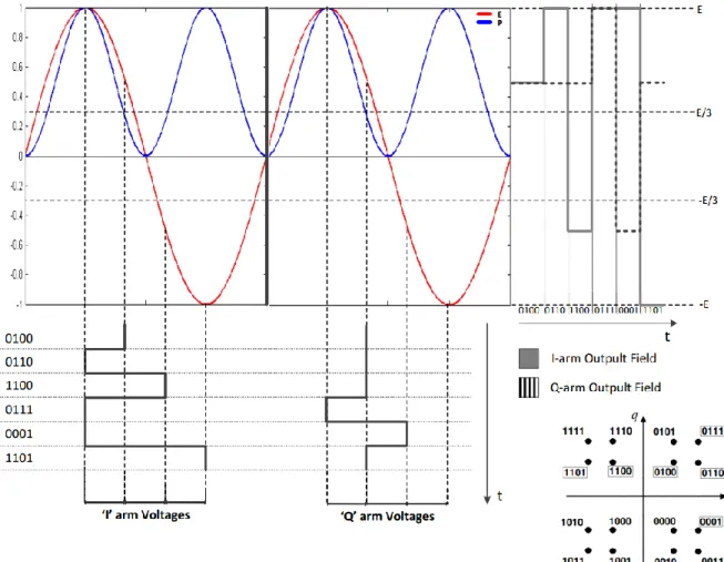
20
Figure 2.15 Example of the impact of the MZMs nonlinear characteristic in the generation of multi-level modulation formats In the example, some random binary data is encoded in six different 16-QAM symbols, which are then converted into the proper analog driving signals and applied to the IQ-Modulator electrodes. The transmitter follows the structure given in the figure 2.6, where the samples are directly converted into the analog domain without any kind of filtering or digital signal processing. The driving signals will be applied to the IQ-Modulator electrodes, modulating an Optical Continuous Wave Carrier.
Accordingly to the constellation shown in figure 2.14-a), it is only possible to represent all the 16-QAM symbols if quaternary driving signals were generated in both arms of the transmitter. The voltage levels of each signal must be equally spaced, respecting the Euclidean distances (‘d’) of a 16-QAM constellation. However, the generation of these driving signals will not result in the expected constellation, since the transfer function of the MZM is nonlinear. Thus, the constellation will come slightly deformed, with unequal Euclidean distances between symbols [25], as can be seen in fig. 2.15. Following the example, the symbols “0100” and “0110” of the resulting optical constellation will be spaced by a Euclidean distance lower than the expected one (‘d’). On the other hand, the symbols “0100” and “1100” will be spaced by a distance greater than ‘d’. These two examples allow explaining the reason why the resulting constellation becomes distorted: due to the nonlinear
![Figure 2.3 Representation of optical power and optical field characteristics as function of the input drive voltage [24]](https://thumb-eu.123doks.com/thumbv2/123dok_br/15939630.1096115/35.918.292.700.206.523/figure-representation-optical-power-optical-characteristics-function-voltage.webp)