Active cellulose-based substrates for application in eletronic devices
286
0
0
Texto
(2) ii.
(3) Diana Filipa Pereira Gaspar Mestre em Engenharia de Materiais. Active cellulose-based substrates for application in electronic devices Dissertação para obtenção do Grau de Doutor em Materiais e Processamento Avançados. Orientador:. Doutor Luís Miguel Nunes Pereira, Professor Associado, Faculdade de Ciências e Tecnologia da Universidade Nova de Lisboa. Co-orientador:. Doutor Rogério Manuel dos Santos Simões, Professor Associado, Universidade da Beira Interior. Júri: Presidente:. Prof. Doutor João Carlos Palma Goes. Arguentes:. Prof. Doutor Henrique Leonel Gomes Prof. Doutora Florinda Mendes da Costa. Vogais:. Prof. Doutor Carlos Pascoal Neto Prof. Doutor Rodrigo Ferrão de Paiva Martins Prof. Doutora Elvira Maria Correia Fortunato Prof. Doutor Francisco Miguel Portela da Gama Prof. Doutor Luís Miguel Nunes Pereira. Julho de 2019. iii.
(4) iv.
(5) Active cellulose-based substrates for application in electronic devices Copyright © Diana Filipa Pereira Gaspar, Faculdade de Ciências e Tecnologia, Universidade Nova de Lisboa.. A Faculdade de Ciências e Tecnologia e a Universidade Nova de Lisboa têm o direito, perpétuo e sem limites geográficos, de arquivar e publicar esta dissertação através de exemplares impressos reproduzidos em papel ou de forma digital, ou por qualquer outro meio conhecido ou que venha a ser inventado, e de a divulgar através de repositórios científicos e de admitir a sua cópia e distribuição com objectivos educacionais ou de investigação, não comerciais, desde que seja dado crédito ao autor e editor.. v.
(6) vi.
(7) Acknowledgments “We must find time to stop and thank the people who make a difference in our lives.” John F. Kennedy The quote that I chose to start my acknowledgements may seem like a cliché, but yet true. During this journey, I had the luck to be surrounded by people that made the difference and supported me during this work and to whom I wish to thank. First, I want to acknowledge my supervisors for their support, advice and guidance. I am profoundly grateful to Prof Luís Pereira, for providing me the scientific knowledge, encouragement, and help that any PhD student needs during this journey. Without his guidance and motivation, this PhD would not have been achievable. My sincere gratitude to Prof. Rogério Simões, for your support, patience, comments during the writing period and knowledge. I know that this thesis is better due to your kind help. Also, thank you for receiving me at UBI (I felt so welcome there!), teaching me so much about paper and to let me make my own paper. I never thought that paper and cellulose could be such an exciting field. I also would like to acknowledge to the colleagues from UBI, Patrícia Baptista, Sónia Sousa, Vera Costa and Prof. Ana P. Costa, that helped me so much and made feel part of the group. To Prof. Rodrigo Martins and Prof. Elvira Fortunato that turned the “paper electronics” a hot-topic, for the shared ideas, fruitful discussions that allowed me to progress, for providing me with the tools and allowing the development of this work in the research facilities of CENIMAT-i3N and CEMOP. Also, I am thankful for the confidence by including me in research projects, which allowed me to evolve personally and professionally. To Prof. Miguel Gama from Minho University that gently offered me bacterial cellulose. A special thank you for Daniela Martins, that had the patience to “feed and take care” of the bacteria in order to produce my special membranes. To Dr David Guerin, from CTP, for providing paper samples and nanocellulose that I studied and tested during this work. To Prof. Maria H. Godinho and Dr Susete Fernandes from Soft Materials Group from FCTNOVA, for the nanocrystalline cellulose membranes that were the beginning of this journey. To Fundação para a Ciência e Tecnologia and AdvaMTech Program for the fellowship (PD/BD/52627/2014). To the European Commission under project NewFun (ERC-StG-2014, GA640598), A3Ple (FP7, NMP-2010-SME-4 grant n° 262782) and BET-EU (H2020-TWINN-2015, GA. vii.
(8) 692373). This work was also supported by the FEDER funds through the COMPETE 2020 Program and the National Funds through the FCT – Portuguese Foundation for Science and Technology. under. the. Project. No.. POCI-01-0145-FEDER-007688,. Reference. UID/CTM/50025, project FunPaper, reference EXPL/CTM-NAN/1184/2013, project PapEl, reference PTDC/CTM-NAN/5172/2014, and project SKINCHIP, reference PTDC/BBB-BIO/1889/2014_LISBOA-01-0145-FEDER-016595. To all my colleagues in the MEON group that, direct or indirectly, contributed to this work: Prof Pedro Barquinha, Prof Rita Branquinho, Prof Joana Pinto, Ing. Alexandra Gonçalves, Ing. Sónia Pereira, Msc. Tiago Mateus, Ricardo Ferreira, Prof. Manuel Mendes, Dr Jonas Deuermier, Dr Asal Kiazadeh, Dr Daniela Gomes, Msc. Tomás Calmeiro, Msc. Jorge Martins (to have so much patience to help me to characterise my devices; I know how that can be challenging), Prof. Ganga Bahubalindruni, Msc. Ana Rovisco, Msc. Emanuel Carlos, Msc. Carolina Marques, Dr Deneb Menda, Dr Ana Pimentel, Msc. João Ribas, Msc. Adriana Costa, Msc. Sara Silvestre and everybody else I don’t have room to mention. Thank you all! I learned so much with you all. A special thank you for my partners of endless clean room work the (1.5 m) girl squad: Msc. Ana Santa, Msc. Cátia Figueiredo, Msc. Inês Martins, and Msc. Maria Pereira. I never get bored around you! To the amazing people that I work every day: Msc. Paul Grey, Msc. Inês Cunha, Msc. Tiago Carvalho, Msc. Raquel Barras, Dr Cristina Gaspar, Msc. Marco Moreira, and Msc.Pedro Claro. It is a great pleasure to share the lab with you! To former colleagues (but lifelong friends) that help and teach me so much in the begging or during this journey: Ing. Nuno Correia, Dr Gonçalo Gonçalves, Dr António Vicente, Dr Andreia Araújo, and Dr Lídia Santos. Also, I would like to extend my gratitude to the administrative support, Sara Oliveira (for the good mood, help and for handling so many issues during this PhD), Sónia Soares, Luís Milhano, Susana Mendes, Valéria Gomes, and Lúcia Mendes. To all my friends for their comprehension and support. To my long(long)time friends Sophie Fidalgo, Rita Fernandes, and Ana Gaspar, for all the friendship, for keeping “centred” in good and bad moments. To Igor and Andreia for the friendship! To Rita and Rodrigo – no words are enough to thank your affection. Finally, to my family for their support, love, for the patience and comprehension during this last year. To my parents who worked very hard to provide me the conditions and opportunities to follow my path. This achievement is also yours!. viii.
(9) Abstract The market for flexible, hybrid and printed electronics systems, which can appear in everything from sensors and wearables to displays and lighting, is still uncertain. What is clear is that these systems are appearing every day in new commercial applications, enabling devices and systems that can, in a near future, be crumpled up and tucked in our pocket. Although the exciting future foreseen for flexible electronics, it is clear that recyclability and sustainability is a concern due to the expected large number of devices to be disposed. This PhD thesis aimed to be part of the (r)evolution of “paper electronics” that targets to turn cellulose into an electronic material, going beyond of considering it just as a substrate for flexible electronic devices. Functional cellulose-based substrates were developed able to serve both as physical support and gate dielectric layer in field-effect transistors (FETs). Several fibre sources were studied and modified aiming to form paper-like membranes with high electric double layer capacitance, enabling highly stable oxide-based FETs and logic gates. A key point is the ionic “doping” of membranes that was achieved either by chemical modification of the pulp or through impregnation of the formed membranes with alkaline solutions. It was found that the ones consisting of small fibres (nanofibrillated or bacterial cellulose) combined with the addition of sodium (Na+) ions result in FETs with low operation voltage (-3 to 3 V), mobility above 10 cm2 V-1 s-1, current modulation surpassing 105 and negligible hysteresis, with proper dynamic response up to 40 Hz. The excellent performance of the FET on cellulose was also possible due to the optimisation of the oxide layers used (IGZO and IZO) as required due to the specific characteristics of fibre-based substrates. One of the innovations brought by this work was on the understanding of the role of hydrogen incorporation in such oxide layers, capable of resulting in optimal electro-optical properties at low deposition temperatures on paper like membranes. The demonstration of electronics on and with cellulose went beyond the implementation as dielectric in transistors. New device architecture was introduced consisting of dual gate planar FETs enabling logic operations making use of just one transistor. This new architecture proved to be useful when integrating other devices, such as photodetectors in the same membrane to control the FETs, proving the enormous potential and versatility of such cellulose-based devices. Keywords: paper electronics; field-effect transistors; cellulose-based FET; electricdouble layer; ionic doping; low temperature.. ix.
(10) x.
(11) Resumo O mercado para sistemas electrónicos flexíveis, híbridos e impressos, que podem surgir em todos os dispositivos desde sensores e wearables a mostradores e iluminação, ainda é incerto. Contudo, o que é certo é que estes sistemas estão a aparecer diariamente em novas aplicações comerciais, possibilitando dispositivos e sistemas que num futuro próximo podem ser dobrados e facilmente guardados num bolso. Apesar do emocionante futuro previsto para a eletrónica flexível, há uma constante preocupação com a sustentabilidade e reciclabilidade devido à grande quantidade de dispositivos que serão descartados. Esta tese de doutoramento ambiciona contribuir para a (r)evolução da eletrónica do papel utilizando a celulose como material eletrónico ativo, e não apenas como um substrato para dispositivos eletrónicos flexíveis. Desenvolveram-se substratos funcionais baseados em celulose que atuam simultaneamente como suporte físico e camada dieléctrica em transístores de efeito de campo (FETs). Foram também estudadas e modificadas diversas fontes de fibras de modo a obter papel com elevada capacidade da dupla camada elétrica, permitindo produzir FETs baseados em óxidos e portas lógicas com elevada estabilidade. Um parâmetro fundamental é a dopagem das membranas com iões alcalinos que foi efetuada com soluções alcalinas, quer por modificação química da polpa quer por impregnação das membranas já formadas. Verificou-se que membranas compostas por fibras menores (nanofibriladas ou celulose bacteriana) quando dopadas com iões sódio (Na+) resultavam em FETs com baixa tensão de funcionamento (-3 V a 3 V), mobilidade acima de 10 cm2 V-1 s-1, modulação de corrente superior a 105, histerese negligenciável, e com uma boa resposta dinâmica até 40 Hz. O excelente desempenho dos FETs em celulose também foi possibilitado pela otimização das camadas de óxidos utilizadas (IGZO e IZO) de acordo com as características específicas dos substratos celulósicos. Uma das grandes inovações deste trabalho foi a elucidação da influência da incorporação de hidrogénio nestas camadas de óxidos que permitiu obter filmes com propriedades eletro-ópticas otimizadas em substratos celulósicos e a baixa temperatura de deposição. A demonstração de eletrónica em e com celulose foi para além da implementação como camada dielétrica em transístores. Foi também implementada uma nova arquitetura consistindo em FETs planares com dois elétrodos de porta, permitindo assim operações lógicas utilizando apenas um transístor. Esta nova arquitetura é extremamente útil quando integrada com outros dispositivos como fotodetectores controlar os FETs, demonstrando o enorme potencial e versatilidade destes dispositivos baseados em celulose. Palavas-chave: eletrónica de papel; transístores de efeito de campo; FET baseados em celulose; dupla camada elétrica; dopagem iónica; baixa temperatura.. xi.
(12) xii.
(13) Contents Chapter 1. Cellulose-based substrates for electronic devices 1.1. Cellulose-based substrates 1.2.. Cellulose. 1.3.. Paper and papermaking process. 1.3.1.. Sources: Raw materials. 1.3.2.. Pulping and papermaking processes. 1.3.3.. Paper classification. 1.4.. Micro/Nanofibrillated and Nanocrystalline cellulose. 1.5.. Bacterial Cellulose. 1.6.. Paper as a substrate for electronics and paper-based devices. 1.6.1.. Thermal and electrical properties. 1.6.2.. Field-effect transistors. 1.7.. ReferencesError! Bookmark not defined.. Chapter 2. Materials and devices: fabrication and characterisation 2.1.. Preparation of the cellulose substrates. 2.1.1. Papermaking process 2.1.2.. Nanocellulose membranes. 2.1.3.. Nanocrystalline cellulose membranes. 2.1.4.. Bacterial Cellulose. 2.2.. Thin films deposition and device fabrication techniques. 2.2.1.. Thin film deposition. 2.2.1.1. Magnetron sputtering 2.2.1.2. Electron-beam assisted thermal evaporation 2.2.2. 2.3.. Field effect transistors. Cellulose substrates and thin-film characterisation. 2.3.1. Structural, morphological, and compositional characterisation 2.3.1.1. X-ray diffraction 2.3.1.2. Porosity 2.3.1.3. Atomic force microscopy 2.3.1.1. Scanning Electron Microscopy. 5 5 5 10 10 11 11 12 15 16 20 21 31 43 43 43 47 48 49 51 51 51 52 53 55 55 55 56 56 58. xiii.
(14) 2.3.1.2. X-ray Photoelectron Spectroscopy 2.3.2.. Optical characterisation. 2.3.2.1. UV-Visible-NIR transmittance spectroscopy 2.3.2.2. Fourier-transform infrared spectroscopy 2.3.3.. Electrical characterisation. 2.3.3.1. Hall Effect 2.3.3.2. Electrochemical Impedance Spectroscopy 2.3.4.. Complementary characterisation techniques. 2.3.4.1. Simultaneous Thermal analysis 2.4.. Electrical characterisation of cellulose-based transistors. 2.5.. References. Chapter 3. Functional oxide thin films 3.1.. Transparent conductive and semiconductor oxides. 3.2.. Hydrogenated TCOs. 3.2.1.. Hydrogenated Zinc Oxide TCOs. 3.2.1.1. Structure and morphology 3.2.1.2. Electrical and optical properties 3.2.1.3. Chemical state and composition 3.2.2. Aluminium-doped zinc oxide and gallium-doped zinc oxide thin films 3.2.2.1. Electrical and optical properties 3.2.2.2. Al and Ga co-doped ZnO thin films 3.2.3.. Hydrogenated Indium Zinc Oxide TCOs. 3.2.3.1. Structure and morphology 3.2.3.2. Electrical and optical properties 3.2.3.3. Electrical properties of IZO:H on different substrates 3.2.3.4. Chemical state and composition 3.3.. Semiconductor oxide thin films. 3.3.1.. IGZO system. 3.3.1.1. Optical and electrical properties 3.3.1.2. IGZO-based FETs 3.4.. xiv. References. 59 60 60 61 62 62 63 64 64 65 67 73 73 76 78 79 82 87 89 90 92 95 96 97 100 101 104 104 105 107 109.
(15) Chapter 4. Transistors on paper-like substrates 4.1.. Substrates from commercial kraft pulp. 4.2.. Influence of the pulp. 4.3.. Fibres’ dimension 4.3.1.. Influence of the water content on the paper’s characteristics. 4.3.2.. Paper/semiconductor interface. 4.3.3.. Influence of the water content in the FETs performance. 4.3.4.. IOn/IOff ratio dependence with frequency. 4.3.5.. Mechanical Stability. 4.3.5.1. Bending tests 4.3.6. 4.4.. Electrical stability over time. Physical modification of bleached softwood kraft pulp (BSKP) papers 4.4.1.. Refining and porosity/density influence. 4.4.2.. FETs on BSKP papers. 4.4.2.1. Influence of the fibres’ orientation 4.5.. Chemical modification 4.5.1.. Addition of extra ionic species to the micro-nanofibrillated cellulose. 4.5.1.1. M/NFC papers: morphology, structure, and electrical characterisation 4.5.1.2. M/NFC papers as a gate dielectric in field-effect transistors 4.5.1.3. FETs stability over time 4.5.2.. Papers produced with TEMPO-mediated oxidised pulps. 4.5.2.1. TEMPO-mediated oxidised papers 4.5.2.2. Influence of the oxidation level in the FETs’ performance 4.6.. References. Chapter 5.Transistors on modified micro/nanocellulose membranes Lightweight micro/nanocellulose membranes 5.1.. Micro/nanofibrillated cellulose 5.1.1.. Micro/nanofibrillated cellulose and influence of the alkaline ion doping. 5.1.1.1. Structural and morphological characterisation 5.1.1.2. Electrochemical characterisation of the NFC-membranes 5.1.1.3. NFC-Membranes as gate dielectric in oxide FETs. 119 119 120 125 125 128 129 132 134 134 136 138 138 141 144 145 146 146 148 150 151 152 153 156 163 163 164 165 165 169 174. xv.
(16) 5.1.1.4. Shelf time stability of the NFC-gated FETs 5.1.1.5. Flexibility, and electrical endurance of the pristine membranes 5.1.1.6. Recyclability 5.2.. 5.3.. 5.4.. Nanocrystalline cellulose 5.2.1.. Structural and morphological properties of NCC membranes. 5.2.2.. NCC-gated FETs. All-cellulose composites 5.3.1.. Structure and morphology. 5.3.2.. All-cellulose composites as gate dielectric in FETs. Bacterial Cellulose 5.4.1.. Alkali-doped BC membranes. 5.4.1.1. Morphological and structural characterisation 5.4.1.2. Application of BC as dielectric in field-effect transistors 5.4.2.. Highly pure membranes and pH influence. 5.4.2.1. pH influence on oxide-based FETs performance 5.5.. References. Chapter 6. Logic operations with transistors on cellulose substrates 6.1.. Dual-gate oxide-based field effect transistors 6.1.1.Architecture and devices’ conception 6.1.2.DG-FGFETs electrical characteristics 6.1.2.1.Influence of the electrodes’ separation and yield of fabrication 6.1.3.Logics in a single DG-FGFET 6.1.4.Tensile Bending Strain Tests. 6.2.. Low voltage logic on NFC membranes 6.2.1.NFC-gated dual-gate transistors 6.2.2.Alkali-doped NFC membranes in inverters. 6.3.. References. Chapter 7. Conclusions and future perspectives 7.1.. Main conclusions. 7.2.. Future perspectives. 7.3.. References. xvi. 177 179 184 187 187 189 191 191 193 195 195 196 199 201 202 203 211 211 212 213 220 223 226 227 228 230 236. 241 241 247 249.
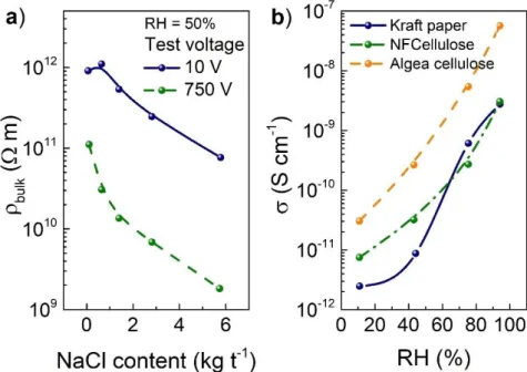
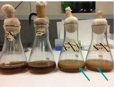
(17) List of Figures Figure 1.1 Schematic association of cellulose at the molecular level in the vegetable cell walls [10], [14]–[16].. 6. Figure 1.2 Scheme of the general structure of the cell wall of fibre, and respective layers (adapted from [17]–[19]).. 7. Figure 1.3 Different cellulose sources in Nature [14], [23]–[26].. 8. Figure 1.4 Cellulose polymorphs (adapted from [11]).. 9. Figure 1.5 From macroscopic fibres to nanomaterials: Top-down approaches for the preparation of micro and nanoscale cellulosic materials [13].. 13. Figure 1.6 a) SEM micrograph of the surface morphology of nanocrystalline cellulose (NCC) membranes obtained from cotton and the corresponding cross section (inset), and b) photograph of the corresponding NCC membrane (adapted from [22]).. 14. Figure 1.7 Bacterial Cellulose - a) Komagataeibacter xylinus micrographs and schematic representation from the extrusion mechanism; b) photograph from a dried membrane, c) SEM image from the membrane’s surface, and d) corresponding cross section [39].. 16. Figure 1.8 a) Bulk resistivity of paper (160 g m-2) as a function of NaCl addition, with RH constant and tested voltages of 10 and 750 V, and b) Conductivity variation with the RH for kraft paper, wood nanofibrillated and algae cellulose (adapted from [88], [90]).. 21. Figure 1.9 Schematic representation of a TFT and a MOSFET [93].. 22. Figure 1.10 Conventional TFT structures depending on the positioning of layers [93].. 22. Figure 1.11 Schematic representation of staggered-bottom gate FETs using cellulose as a gate dielectric.. 23. Figure 1.12 Schematic diagram of the device structure and respective charges modulation for a) oxide-based dielectric and b) EDL in cellulose-based dielectric.. 25. Figure 1.13 Stern model of the electrical double layer at a negatively charged surface.. 26. Figure 1.14 Cross section of an EDL gated devices working in a) electrochemical mode (ECTs), b) field-effect mode, and c) EDL behaviour under a negative and positive V GS, respectively.. 27. Figure 2.1 a) PFI mill in UBI and schematic representation of the working principle. b) Schopper–Riegler apparatus [3].. 44. Figure 2.2 a) Hand sheet former at UBI facilities, and b) dynamic former.. 46. Figure 2.3 a) BBKP and BSEP NFC gel produced at CTP and UBI, respectively. b) NFC dried membranes produced by casting evaporation.. 47. Figure 2.4 Bacterial cellulose fermentation in several bioreactors. The BC slab is identified with the blue arrows.. 50. xvii.
(18) Figure 2.5 Schematic representation of a magnetron sputtering deposition system.. 52. Figure 2.6 Representation of electron-beam assisted thermal evaporation system.. 53. Figure 2.7 Schematic representation of cellulose-based FET deposition steps sequence.. 54. Figure 2.8 (a) Representation of a constructive interference according to Bragg’s Law. b) Panalytical XPert Pro diffractometer at CENIMAT/CEMOP facilities.. 56. Figure 2.9 Asylum MFP3D atomic force microscope system existent in CENIMAT.. 57. Figure 2.10 SEM-FIB Cross-Beam Auriga system existent in CENIMAT facilities.. 58. Figure 2.11 XPS Axis Supra by Kratos Analytical system existent in CEMOP facilities.. 59. Figure 2.12 Thermo Nicolet 6700 Spectrometer equipment used during this work.. 61. Figure 2.13 a) Van der Pauw geometry used for the Hall effect measures. b) Biorad 5500PC Hall effect system installed in the CEMOP.. 63. Figure 2.14 Electrochemical cell produced for the a) potentiostatic, and b) electrochemical impedance spectroscopy. c) Potentiostat 600TM Gamry Instruments used for impedance measurements of the cellulose samples. 64. Figure 2.15 a) Agilent 4155C analyser coupled to a Cascade M150 microprocessor (dark box), and b) microprobe station from Janis Research Company.. 67. Figure 3.1 Periodic table where the elements whose electronic configuration is (n-1)d10s0 are highlighted.. 75. Figure 3.2 Schematic representation of the conduction band for the covalent amorphous (on the left) and ionic semiconductors (on the right), respectively [8].. 76. Figure 3.3 Universal alignment of hydrogen level in semiconductors (adapted from [21]).. 77. Figure 3.4 ZnO thin film growth rate variation as a function of H2 dilution ratio (DH2).. 79. Figure 3.5 a) XRD diffraction patterns of ZnO thin films deposited with different H2 dilution ratios (DH2). The patterns show the preferential growth along [001] directions for the highest DH2.; in the inset the top view of the ZnO crystal for [001] direction is depicted (orange and blue atoms represent O and Zn, respectively). b) and c) detailed view of the (002) reflex shift towards lower 2 values as DH2 increases.. 80. Figure 3.6 Dependence of the crystallite size, and RMS roughness determined by AFM on the H2 dilution (DH2) ratio used. (The lines are guide for the eyes.).. 81. Figure 3.7 SEM micrographs obtained for ZnO thin films for different DH2 tested: a) 0%, b) 0.5%, c) 1%, d) 1.5% and e) 2%, and AFM images DH2 of f) 0 % and g) 1.5 %.. 81. Figure 3.8 Variation of resistivity (ρ) carrier concentration (n), and electron mobility (µ H) for the ZnO films deposited with different H2 dilution ratios (DH2).. 82. Figure 3.9 Optical characterisation of ZnO films processed at different H2 dilution ratios (DH2): a) Optical transmittance spectra. The inset shows the blue-shift of the absorption. 83. xviii.
(19) edge with DH2, b) Linear relation of Eop vs n2/3, corroborating the B-M effect (The line is a guide for the eyes.). Figure 3.10 Dependence of the figure of merit (FoM) on the H2 dilution (DH2). FoM of ITO, FTO, AZO, and GZO are also indicated in the graph using a dashed line only as a guide for the eyes.. 84. Figure 3.11 Temperature dependence of the electrical properties for the ZnO films prepared with DH2 of 0 and 1.5 %: a) Temperature dependence for both µH and n; b) Relation between µH and T for DH2=0 % using the grain boundary (degenerated and non-degenerated) and ionised impurities (non-degenerated) scattering models.. 85. Figure 3.12 Schematic band diagram of the possible electronic transitions responsible for the different emissions in ZnO films.. 86. Figure 3.13 Room temperature PL spectra ZnO films deposited without H2 (dotted line) and with DH2=1.5% (solid line).. 87. Figure 3.14 XPS spectra for films processed without (dashed line) and with H2 dilution (DH2=1.5%, full line): a) ZnO and ZnO:H Zn 2p XPS spectra; b) O 1s Peak from ZnO and ZnO:H.. 88. Figure 3.15 Doped zinc oxide structure, the substitutional position of the doping atoms is represented by the golden atoms.. 89. Figure 3.16 AZO and GZO growth rate variation as a function of H2 dilution ratio (DH2).. 90. Figure 3.17 Electrical properties variation - resistivity (ρ) carrier concentration (n), and electron mobility (µH) - for the a) AZO films, and b) GZO deposited with different H2 dilution ratios (DH2). (The lines are a guides for the eyes.).. 91. Figure 3.18 Influence of the H2 dilution ratios (DH2) on the optical properties of the AZO and GZO films. Optical transmittance spectra of a) AZO, and b) GZO thin films.. 92. Figure 3.19 a) Optical transmittance spectra of AGZO films processed with different power densities; b) Figure of merit (FoM) of the sputtered AZO, GZO and AGZO films in the visible range (solid lines). Reference values of the FoM for ITO, FTO, AZO, and GZO are also indicated in the graph using the dashed line [4].. 94. Figure 3.20 a) XRD diffraction patterns of AZO (5.5 W cm-2), GZO (2.2 W cm-2) and AGZO (5.5/2.2 W cm-2) thin films deposited with DH2=1.5 %, b) and detailed view of the (002) reflex peak. c) SEM micrograph of the AGZO (5.5/2.2 W cm-2) film and respective elementary identification (table).. 94. Figure 3.21 Diffractograms of the sputtered IZO:H films prepared with different D O2 and DH2.. 96. Figure 3.22 a) SEM micrographs of the IZO thin films produced under different sputtering atmospheres (Ar and five different reactive atmospheres), and b) AFM image of the Ar sputtered IZO film.. 97. Figure 3.23 Influence of the deposition conditions on the IZO:H thin films’ electrical parameters: a) resistivity, b) mobility, and c) carrier concentration.. 98. Figure 3.24 a) Optical transmittance of the IZO:H films, and b) Eop as a function of the n2/3,. 99. xix.
(20) according to the Burstein-Moss effect. (The lines are guide for the eyes.) Figure 3.25 Normalised electrical parameters of IZO:H deposited on glass, nanofibrillated cellulose (NFC), sodium-doped NFC (NFC:Na) and commercial standard paper (CSP) with DO2/DH2=1.44%/2.87%.. 100. Figure 3.26 XPS spectra for IZO:H films processed without and with different H2 dilution: 102 a) Zn 2p3/2, and b) In 3d5/2 XPS spectra. Figure 3.27 XPS spectra of O 1s peak for IZO produced under atmosphere of a) Ar, b) Ar + O2, c) Ar + H2, d) and e) Ar + O2 + H2, with DO2(%)/DH2(%) = 1.46/1.46 and 1.42/3.79, respectively.. 103. Figure 3.28 a) XRD diffractograms of the sputtered IGZO 1:2:2 for the different DO2 tested. 105 b) Micrograph and c) AFM 3D topography of the IGZO 1:2:2 produced with DO2=17.6%. Figure 3.29 a) Optical characterisation (optical transmittance and α2-E plots) of the IGZO thin films produced with different O2 dilutions. b) Normalised atomic concentration of zinc, gallium and indium (excluding oxygen) in the IGZO thin films produced with different reactive atmospheres.. 106. Figure 3.30 Arrhenius plot of electrical conductivity dependence as a function of the temperature, used to determine the thermal activation energy the IGZO thin films for the different DO2.. 107. Figure 3.31 Effect of the DO2 on the transfer characteristics of the IGZO FETs on paper annealed at 150 ºC: a) IDS-VGS transfer characteristic, and b) IOn/IOff, S, and VOn.. 108. Figure 4.1 SEM micrographs of samples of a) commercial paper, b) lab prepared softwood pulp substrates and c) lab prepared hardwood pulp substrates.. 121. Figure 4.2 a) XRD diffractograms of samples produced with different pulp sources and b) ATR-FTIR spectra of the different paper samples (normalised to the intensity of the band at 2900 cm−1).. 122. Figure 4.3 Thermogravimetry analysis (TGA and DTA) of the different paper samples.. 123. Figure 4.4 Capacitance variation with frequency (Creal-f) of the three paper samples analysed. The inset shows the structure of the capacitors produced for the EIS measurements.. 124. Figure 4.5 SEM micrographs of a) commercial standard paper (CSP), b) bleached softwood kraft paper (BSKP), and c) micro-nanofibrillated cellulose paper (M/NFC).. 125. Figure 4.6 Electrochemical Impedance Spectroscopy: a) Capacitance variation with frequency (C-f) of the set of paper samples used. (Solid lines represent the capacitance measured at atmospheric pressure, while the open symbols represent the capacitance measured under vacuum after pumping for 15 minutes), b) Phase angle as a function of the frequency, at atmospheric pressure, and c) after under vacuum after pumping for 15 minutes.. 126. Figure 4.7 ATR-FTIR spectra of the bands at 3600-3000 cm-1 and 1635 cm-1 for a) CSP, b) 127 BSKP, and c) M/NFC. The water content variation under vacuum and after recovery was analysed by the changes in the intensity of these bands. d) Thermal analysis of the three different paper samples.. xx.
(21) Figure 4.8 SEM of a cross-section of the paper/IGZO surface. The inset shows an artificial 129 colouration of the IGZO for better visualisation, showing a perfect fibre coverage provided by the sputtered layer. Figure 4.9 Transfer characteristics (IDS-VGS) for the IGZO-based paper FETs on the tested 130 paper samples, and schematic representation of the devices. Figure 4.10 IDS-VGS transfer characteristics of the paper gated IGZO FETs (V DS=15 V) 131 measured initially at atmospheric pressure (solid line), under vacuum after different times and after recovery at atmospheric pressure. Figure 4.11 Gate leakage current (IGS) variation under vacuum conditions and after recovery at atmospheric pressure.. 132. Figure 4.12 IOn/IOff ratio as a function of the applied frequency to the gate of the paper- 133 based FETs (VDS=15 V). Figure 4.13 IDS variation under a square wave of 10 mHz and an amplitude of 40 V (from - 133 20 to 20V). (VDS=15 V). Figure 4.14 Bending test of the paper-based FETs: a) photograph of the devices under test, 135 and normalized electrical characteristics of the devices’ values (µSat - µ/µ0, IOn/IOff ratio I/I0, and S - S/S0) on b) CSP (The inset shows schematic representation of the bending test), c) BSKP and d) M/NFC papers determined under tensile bending strain (solid symbols) and flat position after the bending (open symbols). Figure 4.15 Transfer characteristics (IDS-VGS) of the fresh and four years aged FETs.. 137. Figure 4.16 a) SEM micrographs for the produced BSKP papers, and b) corresponding diffractograms.. 139. Figure 4.17 a) Capacitance as a function of the frequency for the papers produced with a beating index of 27⁰SR and 48⁰SR (solid and dashed lines, respectively), and b) Cole-Cole plots for the papers produced from pulp with 48⁰SR. 141. Figure 4.18 IDS-VGS transfer curves (VDS=15 V) for the FETs produced on the BSKP papers with 27ºSR (on the left), and 48ºSR (on the right).. 142. Figure 4.19 Output curves for the IGZO-FET on calendared orientated paper with a) 27ºSR, and b) 48ºSR, respectively.. 144. Figure 4.20 Preferential orientation of the fibres in respect to the FETs channel: a) schematic representation, b) width-oriented fibres, and c) length-oriented fibres. The dashed lines in b) and c) aim to highlight the fibres’ orientation along the channel.. 144. Figure 4.21 SEM micrographs of the M/NFC papers produced with: a) pristine fibres, 146 b) alkaline pulp (pH=8.5 adjusted with NaOH addition), and c) acid pulp (pH=5.5 adjusted with HCl addition). Figure 4.22 XRD diffractograms for the prepared M/NFC papers.. 147. Figure 4.23 Electrochemical Impedance Spectroscopy of the M/NFC papers. Capacitance and phase as a function of the frequency. The inset shows the Cole-Cole plot to determine the papers’ resistance.. 148. xxi.
(22) Figure 4.24 a) Transfer characteristics IDS-VGS, and b)output curves of the M/NFC gated transistors. In the inset a photograph of the FETs produced with the M/NFC papers is shown (from top to bottom: M/NFC pristine pulp, pulp with pH=8.5, and pulp with pH=5.5).. 149. Figure 4.25 Aging effect of the M/NFC gated FETs: transfer characteristics IDS-VGS of the 150 devices produced on M/NFC with different pH levels. The solid line represents “fresh” devices (1st day), while the dotted line stands for the devices aged for four years. Figure 4.26 Schematic representation of the selective oxidation of mainly the C6 primary 152 hydroxyl groups to C6 sodium carboxylate groups using the TEMPO/NaBr/NaClO system [40]. Figure 4.27 Micrographs of the bleached eucalyptus kraft pulp paper with different oxida- 153 tion levels. a) no oxidation, b) oxidation with 2 mmol of NaClO, and c) oxidation with 4 mmol of NaClO. Figure 4.28 Transfer characteristics of the FETs on BEKP papers with different oxidation grades. On the top right the steps of the preparation of TEMPO-oxidized cellulose and counterion exchange with HCl is depicted.. 154. Figure 4.29 ATR-FTIR data of the BEKP papers with different oxidation grades. The inset shows the full spectra acquired with indication of the zoomed region.. 155. Figure 5.1 Diagram of the top-down approach to obtain cellulose nanofibrils and cellulose nanocrystals.. 164. Figure 5.2 NFC gel produced at CTP (on the left) and UBI (on the right) laboratories.. 163. Figure 5.3 NFC membranes produced with bleached birch kraft pulp (BBKP), and bleached sulphite eucalypt pulp (BSEP), from CTP and UBI, respectively.. 166. Figure 5.4 XRD diffractograms of the pristine and ion enriched BBKP-NFC and BSEP:NFC membranes.. 166. Figure 5.5 FTIR spectra of the pristine NFC and ion doped NFC membranes produced with bleached birch kraft pulp (BBKP – on the left), and bleached sulphite eucalypt pulp (BSEP – on the right).. 168. Figure 5.6 EIS of the BBKP-NFC membranes (pristine, Li, Na and K doped): a) Creal (solid 171 line) and phase angle (open symbols) as function of the applied frequency, b) Comparison of the Creal and Ceff as a function of the applied frequency for NFC:Na, and c) Cole-Cole plot of the NFC membranes. The insets show a zoom of the indicated area for low resistance values from the NFC:Li and NFC:Na. Figure 5.7 Cyclic voltammetry of the BBKP-NFC membranes (pristine, Li, Na and K enriched) at different scan rates.. 173. Figure 5.8 a) Comparison of the capacitances (Creal, Ceff and CDL) obtained from EIS and CV measurements. b) CV of the Al/NFC/IGZO/Al structure produced to emulate the electrochemical behaviour in real FETs for a scan rate = 400 mV s-1. The inset of b) shows a schematic representation of the cells produced to perform the respective measurements.. 174. Figure 5.9 Transfer characteristics (IDS-VGS) with hysteresis of the NFC-gated FETs for. 175. xxii.
(23) VDS = 1 V (on the left) and VDS = 2.5 V (on the right). The scattered squares stand for the IGS. Figure 5.10 Output characteristics for the NFC-gated FETs.. 177. Figure 5.11 Transfer characteristics IDS-VGS of the NFC-gated FETs acquired one day, three months and fifteen months after production.. 178. Figure 5.12 Normalized values of the IOn/IOff ratio (I/I0), sub-threshold slope (S/S0), and 179 mobility (µ/µ0) of the aged NFC-gated FETs. The parameters with the subscript “0” refer to the values determined in the first measurement of the device. Figure 5.13 Normalized electrical parameters of the IOn/IOff ratio (I/I0), sub-threshold slope 180 (S/S0), and mobility (µ/µ0) of the device for outward (on the left) and inward (on the right) bending strains. The open symbols represent the variation of the electrical properties after back to flat condition. Figure 5.14 Transfer characteristic curves of the FETs characterised with a scan rate of 182 0.4 V s-1. On the left the curves for the initial 900 cycles are represented, while on the right the 200 cycles after 8 hours recovery are plotted. The dash-dot lines are indicative of the 1st and 900th cycle of the FET before resting time. Figure 5.15 Electrical performance of the NFC-gated FETs for a scan rate of 4 Vs-1. a) and 183 b) transfer characteristics curves of the initial 900 cycles in semi-log and linear scale, respectively. c) devices behaviour after 8 hours of rest and an extra 200 cycles. d) Normalised On current as a function for the first 900 cycles and the following 200 cycles after an 8h recovering period. e) Leakage current (IGS) variation for the 900 first cycles. Figure 5.16 Normalised electrical parameters (IOn/IOff ratio - I/I0, sub-threshold slope - S/S0, 184 and mobility - µ/µ0) of the devices for 900 cycles (on the left) and 200 cycles after 8 hours of recovery (on the right). The solid symbols represent the scan rate of 0.4 V s-1, and the hollow symbols represent the scan rate of 4 V s-1. Figure 5.17 Steps involved in the NFC FETs recycling process. a) NFC-gated FETs used for the recycling before soaked in water (b1), and b2) after stirring for a few hours. c1) dried pristine and recycled membranes, also photographed in c2).. 185. Figure 5.18 SEM micrograph of the recycled NFC membrane, and EDX elements identification for the Al, In, and Ga. The inset shows an IZO particle with a large dimension entangled in the NFC fibres.. 185. Figure 5.19 a) EIS characterisation of the NFC membranes (pristine and recycled), b) CV of the devices produced to emulate the electrochemical behaviour of real FETs (scan rate=0.4 mV s-1) The inset shows a schematic representation of the produced cells. c) IDSVGS curves of the NFC-gated transistors using pristine and recycled membranes (VGS=2.5 V).. 186. Figure 5.20 Micrographs of the free-standing NCC membranes produced by shear casting 188 (on the left) and by evaporation. The insets show the corresponding cross-sections. Figure 5.21 a) Optical characterisation of the NCC membranes reaching an AVT≈85% 189 (membranes with 30 µm), and b) photograph of one NCC membrane produced by evaporation.. xxiii.
(24) Figure 5.22 NCC-gated FET’s electrical characteristics, a) IDS-VGS transfer and output char- 190 acteristics of the FETs deposited on b) evaporated and c) shear casting NCC. Figure 5.23 SEM images of the all-cellulose composites, NFC and NCC membranes.. 192. Figure 5.24 Specular transmittance of the all-cellulose composites.. 193. Figure 5.25 IDS-VGS transfer characteristics of the FETs with all-cellulose composites as 194 gate dielectrics. Figure 5.26 XRD diffractograms of the BC membranes with different metal alkaline ions.. 196. Figure 5.27 a) SEM Micrographs of the pristine BC and the alkali-doped membranes. b) 197 FTIR spectra of the BC membranes (pristine and alkali-doped). Figure 5.28 Thermal analysis of the reference BC membrane. The thermogravimetric anal- 198 ysis is represented in the left yy axis, and derivative weight is represented in the right yy axis. Figure 5.29 EIS characterisation of the alkali-doped BC membranes: Ceff as a function of the applied frequency (on the left) and determination of the BC resistance (on the right).. 199. Figure 5.30 FETs using alkali-doped membranes as the gate dielectric. On the left the trans- 200 fer characteristics IDS-VGS for a VDS=2.5 V. On the right, saturated output characteristic curves for the FETs on BC:Na. Figure 5.31 a) SEM of pristine BC and of a membrane with pH=11, b) Optical transmittance of the BC membranes with pH=11. The inset shows a photograph of a highly pure dried BC membrane.. 201. Figure 5.32 a) Impedance spectroscopy of the membranes produced with pH=11 showing 202 Ceff and Phase as a function of frequency. b) Transfer (IDS-VGS) curves of the BC-gated FETs (VDS=2.5 V) and c) respective output characteristics. Figure 6.1 a) Schematic illustration of the architecture of IGZO paper DG-FGFETs using 212 the tracing paper as the gate dielectric. G1 and G2 stand for the primary and secondary gate, respectively, while S and D are the source and drain, respectively. Figure 6.2 a) IDS-VGS transfer characteristics of the paper gated IGZO DG-FGFETs at 213 VDS=1 and 15 V (linear and saturation regime). IGS for VDS=1 V and VGS2=0 V is also plotted, b) IDS-VGS transfer characteristics of DG-FGFETs with and without floating gate (VDS=15 V and VGS2=0). Figure 6.3 VON dependence on VGS2, respectively for a VDS of 1V and 15 V. The variation of VON follows a linear tendency that was fitted according to the equations presented in the figure.. 214. Figure 6.4 Comparison of electrical parameters of the paper-based DG-FGFETs for differ- 215 ent VGS2: a) sub-threshold slope (S), and b) mobility (µFE and µSAT) (open symbols for VDS=1 V and solid symbols for VDS=15 V) (The lines are merely guides for the eyes.) Figure 6.5 Schematic representation of the operation mode of the paper DG-FGFETs as a 217 function of the VGS2, and its influence on the accumulation of carriers in the channel, showing the depletion region (in orange). The plots depict the Surface Potential Profile (SPP,. xxiv.
(25) solid lines) for different VGS1/VDS/VGS2 combinations and the resulting Floating Gate potential (VFG) determined for each case (dashed lines). In each situation, a simplified schematic diagram of the ions’ distribution in the paper dielectric is presented, aiming to understand better the potential’s intensity established at the floating electrode that depends on the balance established by VGS1/VDS/VGS2. Figure 6.6 VFG potential simulation using SILVACO software for a DG-FGFETs with 219 VGS1=30 V, VDS=15 V, and VGS2=-5 V, a) Cross-section of the potential profile, b) Surface potential profile at the interface paper/electrodes and respective V FG for the applied voltages, c) Zoom-in of the region near the electrodes, and d) Detail of the potential variation in the IGZO channel. Figure 6.7 a) IDS-VFG transfer characteristics of the paper gated IGZO DG-FGFETs at 220 VDS=1, 6, and 15 V for different VGS2, b) VFG variation as a function of VGS1 and VGS2 for different VDS. Figure 6.8 a) Schematic representation of the separation of the electrodes, and b) respective transfer characteristics for DGFG-FETs for VDS=15V.. 221. Figure 6.9 a) Transfer characteristics for DGFG-FETs with three different distances between S/D and G1/G2 (365, 570, and 770 µm) as a function of VFG, and b) respective variation of VFG with VGS2 as a function of VGS1 (VGS2=[-15;15] V, and VDS=1 V).. 222. Figure 6.10 IDS-VGS transfer characteristics of six IGZO DG-FGFETs at VDS=1 V.. 223. Figure 6.11 Demonstration of a) AND, and b) OR logic in DG-FGFETs on paper substrates with a single device, for an applied frequency of 20 mHz and 40 mHz in VGS1 and VGS2, respectively.. 224. Figure 6.12 Universal logic gates: a) Circuit schematic, b) On-chip implementation, and c) IDS-VGS transfer characteristics DG-FGFETs at VDS=6 V.. 225. Figure 6.13 Dynamic response of the universal logic gates: a) NOR functional demonstration from measurements, and b) NAND functional demonstration from measurements.. 226. Figure 6.14 a) Normalized values of µsat (µ/µ0), ION/IOFF ratio (I/I0) and S (S/S0) for DG- 227 FGFETs determined after measuring the transfer characteristics under tensile bending strain. The bending radius is presented next to the symbols. Solid symbols represent the values calculated for the flat condition after bending. The inset shows a picture of the FETs being measured under bending conditions. b) SEM magnification of the surface of the DGFGFET channel after bending with a tensile strain of 0.75% (equivalent to 5 mm radius). Figure 6.15 a) IDS-VGS curves of the NFC-gated DG-FGFETs with VDS=1 V. b) Voltage 228 output for the a-Si:H PD produced on glass and on NCC in the dark and when irradiated with λ=505 nm. c) Schematic representation of the integration of the DG-FGFETs with the a-Si:H PD. Figure 6.16 IDS-VGS transfer characteristic curves for the DG-FGFETs using an a-Si:H PD 229 produced on glass (on the left) and produced on NCC (on the right) as external bias at VGS2. Figure 6.17 Representation of the integration of a DG-FGFET with an a:Si-H photodetec- 230 tor. Figure 6.18 a) IOn/IOff ratio as a function of the frequency applied to the gate of the NFC- 231 membrane FETs (VDS=3 V). b) Electrochemical characterisation of the NFC membranes xxv.
(26) capacitance and phase as a function of frequency. Figure 6.19 a) Schematic diagram of the inverter. b) Gain as a function of the applied VDD=[1;5] V (on the left) and as function of the load resistance used for a constant VDD=3 V and -3≤Vin≤3 (on the right).. 232. Figure 6.20 Voltage transfer characteristics (VTCs) of the resistor-loaded inverters on NFC measured with VDD=3 V. In the inset the truth table for the logic operations is shown.. 233. Figure 6.21 Voltage output for high and low states of the different NFC based inverters with a fixed VDD (VDD=3 V) and variable load resistances (RLoad=97 kΩ, 561 kΩ and 1 MΩ).. 234. Figure 6.22 Voltage output of the different NFC based inverter with a fixed V DD (VDD=3 V) 235 as a function of the frequency. Figure 7.1 Developments made along this PhD work towards high-performance cellulose- 241 based field-effect transistors. Figure 7.2 Photographs of the several steps involved in the production of the NFC membranes, FETs and final circuits on paper for the IPhO2018.. 246. Figure 7.3 Nature Electronics editorial “A lesson on paper” featuring the IPhO2018.. 246. Figure 7.4 a)Transfer (IDS–VGS) characteristics measured at VDS=1 V for as-deposited devices (solid line) and after 1 minute of O2 plasma treatment to the IZO floating gate, and b) ΔVOn after O2 plasma treatment (VDS of 1, and 15 V) with different VGS2 applied.. 247. Figure 7.5 Schematic representation of reactions occurring between the IZO floating gate and O2 plasma treatment responsible for the VON shift.. 248. xxvi.
(27) List of Tables Table 1.1. Approximate chemical composition of Softwoods and Hardwoods. 10. Table 1.2. Summary of oxide-based transistors using paper as the substrate.. 19. Table 1.3. Comparison of some properties of mature semiconductor technologies.. 24. Table 1.4. Summary of oxide-based transistors using cellulose substrates as a dielectric.. 29. Table 2.1 Paper-like substrates used during this work, and respective details.. 50. Table 2.2 Nanocellulose samples used during this work, and respective details.. 51. Table 2.3. Production details of the cellulose-based FETs layers.. 54. Table 3.1 TCOs materials and some dopants (adapted from [2], [5]).. 74. Table 3.2 Experimental parameters used for the production of ZnO thin films by rf. sputter- 78 ing. Table 3.3 Experimental parameters used for the sputtered doped-ZnO thin films.. 90. Table 3.4 Properties of the AZO and GZO thin films for different sputtering power densities.. 93. Table 3.5 Electrical and optical properties of the AGZO thin films processed at room temperature.. 93. Table 3.6 Deposition conditions of IZO thin films by rf reactive magnetron sputtering.. 96. Table 4.1 Paper-like substrates used during this work, and respective details.. 120. Table 4.2 Characteristics of the paper samples produced with different sources.. 121. Table 4.3 Characteristics of the tested paper samples.. 125. Table 4.4 Summary of the electrical parameters of the IGZO-based paper FETs.. 130. Table 4.5 Dynamic parameters obtained at 10 mHz for paper-based FETs.. 134. Table 4.6 Variation of the electrical parameters of the aged non-encapsulated IGZO-based 137 paper FETs. Table 4.7 Characteristics of the tested paper samples.. 140. Table 4.8 Comparison of the electrical properties of IGZO based FETs for the different 143 BSKP papers tested as a gate dielectric. For the oriented papers, the preferential orientation of the fibres was placed along the width. Table 4.9 Comparison of the electrical properties of IGZO based FETs for BSKP papers with 48ºSR with preferential fibre orientation parallel and perpendicular to the channel.. 145. Table 4.10 Summary of the electrical properties of IGZO based FETs for the M-NCF pa- 149 pers tested as a gate dielectric. Table 4.11 Summary of the electrical properties of aged IGZO FETs for the M-NCF mem- 151. xxvii.
(28) branes tested as a gate dielectric. Table 4.12 Summary of the electrical properties of IGZO based FETs for the BEKP papers tested as the gate dielectric.. 154. Table 5.1 Nanocellulose membranes used during this work, and respective details.. 164. Table 5.2 Properties of the NFC membranes produced with the bleached birch kraft pulp and bleached sulphite eucalypt pulp.. 168. Table 5.3 Summary of the electrochemical and electrical properties of the tested NFCs.. 171. Table 5.4 Electrical properties of NFC-gated FETs for VDS=2.5 V.. 176. Table 5.5 Electrical properties of the FETs with cotton-based NCC as gate dielectric.. 190. Table 5.6 Properties of the all-cellulose composites prepared with the different amount of 193 NFC and NCC Table 5.7 Electrical properties of the FETs with all-cellulose composites as gate dielectrics.. 194. Table 5.8 Summary of the BC membranes’ composition and thickness.. 198. Table 6.1 VFG values obtained for the simplified operation mode of the paper DG-FGFETs 218 as a function of the VGS2 and the ones obtained using SILVACO software and measured.. xxviii.
(29) Acronyms a.c. – alternate current AFM – atomic force microscopy AOS - amorphous oxide semiconductor a-Si - amorphous silicon a-Si:H PD - amorphous hydronated silicon photodetector ATR - attenuated total reflectance ATR-FTIR - Fourier-transform infrared spectroscopy with attenuated total reflectance AVT – average transmittance in the visible range AZO - aluminium‐doped zinc oxide BBKP – bleached birch kraft pulp BEKP - bleached eucalyptus kraft pulp BHKP - bleached hardwood kraft pulp BSEP – bleached sulphite eucalypt pulp BSKP – bleached softwood kraft pulp BC- bacterial cellulose BW – basis weight CEMOP – Centre of Excellence in Microelectronics Optoelectronics and Processes CENIMAT – Centro de Investigação de Materiais CMOS - complementary metal oxide semiconductor CNF – cellulose nanofibrils CNC – cellulose nanocrystals CNT - carbon nanotubes c-Si – crystalline Si CPE - constant phase element CSP - commercial standard paper CTP - Centre Technique du Papier CV - cyclic voltammetry. xxix.
(30) d.c. – direct current DG-FGFETs - dual-gate in-plane oxide-based field effect transistors with a back floating gate electrode DL – diffuse layer DSC – differential scanning calorimetry. ECM - electric circuit model ECT - electrochemical transistors EDL - electric double-layer EDLFET - electric double-layer field effect transistor EGT - electrolyte gated transistors EIS – electrochemical impedance spectroscopy EDX - energy dispersive X-ray spectroscopy FE – field-effect FET – field effect transistor FoM - figure of merit FTIR - Fourier-transform infrared spectroscopy. GZO - gallium‐doped zinc oxide. IC - integrated circuits IGZO –indium gallium zinc oxide IHP – inner Helmholtz plane IS – impedance spectroscopy ITO – indium tin oxide IZO – indium zinc oxide LED - light emitting device. MCC - microcrystalline cellulose M/NFC – micro/nanofibrillated cellulose. xxx.
(31) MOSFET – metal-oxide-semiconductor field-effect transistor MOCVD – metal-organic chemical vapour deposition MWCNT - multiwalled carbon nanotubes. NBE - near band edge emission NCC - nanocrystalline cellulose NFC – nanofibrillated cellulose NIR – near infrared NMOS - n-channel metal oxide field effect transistor NW - nanowire OHP – outer Helmholtz plane OLED - organic light-emitting diode OTFTs - organic thin film transistors. PDMS - polydimethylsiloxane PECVD – plasma enhanced chemical vapour deposition PEN - polyethylene naphthalate PET - polyethylene terephthalate PI – polyimide PL - photoluminescence PMOS - p-channel metal oxide field effect transistor poly-Si – poly-crystalline Si PECVD - plasma enhanced chemical vapour deposition PVD – physical vapour deposition. R-2-R - roll-to-roll manufacturing rf – radio-frequency RFID - Radio-Frequency Identification RH - relative humidity. xxxi.
(32) sccm – standard cubic centimetres per minute SDS - sodium dodecyl sulphate SEM – scanning electron microscopy SPP - Surface Potential Profile STA - simultaneous thermal analysis SWCNT - single-walled carbon nanotubes TCO – transparent conductive oxide TFT – thin film transistor TGA - thermogravimetric analysis TSO – transparent semiconductive oxide. UBI - Beira Interior University UV – ultra-violet Vis. – visible VTC – voltage transfer characteristics XPS - X-ray Photoelectron Spectroscopy XRD – x-ray diffraction ZnO – zinc oxide. xxxii.
(33) Symbols A – optical absorption ⃗ – magnetic field B B-M - Burstein-Moss effect c – speed of light C – capacitance per unit area Cdl – double layer capacitance Ceff – effective capacitance Creal – real capacitance CrI - crystallinity index D – crystallite size dhkl - atomic inter-planar spacing d002 - lattice’s interplanar distance DH2 – H2 dilution DO2 – O2 dilution df – film thickness ds – sample thickness Ea – thermal activation energy EC – conduction band EF – Fermi level Eopt – optical bandgap f – frequency gm – transconductance h – Planck’s constant (4.135×10⁻¹⁵ eV.s) I – current IDS – drain-to-source current IGS – gate leakage current IOn – on current IOff – off current. xxxiii.
(34) IOn/IOff - On/Off current ratio L – channel length n – free carrier concentration Nt - trap density q – elementary charge of a particle (1.6×10⁻¹⁹ C) Q - charge carrier density P – porosity r – radius or radii R – reflectance RH – Hall coefficient RLoad – load resistance Rrms – root-mean-square roughness S – subthreshold swing °SR - Schöpper-Riegler index T – transmittance (%) | temperature (°C, °K) V – voltage VDS – drain to source voltage VFG – potential established along the floating electrode VGS – potential established between the gate electrode and the source VGS1 – primary gate voltage VGS2 – secondary gate voltage VH – Hall voltage VOn – turn-on voltage VTh – threshold gate voltage W – channel width Z – impedance Z’ Zreal – real component of impedance Z’’ Zimag – imaginary component of impedance. xxxiv.
(35) α – absorption coefficient Vhysteresis – FETs hysteresis ε - strain ε0 - vacuum permittivity (8.854×10‐12 F m‐1) η - df/ds ratio, θ – Bragg angle 2θ – angular position κ – dielectric constant λ – wavelength of electromagnetic wave λpl - plasma wavelength µ –mobility µFE –field effect mobility µH –Hall mobility µSat –saturation mobility ν – frequency of electromagnetic wave ρ – electrical resistivity ρcellulose - cellulose density (tabled value: 1.6 g cm-3) ρsample - apparent density of a cellulosic sample σ – electrical conductivity –work function χ - ratio of the film and substrate Young moduli ω - angular frequency ωp - plasma frequency. xxxv.
(36) xxxvi.
(37) Chapter. 1. Cellulose-based substrates for electronic devices. This chapter provides an overview and background regarding cellulose, paper, fieldeffect devices and paper-based field-effect transistors. The contents of Chapter 1 were adapted from the following publications: E Fortunato, D. Gaspar, P. Duarte, L. Pereira, H. Águas, A. Vicente, F. Dourado, M. Gama, R. Martins, Chapter 11 “Optoelectronic Devices from Bacterial NanoCellulose”, in Bacterial Nanocellulose - From Biotechnology to Bio-Economy, 1st ed. Elsevier, 179198, 2016 (DOI: 10.1017/CBO9781107415324.004) A. T. Vicente, A. Araújo, D. Gaspar, L. Santos, A. C. Marques, M. J. Mendes, L. Pereira, E. Fortunato, and R. Martins, Chapter 3 “Optoelectronics and Bio Devices on Paper Powered by Solar Cells,” in Nanostructured Solar Cells, 1st ed. InTech, 33–65, 2017 (DOI: 10.5772/66695)..
(38) Chapter 1. Cellulose-based substrates for electronic devices. 2.
(39) Chapter. Chapter 1. Cellulose-based substrates for electronic devices. 1. Cellulose-based substrates for electronic devices. Chapter 1. Cellulose-based substrates for electronic devices ___________________ 5 1.1.. Cellulose-based substrates ______________________________________ 5. 1.2.. Cellulose _____________________________________________________ 5. 1.3.. Paper and papermaking process ________________________________ 10. 1.3.1.. Sources: Raw materials __________________________________________________ 10. 1.3.2.. Pulping and papermaking processes ________________________________________ 11. 1.3.3.. Paper classification _____________________________________________________ 11. 1.4.. Micro/Nanofibrillated and Nanocrystalline cellulose ________________ 12. 1.5.. Bacterial Cellulose ____________________________________________ 15. 1.6.. Paper as a substrate for electronics and paper-based devices _________ 16. 1.6.1.. Thermal and electrical properties __________________________________________ 20. 1.6.2.. Field-effect transistors ___________________________________________________ 21. 1.7.. References ___________________________________________________ 31. 3.
(40) Chapter 1. Cellulose-based substrates for electronic devices. 4.
(41) Chapter 1. Cellulose-based substrates for electronic devices. Chapter 1. Cellulose-based substrates for electronic devices 1.1. Cellulose-based substrates The interest in lightweight, flexible and low-cost electronic devices has increased in the recent past, pioneering novel applications. One of the major concerns is on the end-oflife and sustainability of devices and materials being used. Polyester-based polymers as polyethylene naphthalate (PEN) or polyethylene terephthalate (PET) stand out as the most common substrates used in large area and flexible electronics mainly due to their mechanical and thermal stability, surface’s morphology (high smoothness), and also being good as an electrical insulator. Although the interesting properties offered by these petrol-based materials, it is clear that recyclable and more sustainable alternatives are necessary for devices aimed to be low-cost and disposable. The use of paper or other cellulose-based substrates as a platform for eco-friendly electronics became a reality in the last years. The ubiquity of paper is unquestionable; this multifunctional material has been for a long time and still is widely used in a variety of applications in our daily life. Thus, thinking of it as part of “green” electronic devices in the future is a legitim ambition. Solid steps were taken during the last decade with the advent of a range of electronic or electrochemical devices manufactured directly onto paper substrates or from cellulose-based functional materials. Some examples are biosensors, energy storage and conversion devices, or even crucial electronic building blocks such as diodes or field-effect transistors, demonstrating that the paper electronics era is establishing its foundations [1]–[6].. 1.2. Cellulose Cellulose is the most abundant natural biopolymer and the elementary building block of paper. In 1838 Anselme Payen isolated it and discovered it is a linear polysaccharide with a repeating unity called cellobiose (Figure 1.1) with the molecular formula [C6H10O5]n [7], [8]. Cellulose consists of a chain with thousands of β (1→4) linked Dglucose units that are covalently bonded through acetal functional groups. This means that the C1 carbon atom1 from one cellobiose is bonded to the C4 carbon of the next unit with a 180° rotation in respect to each other (Figure 1.1) [7], [9]–[11]. 1. Carbon 1 or C1 from each glucose units is commonly denominated as anomeric carbon and is the stereocenter of the acetal functional group.. 5.
(42) Chapter 1. Cellulose-based substrates for electronic devices. Independently of the source, those chains tend to become in parallel assemblies, forming elementary fibrils which can be assembled in bundles with diameters of several nanometres via intermolecular hydrogen bonding between the hydroxyl groups [10], [11]. The ability to form hydrogen bonds confers to cellulose several important characteristics, such as the capability to create a hierarchical organisation with crystalline and amorphous regions, and also important mechanical and physical properties [11]–[13]. The structure of cellulose macromolecules and their hierarchical association in vegetable cell walls is schematically shown in Figure 1.1.. Figure 1.1 Schematic association of cellulose at the molecular level in the vegetable cell walls [10], [14]– [16].. 6.
(43) Chapter 1. Cellulose-based substrates for electronic devices. In vegetal sources, cellulose is obtained mostly from the cell walls; in wood and plant fibres they are organised hierarchically as shown in Figure 1.2. In the middle lamella and primary cell-wall, the cellulose fibrils are short and thin, and its matrix is rich in hemicellulose, structural proteins, and pectin. The secondary cell wall is thicker than the primary one and is formed by three differently structured layers: an outer layer S1, a middle layer S2 and an inner layer S3 (Figure 1.2Figure 1.2) [17]. All the fibrils in each layer run parallel to each other, but all the layers present different directions between them. Besides the higher amount of cellulose, relatively to the primary cell wall, the secondary wall also has hemicellulose reinforced with lignin, which surrounds the cellulose fibrils (Figure 1.2) [7], [18].. Figure 1.2 Scheme of the general structure of the cell wall of fibre, and respective layers (adapted from [17]–[19]).. As mentioned before, besides cellulose other lignocellulosic and non-cellulosic polysaccharides materials can be found in the cell walls structure, namely lignin, and hemicelluloses. Both materials are amorphous, and most of the time it is desirable to. 7.
(44) Chapter 1. Cellulose-based substrates for electronic devices. eliminate them for the papermaking process, although both play an essential role in the cells’ walls. Hemicelluloses are heteropolymers - like xylose, arabinose mannose, galactose, glucose, among others - with low polymerisation degree combined in small noncrystalline chains which can be found in the primary and secondary cell wall and can correspond to 30% of the dry weight depending on the source [17], [19]. Lignin is a three-dimensional macromolecule and considered one of the most resistant materials in nature, which can be found in the cellulose voids in the primary, secondary cell wall, and middle lamella, similarly to hemicelluloses, and its content differs depending on the species. The lignin confers structure and stiffness to the fibre, and also works as a binder, being responsible for holding the fibres gathered in the wood or plants also preventing deterioration of the cellulose [17], [20]. Although the most conventional cellulose’s source in nature are trees and some annual plants as cotton, flax or bamboo, it is possible to find alternative sources in other living beings as cellulose-producing bacteria, algae and fungus-like protists, or even marine animals as the tunicates (Figure 1.3) [8], [11], [21]. The source not only affects the fibril’s length, crystallite size, but also the cellulose’s crystallinity. Bacterial and algal cellulose can present a degree of crystallinity above 80%, while for the vegetal sources as flax or dissolved pulp the crystallinity rounds 50 to 60 %. Furthermore it is possible to reach up to 80% of crystalline fraction for nanowhiskers obtained from cotton [7], [22].. Figure 1.3 Different cellulose sources in Nature [14], [23]–[26].. 8.
(45) Chapter 1. Cellulose-based substrates for electronic devices. Cellulose has four polymorphs: I, II, III, and IV (Figure 1.4). The native one or that found in nature is cellulose I. In its crystalline form the chains are parallelly packed via hydrogen bonding, where each can differ depending on the allomorph, Iα and I [12]. Both polymorphs can occur in the cellulosic materials, and the ratio of the two allomorphs is deeply related to the species. Cellulose Iα is mainly found in cell walls of algae and bacterial cellulose, while the second allomorph is related to vegetable resources such as wood, flax, cotton, and marine animals. The existence of crystalline domains can be assessed by X-ray diffraction, presenting characteristic peaks at 2θ = 14.7°, 16.8° and 22.7° corresponding respectively to the 11̅0, 110 and 200 crystallographic planes of monolithic cellulose type I. The second polymorph, cellulose II (or regenerated cellulose), has an antiparallel chain packaging and is a result of the irreversible re-crystallisation or mercerisation with an aqueous alkali solution of the cellulose I [11]–[13]. Treatment with liquid ammonia of the celluloses I and II lead to the cellulose IIII and IIIII, respectively. Finally, cellulose IV (IVI and IVII) derives from a heating treatment of cellulose IIII and IIIII in glycerol [12].. Figure 1.4 Cellulose polymorphs (adapted from [11]).. 9.
(46) Chapter 1. Cellulose-based substrates for electronic devices. 1.3. Paper and papermaking process 1.3.1. Sources: Raw materials Paper as we know it consists of a matrix of moist pressed fibres, produced mainly from vegetable cellulosic fibres, which can be obtained from wood or other annual plants (e.g. flax, sisal, jute). The last ones are also used for special paper/board grades in some regions of the globe which is commonly defined as nonwood-paper [20]. For the paper used in our daily life for writing, printing or food packaging, for instance, the most common source are undoubtedly the trees; depending on the origin, the fibres can be classified as softwood – from gymnosperm trees, or hardwood – angiosperms trees [27]. The significant differences between those fibres are length, thickness, and chemical composition. Long (> 2-3 mm) and thicker walled fibres are characteristic of softwood species as pine, spruce, and white fir, while smaller fibres with ≈1 mm and thinner cell walls are typical in hardwood trees as oak, birch, and eucalyptus [27]. Those differences extend to the chemical composition of the fibres, tendentially hardwood fibres present higher cellulose/lower lignin grade, in comparison to softwood fibres, while the hemicellulose content is similar for both origins only varying the hemicellulose nature (Table 1.1) [19], [28]. Table 1.1. Approximate chemical composition of Softwoods and Hardwoods (adapted from [19], [28]).. Cellulose Hemicellulose Lignin (*%) (*%) (*%) Softwoods 39-44 15-27 27-32 Hardwoods 38-47 17-30 21-31 * % dry weight The use of softwood or hardwood fibres results in paper with distinct physical and mechanical properties. Long fibres, after beating, usually make dense and strong papers that can be used in liquid packaging boards, carton board and newsprint paper, whereas the short fibres, which are more flexible and easily collapsed, lead to smoother papers with good printability, thus they are widely used to produce tissues and printing paper [20], [27]. Despite the final use of the paper, the choice of softwood or hardwood fibres can also be related to the geographical location, for instance in Scandinavia, spruce is one of the most used sources, while in the south of Europe the eucalyptus is commonly used to obtain paper pulp [24].. 10.
(47) Chapter 1. Cellulose-based substrates for electronic devices. 1.3.2. Pulping and papermaking processes Cellulose fibres from softwood or hardwood origin can be obtained by chemical and/or mechanical pulping processes [9], [30]. The mechanical and thermo-mechanical (woodchips pre-heated) processes act physically, tearing the fibres from each other by application of high shear forces, combined with temperature. The mechanical action leads to a consequent shortening of the fibres keeping the approximate amount of lignin and hemicelluloses present in the wood (20–30%), resulting in a pulp yield above 90 %. Papers formed with this type of pulp generally present low densities due to the highly porous matrix. Since the mechanical pulp results in higher lignin content the paper tends to become brittle over time and yellow with UV exposure [27], [30]. The chemical pulping process involves the “cooking” of raw materials. The fibres are separated by the removal of cross-linked lignin and hemicellulose, using temperature and chemicals. In the kraft (sulphate) process, hydroxide (OH-) and sulphide (HS-) are the active species in cooking. In sulphite processes, different proportions of sulphite (SO32−) and bisulphite (HSO3−) are present, depending on cooking pH [20], [31]. The yield of both processes is substantially lower than the mechanical routes, leading to values between 40 to 50%. After cooking, the pulp fibres are submitted to several (3 to 5) bleaching stages in order to produce the bleached pulp. To produce paper, one or more types of pulps are submitted to a beating process in order to increase fibre flexibility and collapsibility and are mixed with other components, such as fillers and functional additives in a diluted aqueous suspension. This suspension is afterwards subjected to a successive unit operation, mainly sheet forming (including water drainage), pressing and drying. In the drying process, hydrogen bonds between the cellulosic fibres are established, providing the natural resistance to the paper [9], [30]. The extent of beating, the type of pulps, the fillers and the additives are paper grade dependent.. 1.3.3. Paper classification The properties of the paper are deeply related to the fibre’s origin (hardwood or softwood), pulping process, refining extent, fillers, and calendaring; however the most conventional and simple classification adopted to define the paper is based on their weight or grammage [27], [30], [32]. For papermakers and the paper industry it can be roughly defined as tissue - soft and smooth paper with grammage in the range 15–25 11.
(48) Chapter 1. Cellulose-based substrates for electronic devices. g m-2; fine – grammage range from 50–100 g m-2, e.g. office paper; printing –newsprint and magazine paper (40–45 g m-2), and board/packaging – grammage from 100 up to 400 g m-2 [27]. Tobjörk et al., suggested a more straightforward classification dividing the paper into three different categories [30], [32]: •. Light paper: grammage is in the range of 12–30 g m-2, or thickness below 75 µm. In this category two highly transparent, lightweight, and smooth cellulose substrates can be included that are attracting much attention in the recent years: nanocrystalline cellulose (NCC) and bacteria-produced cellulose (BC), that will be described in Section 1.4 and Section 1.5, respectively.. • Standard Paper: includes a wide variety of paper whose basis weight is in the range of 80 to 120 g m-2 and 100 µm thick. Examples for this category are the office paper (80 to 120 g m-2), the translucid parchment paper (~40 g m-2), or even tracing paper (~90 g m-2). Transparent, highly dense and thin papers produced using micro-nanofibrillated cellulose fibres can also be included in this category. Further details about the last will be presented in Section 1.4. •. Cardboard or paperboard: good mechanical resistance and grammage exceeding 200 g m-2, or thickness above 300 µm.. 1.4. Micro/Nanofibrillated and Nanocrystalline cellulose The pulp fibres usually have a high aspect ratio, presenting fibres whose lengths can go up to 4 mm depending on the source, and a width of 20 to 60 µm for hardwood sources or in the range of 30 to 120 µm in the case of softwood [33]. Those fibres can be downsized using a top-down deconstruction to obtain different products depending on the used method and crystalline content. Acid hydrolysis processes lead to microcrystalline bundles and/or nanocellulose crystals (or whiskers), while mechanical ones (with or without enzymatic or chemical treatments) lead to cellulose micro and nanofibrils. (Figure 1.5) [12], [13], [34]. The terminology for the so-called micro and nanofibrillated cellulose (M/NFC) is not clearly established leading to some misunderstandings. Other designations, such as cellulose microfibrils and nanofibrils, fibrillated cellulose, nanofibrillar cellulose, microfibrillated cellulose nanofibers, among others, refer to refined cellulose microfibrils with monocrystalline and amorphous regions, which are composed of nanosized fibrils with 5 to 100 nm of width and few µm in length, leading to a high 12.
Imagem

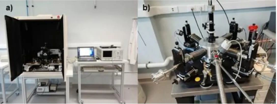
![Figure 2.1 a) PFI mill in UBI and schematic representation of the working principle. b) Schopper–Riegler apparatus [3]](https://thumb-eu.123doks.com/thumbv2/123dok_br/18155067.872337/80.892.179.682.564.931/figure-schematic-representation-working-principle-schopper-riegler-apparatus.webp)

+7


Documentos relacionados