Miguel Alexandre Martins Franco
Licenciado em Engenharia de Micro e NanotecnologiasResistance Switching Memory
Devices based on Zinc Oxide
Nanoparticles on Paper Substrates
Dissertação para Obtenção do Grau de Mestre em Engenharia de Micro e Nanotecnologias
Orientador: Doutor Luís Miguel Nunes Pereira, Professor Auxiliar, Faculdade de Ciências e Tecnologia da Universidade Nova de Lisboa
Co-orientadora: Doutura Asal Kiazadeh Professora Auxiliar, Faculdade de Ciências e Tecnologia da Universidade Nova de Lisboa
Júri
Presidente: Doutor Rodrigo Ferrão de Paiva Martins, Professor Catedrático, Faculdade de Ciências e Tecnologia da Universidade Nova de Lisboa
Arguente: Doutora Joana Maria Dória Vaz Pinto, Professora Auxiliar, Faculdade de Ciências e Tecnologia da Universidade Nova de Lisboa
Vogal: Doutor Luís Miguel Nunes Pereira, Professor Auxiliar, Faculdade de Ciências e Tecnologia da Universidade Nova de Lisboa
Resistance Switching Memory Devices based on Zinc Oxide
Nanoparticles on Paper Substrates
© Miguel Alexandre Martins Franco
Faculdade de Ciências e Tecnologia
Universidade Nova de Lisboa
Resistance Switching Memory Devices based on Zinc Oxide Nanoparticles on Paper Substrates
I
ACKNOWLEDGMENTS
I want to thank the people that doesn’t respect me, constantly trying to destabilize me and even worse, thinking that I am an unconscious person who dedicates and help them. Sorry to say, but I will give bad news to these people. Despite of being a dedicate and helpful person I’m not blind and I hate when people try to foul me. Their attempts to cause my failure are just a force and a motivation to follow my dreams. Probably these lines that I have dedicated in this work won’t be read for who wanted to possess my feelings and make my life a beautiful lie. I won’t provide the names of these people because I respect these people despite the damage taken. They are now ghosts haunting in my head, screams from the past that I remember today.
I have dreams. I fight for them. My imperfections and failures are my motivation to be a better person. I want to be improve to reach perfection. When I reach the utopia it will be my doom. Perfection means the end of a journey, the end of a life. With perfection the motivation banishes along the air that I need to live.
I want to live in a better world. I want to ensure the next generations have a green planet to live, preserve and respect. I want to live in a planet where everyone is conscious and aware the problems and challenges. This is my wishes, this is my thoughts when I throw a coin into the bottom of a well, when I’m looking to a shooting star, aware the situation won’t be changed by wishing and wait for other to do and fight. I became frustrated and disappointed to watch the situation of this condemned civilization. People only worries about his commodity, ignoring the real problems that could ruin the prosperity of our society. People are enslaved with gadgets, like kittens playing with a rope while some influent people easily manipulates with two objectives: power and money. I start to became worried because our society are numb and ignorant. I see a Europe full of good ideals being corrupted by lobbyists, causing the inevitable destruction process of a utopic European Union of a disunited members and lost voices.
I’m here trying to make the world a better place to live. This is the reason I’ve entered to Micro and Nanotechnology Engineering at FCT-UNL. I wanted to expand my knowledge, to learn the tools needed to the search of knowledge. Five years have passed and I’m one step to be graduated. It was a privilege to be able to integrate in a creative and prestigious team like CENIMAT|i3N and CEMOP, for me a worldwide pioneer in paper electronics. A restless demand in order to overcome barriers and open new horizons in scientific knowledge are a constant in these centres, developing innovative, challenging and current work applied in different areas. Therefore, first of all I would like to thank Professor Rodrigo Martins and Professor Elvira Fortunato for the access to these installations and technology. Their multidisciplinary knowledge, competence and commitment allow the excellent conditions of work here in CENIMAT|i3N and CEMOP. In addition, I would like to thank for the fact of being able to open this unique and outstanding integrated masters in Portugal.
Secondly, I would like to express my sincere gratitude to my supervisor, Professor Luís Pereira for accepting and give me the chance to join and work in his research group. I cannot thank you enough for all support, encouragement, valuable suggestions, availability and the spirit of research, your inspiring enthusiasm. I am also grateful for all the support given by his extraordinary group of researchers including Tiago Carvalho, Paul Grey, Inês Cunha, Diana Gaspar, Raquel Barras and Pedro Freitas. For all the advices, knowledge, the inspiring long hours of hard-working spent in the. Thank you for always finding time to discuss the things that you guys well know. Once again, thank you Tiago for your relevant and innovative suggestions and for always find time to help in every possible way. Essentially, thanks to all of you and especially to Professor Luís for installing this team and work spirit.
In order to not forget anyone, I would like to express my gratitude to the rest of these both institutes for the support and the relevant suggestions.
Also, I am a grateful to my colleagues and course mates of Micro and Nanotechnology and Materials Science as well. Thanks for the support with the tasks from those different areas during this degree.
Resistance Switching Memory Devices based on Zinc Oxide Nanoparticles on Paper Substrates
II
Resistance Switching Memory Devices based on Zinc Oxide Nanoparticles on Paper Substrates
III
ABSTRACT
This work reports the development of resistive random access memory (RRAM) on paper using printed Zinc Oxide (ZnO) nanoparticles (NPs) as active layer. RRAM is a novel technology having attracted increasing attention due to their high-speed operation, high-density storage, and low voltage. Most important, due to its characteristics it could replace flash technology which suffers from low endurance, low write speed, and high voltages required for the write operations.
Screen printing was chosen because of its versatility in terms of ink viscosity, which is compatible with inks that require low annealing temperatures. The architecture adopted consists in a mixture of ZnO NPs and ethyl cellulose (EC), used as binder, between electron beam evaporated platinum bottom electrode and screen-printed carbon or silver top electrode.
The resistive memory device can be programed in bipolar for at most 20 cycles. The retention time of the bipolar switching for both on/off states is reached up to 10 Ks. The operating voltages of SET and RESET is high ~ 20 V and - 10 V respectively. A transition between bipolar switching to unipolar is observed. It is suggested that an instable bipolar resistive switching is due to growth of filaments during cycles. The required voltages for on/off states fluctuate in the range of ~ 5 V which is a strong evidence of non-consistent bipolar resistive switching.
Keywords: Zinc oxide, ethyl cellulose, paper electronics, resistive random access memory,
Resistance Switching Memory Devices based on Zinc Oxide Nanoparticles on Paper Substrates
Resistance Switching Memory Devices based on Zinc Oxide Nanoparticles on Paper Substrates
V
RESUMO
Este trabalho reporta o desenvolvimento das memórias resistivas em substrato de papel usando nanopartículas (NPs) de óxido de zinco (ZnO) e de etilcelulose (EC), como camada ativa. As memórias de acesso aleatório resistivas (RRAM) são uma tecnologia recente que tem atraído crescente atenção devido á rápida velocidade de operação, alta densidade de armazenamento e baixa temsão de funcionamento. Devido ás suas características poderão substituir a memoria flash que tem como limitações a baixa endurance, baixa velocidade de escrita e altas voltagens para escrever.
A técnica de screen printing foi escolhida devido a sua versatilidade em termos da viscosidade da tinta, que torna compatível a criação de tintas que requerem baixa temperatura de recozimento. A arquitetura adotada consiste numa mistura de nanopartículas de óxido de zinco envolvidas em etilcelulose entre contato inferior de platina depositado por evaporação por canhão de eletrões e contato de topo de carbono ou de prata impresso por screen printing.
As memorias resistivas podem ser programadas no modo bipolar até 20 ciclos. O tempo de retenção atingido após transição bipolar para ambos os estados on e off foi de 10 000 segundos. A tensão de operação de SET and RESET é elevado ~20 V e -10 V respetivamente. A transição entre bipolar e unipolar também é observado. É sugerido que a instabilidade na transição bipolar é devida ao crescimento de filamentos durante o ciclo. A diferença entre valores de tensão dos estados on e off é aproximadamente 5V, que é uma forte evidencia de transição bipolar não consistente.
Palavras-chave: óxido de zinco, etilcelulose, eletrónica em papel, memória de acesso aleatório
Resistance Switching Memory Devices based on Zinc Oxide Nanoparticles on Paper Substrates
Resistance Switching Memory Devices based on Zinc Oxide Nanoparticles on Paper Substrates
VII
LIST
OF
ABBREVIATIONS
a.u. Arbitrary units
ATR-FTIR Attenuated total reflectance - Fourier transform infrared spectroscopy CEMOP Centro de Excelência de Optoelectrónica e Microeletrónica de Processos
CAFM Conductive Atomic Force Microscopy
CENIMAT|i3N Centro de Investigação de Materiais|Instituto de Nanoestruturas, Nanomodelação e Nanofabricação
CNT Carbon nanotubes
DI Deionized
DRAM Dynamic random access memory
EC Ethyl cellulose
FeRAM Ferroelectric random access memory FTIR Fourier transform infrared spectroscopy
HRS High resistance state
LRS Low resistance state
MIM Metal-insulator-metal
MRAM Magnetoresistive random access memory
NVM Non-volatile memory
RS Resistive switching
SEM Scanning electron microscope
SCLC Space-charge-limited current
SRAM Static random access memory
UV Ultraviolet
WORM Write once read many
Resistance Switching Memory Devices based on Zinc Oxide Nanoparticles on Paper Substrates
VIII
LIST
OF
SYMBOLS
𝑑 Film thickness
E Electrical field
𝐸𝐶− 𝐸𝐹 Activation energy
J Current density
𝑁𝐶 Effective density of states
𝑞 Number of electrons
RON ON state Resistance
ROFF OFF state Resistance
V Voltage
VSET Set Voltage
VRESET Reset Voltage
𝜀𝑖 Absolute permittivity
σ Electrical conductivity
Resistance Switching Memory Devices based on Zinc Oxide Nanoparticles on Paper Substrates
IX
TABLE
OF
CONTENTS
ACKNOWLEDGMENTS ... I ABSTRACT ... III RESUMO ... V LIST OF ABBREVIATIONS ... VII LIST OF SYMBOLS ... VII TABLE OF CONTENTS ... IX LIST OF FIGURES ... XI LIST OF TABLES ... XIII MOTIVATION ... XV OBJECTIVES... XV
1 INTRODUCTION ... 1
1.1 Paper as substrate ... 1
1.2 Memories: from its most basic definition to RRAM ... 2
1.3 Screen Printing technique ... 3
1.4 Ink formulation for RRAM fabrication ... 4
2 MATERIALS AND METHODS: FABRICATION, OPTIMIZATION AND CHARACTERIZATION OF ZNO RRAM DEVICES ... 7
2.1 ZnO ink formulation materials and reagents ... 7
2.2 ZnO:EC RRAM by screen-printing ... 7
2.3 ZnO RRAM using printing pen ... 8
2.4 Characterization techniques ... 8
3 RESULTS AND DISCUSSION ... 9
3.1 Study of memory effect when using only ZnO NPs as active layer ... 9
3.2 Study the memory effect of EC as active layer ... 11
3.3 Study the memory effect when using 10% ZnO with 5 % EC as active layer... 12
3.4 Study the memory effect when using 40% ZnO with 5 % EC as active layer... 14
3.4.1 UV irradiation influence on the active layer ... 15
3.5 Study the influence of active layer (ZnO:EC) thickness ... 17
3.5.1 Comparison of electrical performance for different active layer thickness ... 18
3.5.2 Two printing steps of 40% ZnO:5% EC with silver top contact (40ZnO2Ag) ... 19
3.5.3 Two printing steps of 40% ZnO:5% EC with silver top contact (40ZnO2Ag) ... 21
3.6 Three printing steps of 40% ZnO:5% EC with carbon top contact (40ZnO3) .... 22
3.6.1 Endurance cycles ... 23
3.6.2 Retention time ... 25
3.7 Study of the switching mechanism mode ... 26
4 CONCLUSIONS AND FUTURE PERSPECTIVES ... 31
Resistance Switching Memory Devices based on Zinc Oxide Nanoparticles on Paper Substrates
X
4.2 Future perspectives ... 32
Resistance Switching Memory Devices based on Zinc Oxide Nanoparticles on Paper Substrates
XI
LIST
OF
FIGURES
Figure 1.1 a) Application of a zinc oxide nanorods in textile substrate targeting the development of a
diode [6] b) Zinc Oxide based memory on stainless steel substrate [7]... 1 Figure 1.2 - a) Typical I-V curve of a unipolar b) and bipolar resistive memory, (adapted from [19]) 3
Figure 1.3 - Schematic representation of the custom-made screen-printing present in
CENIMAT|i3N[39] ... 4
Figure 2.1 Schematic representation of the architecture adopted in this work and their conections to the
Agilent B1500 Semiconductor parameter analyzer ... 8
Figure 3.1 - Image of the surface of drawn ZnO lines with different number of passages between
screen-printed carbon top contacts and E-beam platinum bottom contact on paper substrates ... 10
Figure 3.2 - I-V curves of ZnO between carbon top contact and platinum bottom contact on paper
substrate for: a) one writing step b) three writing steps ... 10 Figure 3.3 - First IV sweep realized during electrical characterization, showing a device in LRS ... 11 Figure 3.4 - a) Endurance cycles performed of EC between carbon top and bottom contact on paper
substrate b) Rreading tests for 100 s at 500 mV after the SET and RESET the device ... 12 Figure 3.5 - Image of the surface with screen-printed 10% ZnO : 5% EC layer with carbon top contacts
on paper substrates ... 12
Figure 3.6 - First I-V sweep realized during electrical characterization, showing a virgin device ... 13 Figure 3.7 - a) First cycle performed on 10 % Zno : 5 % EC with carbon top contact and platinum
bottom contact (10ZnO) b) Read test for 100 s at 500 mV after the first SET and RESET the device
in a) ... 13
Figure 3.8 - Second cycle performed on 10 % Zno : 5 % EC with carbon top contact and platinum
bottom contact (10ZnO) ... 14
Figure 3.9 - ATR-FTIR spectra of the ZnO NPs:EC ink after being screen-printed on a glass substrate
and submitted or not UV irradiation for 15 min... 15
Figure 3.10 - Endurance cycles performed on 40 % Zno : 5 % EC with carbon top contact and platinum
bottom contact on paper substrate without UV irradiation ... 16
Figure 3.11 - a) average level of resistence at HSR and LSR after the SET and RESET the device in
3.10, comparing to a device that was made UV irradiation after printing the active layer b) Reading
retention for 1 500 s at 500 mV after SET and RESET the device ... 16
Figure 3.12 - SEM images of device cross sections with 800x of magnification and the ZnO:EC
thickness over the distance graphic: a) with 1 printing step b) with 2 printing steps c) with 3 printing
steps d) with 3 printing steps on another local ... 17 Figure 3.13 - a) 2nd cycle of 40ZnO1C, 40ZnO2C and 40ZnO3C; b) HRS current over the cycles for
two printing steps and three printing steps of ZnO:EC layer ... 18
Figure 3.14 - Image of the surface with screen-printed 40% ZnO : 5% EC layer and also silver and
carbon top contacts on paper substrates ... 19
Figure 3.15 - a) Endurance cycles performed on 40 % Zno : 5 % EC with carbon top contact and
platinum bottom contact on paper substrate b) Switching probability over voltage c)average LRS
and HSR current after the SET and RESET the device in a) for 18 cycles ... 20
Figure 3.16 - Retention test for 2500 s at 500 mV ... 20 Figure 3.17 - SET process in 17th and 18th cycle, evidencing the device failure ... 21 Figure 3.18 - a) Endurance cycles performed on 40 % Zno : 5 % EC with silver top contact and platinum
bottom contact on paper substrate b) retention tests for 10 s at 500 mV after the SET and RESET the device in a) ... 22
Figure 3.19 - Image of the surface of three printing steps of screen-printed 40% ZnO:5% EC between screen-printed carbon top contacts and E-beam platinum bottom contact on paper substrates ... 22
Figure 3.20 - Number of cycles achieved on each contact and also the estimated ZnO:EC layer thickness location in 3.12 c) in blue and 3.12 d) in black ... 23
Resistance Switching Memory Devices based on Zinc Oxide Nanoparticles on Paper Substrates
XII
Figure 3.22 - a) Endurance cycles performed on 40 % Zno : 5 % EC with carbon top contact and
platinum bottom contact on paper substrate; b) Switching probability over voltage c) average level of resistence at HSR and LSR after the SET and RESET the device in a) ... 25
Figure 3.23 - Retention test for 10 000 s at 500 mV after SET and RESET the device ... 26 Figure 3.24 – a) Unipolar switching of three printing steps of screen-printed 40% ZnO:5% EC between
screen-printed carbon top contacts and E-beam platinum bottom contact on paper substrates b)
current in LRS and HSR after SET and RESET respectively. ... 27
Resistance Switching Memory Devices based on Zinc Oxide Nanoparticles on Paper Substrates
XIII
LIST
OF
TABLES
Table 1.1-Key parameters of the reported RRAM i.e. the substrate, the active layer, the position
technique, te anealing temperature, the electrodes and the endurance ... 3
Table 2.1 - Inks composition developed in this work and its quantity ... 7
Table 3.1– All fabricated devices characteristics and their nomenclature ... 9
Resistance Switching Memory Devices based on Zinc Oxide Nanoparticles on Paper Substrates
Resistance Switching Memory Devices based on Zinc Oxide Nanoparticles on Paper Substrates
XV
M
OTIVATION
Presently, in a society of consume ruled by capitalism, the economic growth is based on increasing the products sales. With an exponential increase of global population, more products will be manufactured to satisfy the increasing demand. With this model, two consequences will happen: the materials shortage and increasing the waste. In case of consumer electronic, particularly portable electronics, such as smart phones, tablets, personal computers, televisions have helped sustain the economic growth in a majority of the world. However, rapid technological advances have led to a significant decrease in the lifetime of consumer electronics and also rapid consumption of non-renewable natural resources [1]. In 2006, the world's production of E-waste was estimated at 20–50 million tonnes per year (UNEP, 2006), representing 1–3% of the global municipal waste production of 1636 million tonnes per year (OECD, 2008). Cobbing (2008) calculated that computers, mobile telephones and television sets would contribute 5.5 million tonnes to the E-waste stream in 2010, rising to 9.8 million tonnes in 2015. In developed countries, E-waste may constitute some 8% by volume of municipal waste [2].
On average, cell phones are used for 18 months and computers are used for 3 years before being replaced [3]. In fact, in 2007, it was estimated that over 426,000 cell phones (most of them were still functional) and 112,000 computers were discarded every day in the US, totalling 3.2 million tons of electronic waste generated per year [4]. With the past years the emerging countries which represent at least 1/3 of global population started to be led by consuming, the number of devices manufactured increased exponentially. In the second quarter of 2016, 343 000 000 smartphones were produced worldwide. Inevitably, we are reaching a limit to our resources and also to reach the economy growth based on savage consumes. This scenario can be even worst considering the new concept of internet of things (IoT) with more and more devices getting connected (35 billion expected already in 2019). So it is imperative to adopt a sustainable policy for the development of new electronic goods, that could protect the environment and provide a sustainable growth.
The use of biodegradable materials in electronics can reduce the accumulation of persistent solid waste, thereby benefiting our living environment. Moreover, the fabrication of many chips in portable electronic devices involves the consumption of precious and scare materials. In a typical semiconductor electronic chip, the active region comprises the top thin layer and is only a small portion of the chip, whereas the bottom substrate that holds the chip consists of more than 99% of the semiconductor materials. In order to solve or minimize this problem, ‘‘Green’’ materials are an emerging concept within the carbon-based class, aimed at achieving far more ambitious goals, e.g. integration of electronics into living tissue with the aim of achieving biochemical monitoring, diagnostic, or even drug delivery tasks or generating human and environmentally benign technologies [5]. ‘‘Green’’ materials and technologies are carving avenues towards achieving the ambitious goal of sustainability in the field of electronics, by identifying highly abundant and low cost organic precursors, with economically feasible-high throughput synthetic routes that avoid the usage of toxic solvents for the fabrication of electronic grade materials and do not generate toxic waste requiring expensive handling and disposal. In addition, the synthesized electronic grade materials should ensure low cost processing routes in practical devices (ideally either at room temperature from benign solvents or at low sublimation temperatures), and render electronics that feature biodegradability in mild degradation conditions at the end of their life cycle and/or electronics that are suitable for performing complex biological functions (e.g. transduction, sensing, recognition, event triggering, etc.) as a tool for interfacing electronics with various forms of life [5].
Resistance Switching Memory Devices based on Zinc Oxide Nanoparticles on Paper Substrates
XVI
O
BJECTIVES
The main purpose of this dissertation is to design, fabricate and characterize RRAM memories, combining cellulose with Zinc Oxide (ZnO) nanoparticles (NPs). The focus will be the development of RRAM on paper substrate, where the ZnO NPs mixed with cellulose will be used as the active layer in a metal-insulator-metal (MIM) structure, with conductive carbon as top contact and platinum as bottom contact.
Therefore, for a better understanding, the main following objectives will be covered:
The electrical characterization of the final devices after optimized the process, will be performed in order to understand their performance, and its switching mechanism. The characterization will focus the endurance and retention performance.
Study of the electrical performance when vary the quantity of ZnO or/and EC in the active layer. Study of the electrical performance when vary the thickness of the active layer
Resistance Switching Memory Devices based on Zinc Oxide Nanoparticles on Paper Substrates 1
1
I
NTRODUCTION
Recent breakthroughs over the past years on the field of nanostructured ZnO, make it possible to incorporate it in several applications, from antibacterial antifungal agents in medicine to microelectronic, namely in transistors, diodes and memories. Figure 1.1 illustrates the application of ZnO nanostructures in some devices.
Figure 1.1 a) Application of a zinc oxide nanorods in textile substrate targeting the development of a diode [6] b) Zinc Oxide based memory on stainless steel substrate [7]
The studies and investigation conducted in order to understand the physical and electrical properties of this amazing material, make ZnO a well-established candidate for its subsequent integration in microelectronic devices, namely as a semiconductor [6, 8-10]. In the next sections, a brief introduction about paper substrates and memories, making a short state-of-the-art about fully-printed memories in particular of ZnO based ones. At the end it will be explained the screen-printing technique used to prepare the ZnO layers as well the ink formulation used in this work.
1.1
Paper as substrate
We are entering in an era where the resources are starting to be limited to respond our consumption demands. Cellulose could be the solution because it is the Earth’s major biopolymer and is one of the most common and cheapest of all substrate materials used in our society. Most importantly it is recyclable and biocompatible [11]. There are several polymorphs of crystalline cellulose. Cellulose I is metastable and is naturally produced by a variety of organisms (trees, plants, tunicates, algae, and bacteria). Cellulose II has been the most stable structure of technical relevance and can be produced by two processes: regeneration (solubilisation and recrystallization) and mercerization (aqueous sodium hydroxide treatments). Cellulose III can be formed from Cellulose I or II through liquid ammonia treatments, and subsequent thermal treatments can then be used to form Cellulose IV [12]. There is also Bacterial Cellulose that has a crystallography structure similar to cellulose I, which is common with natural cellulose of vegetal origin. It consists a two cellubiose units arranged parallel in a unit cell and that cellulose molecules tended to have a specific planer orientation in dried film [13].
Due to the polar nature of cellulose and its porous structure, natural fibres are presently attractive supports for deposition and stabilization of nanostructured materials [13]. This functionalization can be achieved using a wide choice of cellulosic structures (whole fibres, micro- and nanofibers and nanocrystals), and nanostructured materials (noble metals, transition metal oxides, semiconductors). Applications of these materials range from energy storage, catalytic beds for pollutant capture and
a)
b
Resistance Switching Memory Devices based on Zinc Oxide Nanoparticles on Paper Substrates 2 degradation, new membranes, smart textiles, antimicrobial elements, screens for electronic applications, magnetic products and electrical devices such as diodes, transistors and memories [13], replacing expensive and rare materials used in electronics [11].
In comparison to traditional paper excellent optical transmittances, enhanced printable proprieties and higher tensile strengths are achieved in cellulose nanopapers (the bacterial cellulose used in this work has Cellulose nanofibers) [14-17]. Unfortunately, some of the functional properties of cellulose nanopapers such as ultraviolet (UV) permeability [17], stability against moisture [15-17] and thermal stability [18] still remain below the required standards for their commercialization in industrial applications [14].
1.2
Memories: from its most basic definition to RRAM
In the simplest way, a memory is an electrical device which is used to store information. It can be divided in two big categories: Volatile memory, that requires power to maintain the stored information which dynamic random access memory (DRAM) and static random access memory (SRAM) are the most used in computers. By the other hand, the non-volatile memory (NVM) retains the data if there is no voltage applied or by other words when the power is off. This thesis will focus on NVM. Today, Si-based Flash memory devices represent the most prominent NVM because of their high density and low fabrication costs. However, Flash suffers from low endurance (106 cycles), low write speed (> 1 µs [19]), and high
voltages required for the write operations. In addition, increasing the density of Flash is expected to run into physical limits in the near future. Ferroelectric random access memory (FeRAM) and Magnetoresistive random access memory (MRAM) cover niche markets for special applications due to inherent problems in the scalability to achieving the same density as Flash today. To overcome the problems of current NVM concepts, a variety of alternative memory concepts is explored. Most notably, NVMs based on electrically switchable resistance have attracted considerable attention, called resistance (switching) random access memory, RRAM [20].
RRAM have attracted rapidly increasing attention for non-volatile memory (NVM) applications.[21, 22]. This type of memories should display characteristics such as high-density and low cost, fast write and read access (high-speed operation), low energy operation, and high performance with respect to endurance and retention. [23] Generally, a resistive memory is composed of a metal-insulator-metal (MIM) cell, where the NVM effect comes from their ability of reversible resistive switching (RS) between low-resistance state (LRS) and high resistance state (HRS) under application of a voltage sweep or a voltage pulse [24].
Among the various candidate active materials for RRAM, ZnO has promising advantages, such as facile synthesis, reversible and steady RS property, and low set and reset voltages [25-27]. Analysing the physical properties of ZnO it has high charge-carrier mobility, high optical transmittance, and good chemical/mechanical stability. Amorphous or polycrystalline ZnO have a direct bandgap (about 3.4 eV at room temperature), with a conduction band based on non-directional Zn 4s orbitals. This confers attractive physical properties, such as high isotropic electron mobility (higher than 1 cm2V−1s−1) and low-temperature process ability, lower than 300 °C. This means zinc oxide could be used as semiconductor in paper substrates [10]. Due to the existence of intrinsic defects, such as vacancies at the oxygen sites (VO) and Zn interstitials (Zni), ZnO nanoparticles with a wurtzite structure are a natural n-type semiconductor.
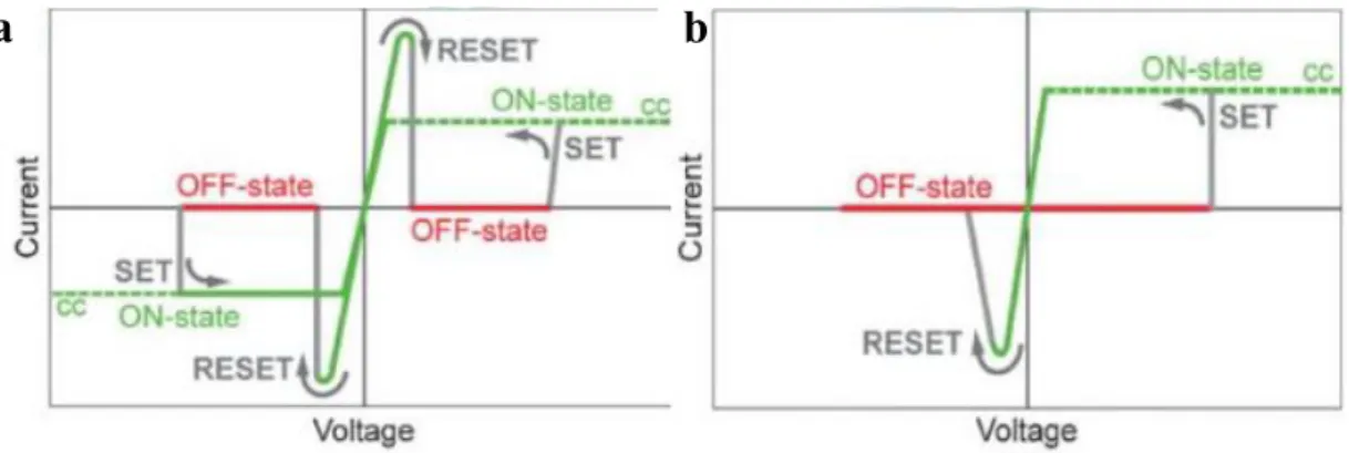
Resistance Switching Memory Devices based on Zinc Oxide Nanoparticles on Paper Substrates 3 Figure 1.2 - a) Typical I-V curve of a unipolar b) and bipolar resistive memory, (adapted from [20])
Analysing the publication in table 1, it is evident there is a novel area where it lacks a development of a ZnO RRAM using low cost techniques and low annealing temperatures, in order to make it possible to be fabricated in paper substrates. Thus this work aims to fill this gap. It will aim to create a ZnO RRAM on a paper substrate using low cost printing techniques as possible with lower temperature annealing than 150 °C. ZnO can be processed and printed, using solution precursors. In this work ZnO obtained from sol-gel method [33] and commercial nanoparticles (NPs) will be explored in ways to work as the active layer in RRAM devices
Table 1.1-Key parameters of the reported RRAM i.e. the substrate, the active layer, the position technique, te anealing temperature, the electrodes and the endurance
1.3
Screen Printing technique
Conventional techniques, such as chemical vapour deposition and sputtering, usually require vacuum and high-temperature conditions. Considering the fabrication environment and chemical compatibility, most of these fabrication processes are not suitable for paper-based device [28].Also, with increasing demands for more economic routes to manufacture electronic devices [34] and find fabrication methods that do not require high temperature process or annealing which is crucial when using paper substrates, various techniques for the fabrication of microelectronic devices, including screen printing, Nano-imprinting, ink jet printing, and direct printing, are generating an increasing interest.
In this work screen printing technique was chosen to fabricate 2 of the 3 layers which constitutes the device. However, the platinum bottom contact was deposited using E-beam evaporation, an expensive fabrication process compared to the low cost screen printing technique. Despite the possibility of printing platinum using Heraeus Silica and Metals, RP10001-145B ink, the required high annealing temperature impossibilities the use of paper substrates [35, 36]. The platinum is dispersed within an
YEAR SUBSTRATE ACTIVE LAYER DEPOSITION TECHNIQUE ANNEALING TEMPERATURE (°C)
ELECTRODES ENDURANCE
2016
[29] TiO2/SiO2/Si Co:ZnO Spin coating 550 Pt 50 cycles
2012
[30] Ti/SiO2/Si ZnO RF sputering RT Pt 10
6
2009 [7]
Stainless Steel
(SS) ZnO RF sputering RT
Au top
SS bottom 100
2016
[31] PEN ZnO:EVA
Thermal roll lamination
technique 150 ITO
WORM - write only
2014
[28] Paper TiO2 Screen printing 180
Ag top
C bottom 30 000 cycles
a
)
b
)
Resistance Switching Memory Devices based on Zinc Oxide Nanoparticles on Paper Substrates 4 organic resin which is completely burnt off during the firing process producing metal films of high purity. The temperatures required achieves 850 °C which is completely incompatible with paper [35, 36].
Screen printing, in which screen masks are used to deposit materials onto large-area substrates with high throughput, is considered as one of the scalable printing techniques and has been widely used in printed electronics. Benefiting from its simplicity, scalability and environment-friendly process, this technique shows tremendous potential for mass production of large-area electronics at very low cost [37]. In addition, screen printing allows patterning (to define which areas of the substrate receive deposition [38]).A basic concept of screen printing consists in applying pressure to the squeegee, it moves over the screen. When the squeegee enters in contact with the ink, it creates shearing stress to the ink and the viscosity is decreased. Then, the ink is transferred, in a controlled manner, through the apertures of a mesh and deposited on to a substrate. Any required pattern can be printed by blocking off appropriate mesh apertures with a photo emulsion layer to form a printing screen. The pattern definition is also dependent on the mesh count (number of threads per inch) [39]. An important parameter to control is the ink viscosity, that should be low enough for easy flow through the mesh under the shearing stress, but high enough to keep its form when deposited, and with the shearing stress removed, to prevent lateral flow. Viscosities, typically between 500 - 5000 cPs are referred to as desirable for this technique. Also, printing speed, angle and geometry of the squeegee, mesh size, material, strength and snap-off (distance between screen and substrate) are main factors to consider in order to achieve high-resolution patterning (30 - 50 µm), through this printing technique. In figure 1.3, is displayed a schematic draying of the used screen-printing present in CENIMAT|I3N.
Figure 1.3 - Schematic representation of the custom-made screen-printing present in CENIMAT|i3N[40]
1.4
Ink formulation for RRAM fabrication
Considering the importance of developing an ink that should have the ideal viscosity to achieve a high quality printing, this subsection will give an explanation of the selected materials for the ink development.
Resistance Switching Memory Devices based on Zinc Oxide Nanoparticles on Paper Substrates 7
2
M
ATERIALS
AND
METHODS
:
F
ABRICATION
,
OPTIMIZATION AND CHARACTERIZATION OF
Z
n
O
RRAM
DEVICES
The following chapter will present all the steps to develop, characterize and optimize the RRAM devices based on ZnO NPs. First it will be focused on the inks formulation that will be used as active layer. Next, it will be shown the architecture chosen for ZnO RRAM devices, explaining as well the several steps and techniques used for all of the layer depositions. At last, it will be listed all the characterization techniques selected to study the morphology and structure of the active layer, i.e. the ZnO nanoparticles dispersed into a cellulose matrix based on ethyl cellulose. Finally, the electrical characterization conducted for each device will be presented.
2.1
ZnO ink formulation materials and reagents
The methods adopted for preparing the active or semiconductor layer ZnO NPs screen printing paste, i.e. the ZnO nanoparticles dispersed into a cellulose matrix based on ethyl cellulose were based and adapted from the literature [43].
The binder solution was prepared by dissolving 5% wt EC 300 cP (C6H7O2(OC2H5)3; CAS:
9004-57-3) from Aldrich on an 80:20 toluene/ethanol solution (C6H5CH3; CAS: 108-88-3 / C2H6O;
CAS: 64-17-5). For its complete dissolution it should be 12 hours under stirring at 600 rpm.
Then, three different inks were synthetized, as depicted in table 2.1, in order to optimize the device and also to understand the role of ZnO, EC.
Table 2.1 - Inks composition developed in this work and its quantity
2.2
ZnO:EC RRAM by screen-printing
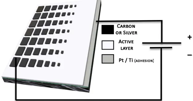
The architecture adopted in this work consists in the active layer sandwiched between two different contacts, as shown in the schematic representation, figure 2.1. In order to decrease the factors that could influence the RRAM behaviour, one of the electrodes must be inert and platinum was the chosen material. To keep the fabrication simple, a 100 nm thick platinum layer was deposited over 20 nm of titanium, to ensure the adhesion to the paper substrate. Both metals were deposited by E-Beam evaporation. The remaining layers were printed using a homemade screen-printing system described on figure 1.2
Before printing the active layer, the paper with platinum already deposited, should be subjected to an ultraviolet (UV) irradiation during 30 min through a UV-Ozone Cleaner – Novascan PSD-UV. After finishing the surface cleaning process, the semiconductor layer was printed through a mesh model 77-55 (mesh count 190, aperture 81 µm and thread diameter 55 µm), followed by 2 min annealing on a hotplate at 120 °C. Finally, some devices were also exposed for 15 min to UV irradiation.
ZnO
concentration (%) ZnO mass (g) Toluene/Ethanol + 5%EC mass (g)
A 0 0 10
B 10 1 9
Resistance Switching Memory Devices based on Zinc Oxide Nanoparticles on Paper Substrates 8 At last the top contact pattern (defined in figure 2.1) was printed using a mesh model 120-34 (mesh count 305, aperture 45 µm and thread diameter 34 µm), followed by 2 min annealing on a hotplate at 120 °C. For the top contact two different inks were tried: silver ink (PE-AG-530 ink, Flexible Silver Conductive Ink) and carbon ink (PE-C774, Carbon Resistive Ink), both from Conductive Compounds, Innovative Chemistry for High Tech Applications
Figure 2.1 Schematic representation of the architecture adopted in this work and their conections to the Agilent B1500A Semiconductor parameter analyzer
2.3
ZnO RRAM using printing pen
The architecture adopted is similar to the devices fabricated in subsection 2.2. This approach was used in order to get the active layer consisting only of ZnO nanoparticles, since the ink here used do not require high viscosity, hence the EC binder as used for screen-printing patterning. Here, the semiconductor layer was drawn using the Pen on Paper technique where we selected a parallel plate nib pen from Pilot and ZnO dispersion (50 wt. % in water) from Aldrich (CAS: 721077-100G) as the semiconductor layer. This semiconductor layer was dried at room temperature and in order to study the influence of its thickness and the number of printing steps were from one to three.
2.4
Characterization techniques
The active layers used in the devices were characterized by Scanning electron microscope (SEM) using the Hitachi TM 3030Plus Table Top Scanning electron microscope for cross section in order to determine the estimate thickness of the screen-printed layers.
Fourier transform Infrared (FTIR) spectroscopy was applied in order to evaluate the effect of UV irradiation on the semiconductor layer. The 40% ZnO ink was screen-printed on glass substrates, previously cleaned in acetone, IPA and DI water. The spectra were acquired between 4500-500 cm-1,
using a Nicolet 6700 FTIR Thermo Electron Corporation device.
Leica IC80 HD microscope and the LAS V4.3 software were used to measure the top contact dimensions.
The electrical characterization of the resistive memories was performed at room temperature using an Keysight B1500A semiconductor parameter analyser connected to a Cascade
Microtech EPS150 manual microprobe station, controlled by the software Keysight Easy Expert. As depicted in figure 2.1, the bottom electrode was connected to positive bias and the top electrode was grounded.
Resistance Switching Memory Devices based on Zinc Oxide Nanoparticles on Paper Substrates 9
3
RESULTS
AND
DISCUSSION
In this work, several devices were tested in order to study the influence of the active layer composition and thickness, as well the UV influence and the use of silver top electrode was studied for the 40%ZnO: EC. Table 3.1 resumes the fabricated devices characteristics and their nomenclature from here on out.
Table 3.1– All fabricated devices characteristics and their nomenclature
In this section it will be reported and discussed the electrical characterization of each modification introduced. The main objective in these study is to develop the suitable ink for resistive memory switching and the optimization of the fabrication methods i.e. active layer printing steps, the use or not of UV irradiation after the deposition of the active layer and the electrodes material. At the end, it will attempt to find a suitable mechanism for the memory effect on these devices.
3.1
Study of memory effect when using only ZnO NPs as active layer
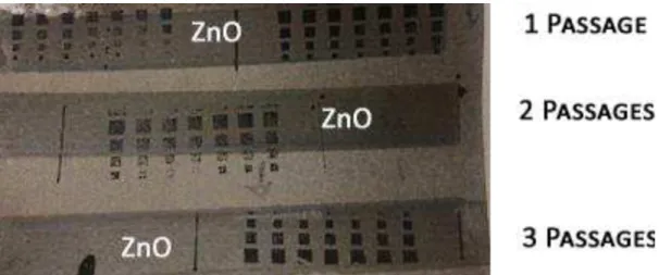
Using screen-printing technique is almost impossible to print ZnO without binder, so it was chosen drawing pen technique to draw lines consisting only of ZnO with the intention to comprehend the importance of ZnO itself and also if EC is having an important role to the memory effect. The architecture adopted consists in bottom platinum contact and screen-printed carbon top electrode. Figure 3.1, shows the surface of
Name Composition Printing technique
Printing steps
UV
irradiation Top Electrode
Bottom
electrode Substrate
EC Only EC (A) printing Screen- 2
Screen-printed Carbon
Screen-printed Carbon
Paper
ZnO1
Only ZnO Drawing Pen 1
E-beam Platinum
ZnO3 3
10ZnO 10%ZnO+EC (B)
Screen-printing 2
40ZnO1
40%ZnO+EC
(C) printing
Screen-1
40ZnO2C
2
40ZnO2Ag Screen-printed
Silver
40ZnO3
3 Screen printed Carbon
40ZnO3no
Resistance Switching Memory Devices based on Zinc Oxide Nanoparticles on Paper Substrates 10 Figure 3.1 - Image of the surface of drawn ZnO lines with different number of passages between screen-printed
carbon top contacts and E-beam platinum bottom contact on paper substrates
Figure 3.2 resumes the electrical characterization of these devices without compliance (delimited by equipment limitation) and using 200 ms of delay time, 100 mV of step size. For one writing pen passage (ZnO1), it is evident the hysteresis is low and despite of having some memory effect, it only achieved one cycle, where the first run in green, the device switched from LRS to HRS (RESET) at -20 V and at the second run in blue, the device switched from HRS to LRS (SET) at 25.2 V. The difference between LRS and HRS around half order of magnitude which is too low to distinguish the two resistance states. Also the device remained stable after 100 s reading at 500 mV. As well, the resistance of the device is 21 kΩ.
Figure 3.2 b) shows the electrical characterization of one device, when the number of pen passages is increased to three (ZnO3). It was made two I-V sweeps: the first one from -5 V o 5 V in blue and the second from -10 V to 10 V in magenta. In both curves, the hysteresis is completely disappeared, acting a resistor. Moreover, the resistance increased one order of magnitude to 241 kΩ due to increase of ZnO thickness.
With this experiment, using only ZnO in the active layer, it had low hysteresis. Thus, the presence ethyl cellulose seems to plays a crucial role to the memory effect.
Figure 3.2 - I-V curves of ZnO between carbon top contact and platinum bottom contact on paper substrate for: a) one writing step b) three writing steps
Resistance Switching Memory Devices based on Zinc Oxide Nanoparticles on Paper Substrates 11
3.2
Study the memory effect of EC as active layer
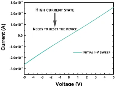
Figure 3.3 shows the initial I-V sweep from -5 to 5 V on a fully-printed structure using only EC as active layer (2 printing steps of screen-printed EC between screen-printed carbon electrodes), showing that the device is in a high current state due to its high current reaching 1 mA at 2 V. So the next step consists in performing a RESET.
Figure 3.3 - First IV sweep realized during electrical characterization, showing a device in LRS
Figure 3.4 resume the I-V sweeps made as well the reading tests at 500 mV for 10s. The steps 1 to 3 correspond to a successful attempt to RESET the device, where a voltage sweep was made from 0 to -40 V, with a delay time of 500 ms, a step size of 100 mV and a current compliance of 0.1 A. Using this structure, the first RESET switch occurred at very high voltage, at -27.2 V with a current of 35.7 mA. However, at -2 V the current raised and it came to an intermediate current state.
The steps 4 to 6 correspond to a SET switch. Nevertheless, at 2.2 V the current drop to an intermediary current state to a lower current state and at 9.8 V the device was SET, reaching the compliance of 100 µA. Then the device was erased (step 7) and the voltage value dropped to -2 V when compared to the 1st cycle. However, the device never returned to LRS, achieving only one cycle. One
reason to the poor performance could be related to the ink viscosity. As the ink does not contain ZnO, which it adds viscosity to the ink itself, the viscosity is too low to ensure a good deposition.
Due to low endurances cycles is not considered as a reliable memory. Thus it could be for two reasons: the formation a carbon filament due to redox reaction on the electrodes (electrochemical memory) in the presence of ethyl cellulose. The literature does not support the conductive bridge memory effect since carbon is inert [28]. Also using conductive carbon (it was used a conductive carbon ink) the current density needed for form a filament is 350 MA/cm2 [44]. Since the area of the smallest
electrodes used is 2.5 x 10⁻³ cm2 and the maximum current of the characterization equipment is 0.1 A,
the theoretical maximum current density that could achieve is 40A/cm2, five orders of magnitude below
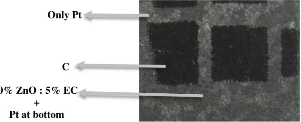
Resistance Switching Memory Devices based on Zinc Oxide Nanoparticles on Paper Substrates 12 Only Pt
C
10% ZnO : 5% EC +
Pt at bottom
Figure 3.4 - a) Endurance cycles performed of EC between carbon top and bottom contact on paper substrate b) Rreading tests for 100 s at 500 mV after the SET and RESET the device
3.3
Study the memory effect when using 10% ZnO with 5 % EC as active layer
RRAM on paper substrates were fabricated using an ink that contains 10 % wt ZnO with 5% wt EC, between an E-beam deposited platinum and screen-printed carbon or silver electrodes. As depicted in figure 3.5, making a visual inspection of the substrate fabricated, it is visible the lack of uniformity of the active layer, even after two printing steps. Looking only for the platinum and the active layer, the darker zones of the device correspond the screen-printed active layer while the lighter areas, especially in top left of the device, suggest the active layer is not present. The cause of poor printing process could be attributed to the clogging of the mesh causing the lack of uniformity. However, a visual inspection to the mesh used to print the active layer didn’t show any signs of obstruction. The other reason that could be caused the poorly printed active layer is related with the low viscosity of the 10 % wt ZnO ink that do not allow for good film formation.
Figure 3.5 - Image of the surface with screen-printed 10% ZnO : 5% EC layer with carbon top contacts on paper substrates
Electrical characterization was performed on this substrate. The positive bias was connected to the platinum electrode and the carbon contact was grounded. Figure 3.6 shows the initial I-V curve from 0 to 3 V. In this range of voltage, the current is lower than 100 nA, meaning the device is virgin and it needs an electroforming process.
a)
Resistance Switching Memory Devices based on Zinc Oxide Nanoparticles on Paper Substrates 13 .
Figure 3.6 - First I-V sweep realized during electrical characterization, showing a virgin device
The next step consists to perform an electroforming process. Figure 3.7 a) shows I-V curves for the electroforming process in magenta and its erase in blue. The steps 1 to 6 represents the electroforming process which it consists to switch from high resistance state (low current) to a lower resistance state (higher current). At 5.6 V the device changed from HRS, where the current is below 10 nA, to LRS, reaching current values around 1 mA. Next, as shown in figure 3.7 b), it was made a reading test for 100 s at 500 mV to ensure the device was at LRS. At 500 mV, the current is 19 µA and it remained stable over 100 s. Subsequently, it was performed the RESET switch, or erase process. The steps 7 to 11 represents the RESET switch, that occurred at -10.3 V and reaching a current of 1.3 mA. Making a reading after RESET the device, the current dropped to values below 1 nA. Thus, the difference between the two states is at least four orders of magnitude.
Figure 3.7 -a) First cycle performed on 10 % Zno : 5 % EC with carbon top contact and platinum bottom contact (10ZnO) b) Read test for 100 s at 500 mV after the first SET and RESET the device in a)
Figure 3.8 shows the 2nd cycle, initially making I-V sweep to positive voltages in order to SET
the device. However, even make I-V sweeps in both sides, the current value remains low, below 1 µA, which it means the change did not occur and it remains at HRS. The noise associated could indicate a competition between formation and rupture of the conductive filaments by the current itself.
Resistance Switching Memory Devices based on Zinc Oxide Nanoparticles on Paper Substrates 14 Figure 3.8 - Second cycle performed on 10 % Zno : 5 % EC with carbon top contact and platinum bottom
contact (10ZnO)
Thus, using the ink that contains 10 % ZnO, it only managed one cycle. The percentage of ZnO could not be enough and the higher EC/ZnO ratio could lead to instability. Nevertheless, it is crucial to perform more tests to confirm the hypothesis. Also as seen in figure 3.5 the printing quality were poor due to the low viscosity of the ink and as result several devices were short circuited.
3.4
Study the memory effect when using 40% ZnO with 5 % EC as active layer
As discussed in subsection 3.3, the biggest problem concerning the endurance of the memories when using a ZnO concentration of 10 % could be related to the low viscosity in the ink and some instability caused by the high EC/ZnO ratio. Therefore, one solution consists in increasing the concentration of ZnO, which it increases also the ink viscosity. Consequently, it was made several devices using 40% ZnO: 5%EC ink, where several factors were changed in order to optimize the device as depicted in table 3.2: the number of printing steps, the UV irradiation after screen-printing the active layer and the use of silver top electrode instead of carbon.
Table 3.2 - Device characteristics using 40% ZnO ink
Name Active layer Composition Printing technique Printing steps UV
irradiation Top Electrode
Bottom
electrode Substrate
40ZnO1
40%ZnO+EC
(c) printing
Screen-1 Screen-printed
Carbon 40ZnO2
C 2
E-beam
Platinum Paper 40ZnO2
Ag
Screen-printed Silver
Resistance Switching Memory Devices based on Zinc Oxide Nanoparticles on Paper Substrates 15 3.4.1 UV irradiation influence on the active layer
The study of the influence of the UV irradiation after deposition of the ZnO:EC layer was realised by ATR-FTIR. The 40 % ZnO : 5 % EC ink was screen-printed on glass substrates and annealed at 120 °C. The difference consists in one sample was UV irradiated for 15 minutes and the other sample was not irradiated.
In figure 3.9 shows the ATR-FTIR spectrum for the ink with these two distinct treatments performed. For EC, the peak at 3500 cm-1 represents the stretching of O-H groups both in the closed
ring structure and in intra/intermolecular hydrogen bonds. The peaks around 2980-2870 cm-1 may
indicate CH stretching and the distinct peak at 1375 cm-1 refers to CH
3 bending. As well, the small peak
at 1440 cm-1 represents CH
2 bending, and the broad peak around 1100 cm-1 might be due to C-O-C
stretching in the cyclic ether [45]. In both samples it is evident the presence of the EC, which it means the EC do not degrade when exposed to 15 min of UV irradiation. Additionally, the decrease of intensity at 3500 cm-1 and at 1100 cm-1, when submitted UV irradiation could be related the loss of toluene and
ethanol that did not fully evaporate during annealing.
Figure 3.9 - ATR-FTIR spectra of the ZnO NPs:EC ink after being screen-printed on a glass substrate and submitted or not UV irradiation for 15 min.
Figure 3.10 shows the electrical characterization of the best device not submitted to UV irradiation. Electroforming process was necessary to preform since the device was virgin (an example is shown in fig 3.6). The device switches from HRS to LRS at 14.5 V. The RESET voltage increased over the cycle: from -3.9 V at 1st cycle to -10 V at 5th cycle. The SET occurred from 4.8 to 14.9 V, which
is higher than the electroforming process occurred. Thus it is a sign of non-conventional bipolar behaviour.
Resistance Switching Memory Devices based on Zinc Oxide Nanoparticles on Paper Substrates 16 Figure 3.10 - Endurance cycles performed on 40 % Zno : 5 % EC with carbon top contact and platinum bottom
contact on paper substrate without UV irradiation
Most important, in figure 3.11 b) was performed a retention test, for 1500 s at 500 mV. At 1450 s the current in LRS started to drop two orders of magnitude, from 10.5 µA to 100 nA, showing a sign of instability. Thus, it might conclude that making an UV irradiation after printing the active layer the memory become more stable. UV irradiation facilitates photodecomposition or photoreaction of ZnO into Zn2+ [46] creating more oxygen vacancies. As consequence, the devices that were submitted UV
irradiation achieved better performance due to the elimination of solvents in the substrate that could cause electrical failure and the creation of Zn2+ radicals that induce more carries.
Figure 3.11 - a) average level of resistence at HSR and LSR after the SET and RESET the device in 3.10, comparing to a device that was made UV irradiation after printing the active layer b) Reading retention for 1
500 s at 500 mV after SET and RESET the device
Resistance Switching Memory Devices based on Zinc Oxide Nanoparticles on Paper Substrates 17
3.5
Study the influence of active layer (ZnO:EC) thickness
The manual screen printing stage used in this work does not allow for a very accurate process. as seen by visual inspection of the fabricated devices in figures 3.14 and 3.19. So, it was crucial to check the layer uniformity in order to estimate the thickness, especially the ZnO mixed with EC layer which is crucial to the memory effect. One method to estimate the layer thickness is profilometry. However, this is not an adequate method due to the reasons listed: profilometry can only be used in smooth substrates and paper has high surface roughness. Also the active layer is delicate. Even using low force, when the tip makes pressure to the surface, it damages the layer. Using a glass substrate could be a solution to the first issue, but its more relevant to understand the deposition uniformity on paper substrate due to the high roughness. So making cross section of the devices produced and analysing using a SEM equipment would be important to understand the deposition uniformity and as important, to relate the thickness of ZnO with EC layer with the device performance.
The cross sections were made after performing electrical characterization, using liquid nitrogen in order to brake the cellulose fibres, avoiding smashing them, unlike the cuts made using scissors and razors. Four cross sections were performed in different substrates where the only difference was the number of ZnO + EC passages from a single printing step to three printing steps. All the SEM images have a magnification of 800 x and were edited using software Photoshop cc 2015 by Adobe.
a)
b)
c)
d)
Figure 3.12 - SEM images of device cross sections with 800x of magnification and the ZnO:EC thickness over the distance graphic: a) with 1 printing step b) with 2 printing steps c) with 3 printing steps d) with 3
Resistance Switching Memory Devices based on Zinc Oxide Nanoparticles on Paper Substrates 18 On SEM images in figure 3.12 all the layers are visible even the 100 nm thick platinum. Each layer was colorized using blue tones, which it can be used to easily distinguish them. The graphics of each image shows the carbon and ZnO plus EC thickness across the image when twenty measurements were made on each layer. It is evident that the ZnO with EC layer is not uniform over the image. This conclusion is expected because even perform a visual analysis at naked eye to the substrates the change of opacity is a strong evidence of non-uniformity of the layer. Also the average thickness of carbon in all conditions is 8.00 µm with a standard derivation of 2.20 µm which is perfectible acceptable for a screen-printed process. On the other hand, for ZnO mixed with EC layer the layer thickness rises with the increase of the number of printing steps: from one printing step the thickness is 9.37 µm with a standard derivation of 2.07 µm, for two printing steps the average thickness is 26.34 µm with a standard derivation of 3.40 µm. For three printing steps it was measured in two different locations on the substrate: one has an average thickness of 22.29 µm with a standard derivation of 2.12 µm (figure 3.12 c)) and another have average thickness of 30.37 µm with a standard derivation of 4.64 µm (figure 3.12 d)). Discussing this data leads the ZnO + EC layer is not uniform, varying form 22.29 µm to 30.37 µm, an increasing of 36 %. Another inconsistency is the ZnO + EC layer thickness for two printing steps is higher than having three printing steps. This could be justified for 3 printing steps the ink didn’t pass through the mess creating a non-uniform deposition. Also for two printing steps, the zone where the cross section was made, it could have deposited a big amount of ink, creating a thicker layer. Thus it reveals the biggest issue of the manual screen-printing process: lack of uniformity over the film. This problem is related with the inconstant application of force through the squeegee or printing speed applied by the operator.
3.5.1 Comparison of electrical performance for different active layer thickness
Figure 3.13 - a) 2nd cycle of 40ZnO1C, 40ZnO2C and 40ZnO3C; b) HRS current over the cycles for two printing steps and three printing steps of ZnO:EC layer
In figure 3.13 relates the performance of each device for different printing steps. In figure 3.20 a) is depicted the I-V curves made on 2nd cycle for two and three printing steps and as well a typical
behaviour when has one printing step. The 40ZnO2C and 40ZnO3C have similar behaviour, but using three printing steps the hysteresis is higher. In figure 3.13 b) is evident the higher memory window at least one order of magnitude compared to two printing steps. This could be explained to increasing of thickness more isolate the layer become in HRS, meaning lower current in this state. However, there is a drawback. The voltage needed to set the device is bigger or the delay time should be increased.
For one printing step the behaviour is different. It shows hysteresis but there is not any abrupt change of current. In the positive voltage the current level when made the forward sweep (0 V to 40 V) is lower than backward sweep (40 V to 0). At negative voltages it is the opposite: the current level when
Resistance Switching Memory Devices based on Zinc Oxide Nanoparticles on Paper Substrates 19 made the forward sweep (0 V to -40 V) is higher than backward sweep (-40 V to 0). Further investigation should be carried in order to understand this behaviour.
3.5.2 Two printing steps of 40% ZnO:5% EC with silver top contact (40ZnO2Ag)
As shown in figure 3.14, after two printing steps (40ZnO2C), the homogeneity of the active layer is acceptable. As well, the thickness in the right side of the substrate is lower, due to the decrease of opacity. Thus with two passages the 40% ZnO : 5% EC layer has an opaque white colour due to the higher amount of ZnO present in this synthetized ink.
Figure 3.14 - Image of the surface with screen-printed 40% ZnO : 5% EC layer and also silver and carbon top contacts on paper substrates
Figure 3.15 shows the electrical tests performed in the best performance device in this substrate. All I-V sweeps used a delay time of 200 ms, a current compliance of 0.1 mA for the write process, a voltage step of 100 mV.
Analysing the cycles endurance (figure 3.15 a)), it was achieved seventeen full cycles, considering that the device did not write successfully on 18th cycle. In colour, is represented some cycles
(2,3, 10 and the last) where the device was programed in bipolar: the SET occurs at positive voltages the RESET occurs at negative voltage.
As depicted in figure 3.15 b), the switching probability of the SET and RESET over the voltage is calculated using the data obtained by the I-V sweeps made. The device transited from HRS to LRS (SET) happened in the interval of voltage from 2.5 V to 6.8 V and transited from LRS to HRS (RESET) occurred in the interval of voltage from -2 V to -9 V. As important, the voltage that occurred the resistive switches does not follow any tendency (increasing or decreasing) over the cycles. Annex A contains the switching values for each cycle.
Figure 3.15 c) depicts the resistance value of LRS and HRS after SET and RESET the device respectively. This test is important to verify if the change of resistance were successful. Moreover, with exception of 5th and 18thcycle, the average LRS value is 24 kΩ ± 5 kΩ and the average HRS value is 5
MΩ ± 10 MΩ. In opposite to the constant values of LRS, the values of HRS vary from 123 kΩ at 7th
cycle to 35.9 MΩ at 2nd cycle. Also important with exception of 5th and 18th cycles, the difference
between HRS and LRS is at least one order of magnitude which is enough to distinct the two states. However, at 5th and 18th cycles, the resistance value in LRS is inferior to the highest HRS value, which
Resistance Switching Memory Devices based on Zinc Oxide Nanoparticles on Paper Substrates 20 Figure 3.15 - a) Endurance cycles performed on 40 % Zno : 5 % EC with carbon top contact and platinum bottom contact on paper substrate b) Switching probability over voltage c)average LRS and HSR current after the SET and RESET the device in a) for 18 cycles
.
Figure 3.16 - Retention test for 2500 s at 500 mV
a)
Resistance Switching Memory Devices based on Zinc Oxide Nanoparticles on Paper Substrates 21 At the 15th cycle, it was performed a retention test for 2500 s at 500 mV. Figure 3.16 shows the
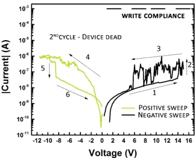
retention results at LRS and HRS after SET and RESET the device respectively. The device maintained very stable in both states, with a current of 19.4 µA at the low resistivity state (LRS) and 0.38 µA at the high resistivity state (HRS). The current ratio between the two states is around 50, which is sufficient to distinguish the two resistivity states. Nonetheless, as seen in figure 3.17, the device has lost the capacity to have two distant states at reading voltage (after hit the compliance it went abruptly to the HRS) leading to failure.
Figure 3.17 - SET process in 17th and 18th cycle, evidencing the device failure 3.5.3 Two printing steps of 40% ZnO:5% EC with silver top contact (40ZnO2Ag)
Compared to the previous substrate, the only change was the use of silver contacts instead of carbon contacts. In this case the positive bias was connected to the platinum and the silver contact was grounded. In figure 3.18, resuming the endurance tests performed, all I-V sweeps performed used a delay time of 200 ms, a current compliance of 1 mA for the SET process, a voltage step of 100 mV. In this case the first IV sweep made was from 0 to 7 V, indicating that the device was in LRS. Therefore, it was executed a positive sweep with the purpose to reset the device. At 16 V the current started to drop from 200 mA to 10 µA. However, when the voltage was decreasing to zero, the device became unstable where the current increase and decrease abruptly. That occurrence happened in all RESET process. On the other side, the set process was more stable, where the SET voltage increased from -4.4 V at 1st cycle
to -12.8 at 3rd cycle.
Making the reading test at 500 mV for 100s shows the resistance in HRS varies from 14 MΩ at 2ndcycle to 110 MΩ at 3rd cycle and the LRS varies from 69 kΩ at 1stcycle to 875 kΩ at 3rd cycle. Thus
the minimum RHRS/RLRS ratio is 16 at the 2nd cycle, which is similar compared to the carbon top electrode
devices. Nevertheless, the performance achieved using screen-printed silver top contacts were worse compared using carbon contacts. The SET and RESET take place at higher voltage and it only achieved three cycles instead twenty cycles achieved when using carbon contacts.
![Figure 1.1 a) Application of a zinc oxide nanorods in textile substrate targeting the development of a diode [6]](https://thumb-eu.123doks.com/thumbv2/123dok_br/16698375.743908/21.892.127.767.263.535/figure-application-oxide-nanorods-textile-substrate-targeting-development.webp)
![Figure 1.3 - Schematic representation of the custom-made screen-printing present in CENIMAT|i3N[40]](https://thumb-eu.123doks.com/thumbv2/123dok_br/16698375.743908/24.892.124.753.509.839/figure-schematic-representation-custom-screen-printing-present-cenimat.webp)