1006 Brazilian Journal of Physics, vol. 35, no. 4A, December, 2005
Synthesis and Characteristics of SnO
2
Nanorods on Pd-Coated Substrates
Hyoun Woo Kim, Seung Hyun Shim, and Ju Hyun Myung
School of Materials Science and Engineering, Inha University, Incheon 402-751, Republic of Korea
Received on 2 August, 2005
We have fabricated tin oxide (SnO2) nanorods on palladium-coated substrates by carrying out the thermal
evaporation of solid Sn powders. We have employed X-ray diffraction, scanning electron microscope, transmis-sion electron microscope and photoluminescence (PL) spectroscopy to characterize the synthesized products. The obtained 1D nanomaterials with a jagged surface were SnO2 with rutile structure. PL spectra exhibited
visible light emission.
I. INTRODUCTION
Tin oxide (SnO2) is an important metal oxide. As a
trans-parent conducting oxide, it has a long history of use as an electronic conductor, primarily in the form of thin films. In addition, the material has received a great deal of attention due to its applications in optoelectronic devices including flat panel displays and solar energy cells [1].
Inorganic materials with different morphologies and size can exhibit different properties [2], even if they are made up of the same elements. Accordingly, various structural and mor-phological forms of SnO2materials have been fabricated over
the past several years, including nanowires [3,4], nanorib-bons or nanobelts [5-8], nanorods [9], nanotubes [10], nan-odiskettes [11], and nanocomposites [12,13].
Although carbon nanotubes have been synthesized using the palladium (Pd) catalyst [14-16], to our knowledge, syn-thesis of any inorganic nanomaterial including SnO2, on the
Pd substrate has not been reported to date. Furthermore, Pd is a platinum-group metal with good corrosion resistance and has been studied as the VLSI materials [17]. In this paper, we report a thermal evaporation approach, by which we have produced the SnO2nanorods on Pd-coated Si substrates. We
have investigated the samples with respect to their structural and photoluminescence (PL) characteristics.
II. EXPERIMENTAL
Pure Sn powders were placed in an alumina boat, which was put in the middle of quartz tube inserted in a horizon-tal tube furnace. We used Si(001) as a starting material onto which a layer of Pd was deposited. On top of the boat, a piece of the substrate was placed with the Pd-coated side down-wards. The vertical distance between the alumina boat and the substrate was approximately 10 mm. After evacuating the quartz tube to∼10−3Torr, the furnace was heated to 900oC
from room temperature with no gas flow. During the exper-iment, the furnace was kept at temperature and pressure, re-spectively, of 900oC and 150 mTorr in an air flow for 2 h. After evaporation, the substrate was cooled down and then re-moved from the furnace for analysis. A white layer was found on the surface of the substrate.
Glancing angle X-ray diffraction (XRD: CuKα1radiation) patterns were obtained on a Philips X’pert MRD
diffractome-ter with an incidence angle of 0.50. Scanning electron
mi-croscopy (SEM) studies were carried out on a Hitachi S-4200. Further structural analysis using transmission electron microscopy (TEM) was performed on a Philips CM-200. For TEM observation, the products were ultrasonically dispersed in acetone, and then a drop of the suspension was placed on amorphous carbon films supported by copper grids and dried in air. PL spectrum was measured at room temperature by a 325 nm He-Cd laser (Kimon, 1K, Japan).
III. RESULTS AND DISCUSSION
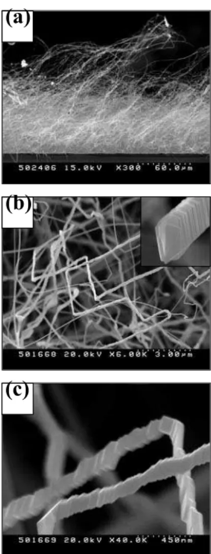
Figure 1a shows the typical side-view SEM image of the product, indicating that this wool-like material consists of ag-gregates of one-dimensional (1D) nanostructures. The SEM image reveals that the growth direction of the nanostructure is randomized. Fig. 1b shows the SEM image of the prod-ucts with a closer view, revealing that the product comprises the straight, bent, and crooked rod-like structures. Statistical analysis of many SEM images shows that average diameter of these nanostructures varies from 30 to 300 nm and length reaches up to several tens of micrometers. The upper right in-set in Fig. 1b reveals that no catalyst particle can be seen at tips of the 1D structures. Fig. 1c shows the high magnification SEM image enlarging an area of Fig. 1b. The jagged-edged or saw-like structure is apparent. Although similar structure has been observed in the case of MgO [18], to the best of our knowledge, no similar SnO2structure was reported in the
lit-erature previously.
Figure 2 shows a typical XRD pattern recorded from the products. The Miller indices are indicated on each diffraction peak. The diffraction peaks of the (110), (101), (200), (211), (220), (002), (310), (112), (301), (202), and (321) planes can be readily indexed to the tetragonal rutile structure of SnO2
with lattice constants of a=4.738 ˚A and c=3.187 ˚A (JCPDS File No. 41-1445). No obvious reflection peaks from the impuri-ties, such as unreacted Sn or other tin oxides, were detected, indicating the high purity of the products. In the XRD mea-surements, the angle of the incident beam to the substrate sur-face was approximately 0.50, and the detector was rotated to scan the samples. Therefore, we surmise that the peaks are mainly from the products.
magnifica-Hyoun Woo Kim et. al. 1007
FIG. 1: (a) Low magnification side-view and (b) closer-view SEM images of the products. Inset shows the end of a nanostructure. (c) High magnification SEM image.
tion TEM image is shown in Fig. 3a, indicating that the bent nanorod has the jagged surface, agreeing with SEM images. The associated selected area electron diffraction (SAED) pat-tern (Fig. 3b) taken from the nanorod can be indexed as a tetragonal rutile SnO2single crystal, in good agreement with
the XRD results presented above. Representative high res-olution TEM (HRTEM) image is given in Fig. 3c. Lattice fringes are clearly visible from the image, revealing its single crystalline nature. The interplanar spacings are approximately 0.237 nm and 0.176 nm, respectively, corresponding to the (020) and (211) planes of tetragonal rutile SnO2.
In the present work, although the Pd-coated substrate was employed, there was no evidence of Pd-containing particles at tips of the structures. Therefore, the growth of the SnO2
structure in the present route cannot be dominated by a vapor-liquid-solid (VLS) mechanism. This type of growth, which is close to vapor-solid (VS) process, might be attributed to the diffusion-limited process in an oxygsupersaturated en-vironment [19]. When the synthesis was carried out in the highly oxygen-abundant environment; i.e. under a relatively
FIG. 2: XRD pattern of the products.
higher oxygen pressure of 1000 mTorr (compared to the air pressure of 150 mTorr in the present study), we obtained the cluster-like structures without any thin nanorod. The varia-tion of SnO2structural morphology with O2content indicates
that O2gas plays an important role in controlling nucleation
and growth of SnO2nanorods. It is generally agreed that the
SnO(g), which forms at the initial stage of oxidation of Sn (Sn(s) + 1/2O2(g) →SnO(g)), is metastable and decompose
according to the reaction [20]: 2SnO(g)→SnO2(s) + Sn(l).
The additional oxygen may facilitate large supersaturation of O2gas and thus SnO gas in the gaseous state, resulting in fast
condensation. Under low supersaturation, narrow 1D struc-tures are easy to grow. Under high supersaturation, however, it may activate the secondary growth sites and heterogeneous nucleation on the side of the 1D structures, tending to produce the thicker structures. In the present synthesis route, while elevating the temperature with no gas flowing, we surmise that Pd layer stays pure or preferentially transforms to stable Pd silicide compounds. Therefore, it may provide negligible amount of additional oxygen to the growing SnO2
nanostruc-tures at the synthesis temperature of 900oC, keeping the thin 1D nanostructures from being thicker. Our experiments un-der the same condition using other substrate materials which comprise oxygen, resulted in the generation of the cluster-like or thick structures, agreeing with the above speculation. Ef-forts are now in progress to pursue these routes in more detail to reveal the synthesis mechanism.
Room-temperature PL spectra of the as-synthesized prod-ucts were measured and shown in Fig. 4. Visible emissions with a peak wavelength position of around 591 nm (corre-sponding to 2.10 eV) is dominantly observed. The visible light emission is known to be related to defect levels within the band gap of SnO2, associated with O vacancies or Sn
interstitials that have formed during the synthesis process [21-23]. A similar emission has been reported in the case of SnO2nanoribbons synthesized by laser ablation [21] and
1008 Brazilian Journal of Physics, vol. 35, no. 4A, December, 2005
FIG. 3: (a) TEM images of a SnO2nanorod. (b) Associated SAED
pattern of the [102] zone axis. (c) HRTEM image.
IV. CONCLUSIONS
In summary, we have demonstrated the production of SnO2
nanorods on Pd-coated substrate by heating Sn powders at 900oC. SEM image and TEM analysis coincidentally indicate that the product consists of nanorods with a jagged surface. The results of XRD, TEM and SAED pattern indicate that the SnO2nanorods have a tetragonal rutile-type crystalline
struc-ture. We speculate about the growth mechanism and need deep study in the future. The PL measurement shows an ap-parent visible light emission band centered at around 591 nm. Compared with SnO2nanostructures reported previously, the
SnO2nanorods in the present study exhibit different structural
characteristics, which may lead to novel applications in minia-turized devices.
FIG. 4: Room temperature PL spectrum with an excitation wave-length at 325 nm.
Acknowledgement
This work was supported by INHA UNIVERSITY Re-search Grant.
[1] N. Amin, T. Isaka, A. Yamada, and M. Konagai, Sol. Energy Mater. Sol. Cells67, 195 (2001).
[2] J. Hulliger, Angew. Chem., Int. Ed. Engl.33, 143 (1994). [3] A. Kolmakov, Y. Zhang, G. Cheng, and M. Moskovits, Adv.
Mater.15, 997 (2003).
[4] J. K. Jian, X. L. Chen, T. Xu, Y. P. Xu, L. Dai, and M. He, Appl. Phys. A75, 695 (2002).
[5] Z. L. Wang and Z. Pan, Adv. Mater.14, 1029 (2002).
[6] J. Q. Hu, X. L. Ma, N. G. Shang, Z. Y. Xie, N. B. Wong, C. S. Lee, and S. T. Lee, J. Phys. Chem. B106, 3823 (2002). [7] X. L. Ma, Y. Li, and Y. L. Zhu, Chem. Phys. Lett.376, 794
(2003).
[8] S.H. Sun, G. W. Meng, Y. W. Wang, T. Gao, M. G. Zhang, Y. T. Tian, X. S. Peng, and L. D. Zhang, Appl. Phys. A76, 287 (2003).
[9] D.-F. Zhang, L.-D. Sun, J.-L. Yin, and C.-H. Yan, Adv. Mater.
15, 1022 (2003).
[10] Z. R. Dai, J. L. Gole, J. D. Stout, and Z. L. Wang, J. Phys. Chem. B106, 1274 (2002).
[11] Z. R. Dai, Z. W. Pan, and Z. L. Wang, J. Am. Chem. Soc.124, 8673 (2002).
[12] J. Nemeth, I. Dekany, K. S¨uvegh, T. Marek, Z. Klencsar, A. Vertes, and J. H. Fendler, Langmuir19, 3762 (2003).
Hyoun Woo Kim et. al. 1009
[14] C. J. Lee, J. Park, J. M. Kim, Y. Huh, J. Y. Lee, and K. S. No, Chem. Phys. Lett.327, 277 (2000).
[15] R. Vajtai, K. Kordas, B. Q. Wei, J. Bekesi, S. Lepp¨avuori, T. F. George, and P. M. Ajayan, Mater. Sci. Eng. C19, 271 (2002). [16] Y. M. Wong, S. Wei, J. L. Davidson, W. Hofmeister, J. H.
Huang, and Y. Cui, Diamond Relat. Mater.13, 2105 (2004). [17] D. Dwivedi, R. Dwivedi, and S. K. Srivastava, Sens. Actustors
B71, 161 (2000).
[18] K. P. Kalyanikutty, F. L. Deepak, C. Edem, A. Govindaraj, and C. N. R. Rao, Mater. Res. Bull.40, 831 (2005).
[19] J. Guojian, Z. Hanrui, Z. Jiang, R. Meiling, L. Wenlan, W. Fengying, and Z. Baolin, J. Mater. Sci.35, 63 (2000).
[20] D.-W. Yuan, R.-F. Yan, and G. Simkovich, J. Mater. Sci.34, 2911 (1999).
[21] J. Hu, Y. Bando, Q. Liu, and D. Goldberg, Adv. Func. Mater.
13, 493 (2003).
[22] B. Cheng, J. M. Russell, W. Shi, L. Zhang, and E. T. Samulski, J. Am. Chem. Soc.126, 5972 (2004).
![FIG. 3: (a) TEM images of a SnO 2 nanorod. (b) Associated SAED pattern of the [102] zone axis](https://thumb-eu.123doks.com/thumbv2/123dok_br/18981154.457071/3.892.160.358.84.696/fig-tem-images-sno-nanorod-associated-saed-pattern.webp)
