SWITCHMODE
Pulse Width
Modulation Control Circuit
The TL494 is a fixed frequency, pulse width modulation control
circuit designed primarily for SWITCHMODE power supply control.
Features
•
Complete Pulse Width Modulation Control Circuitry
•
On−Chip Oscillator with Master or Slave Operation
•
On−Chip Error Amplifiers
•
On−Chip 5.0 V Reference
•
Adjustable Deadtime Control
•
Uncommitted Output Transistors Rated to 500 mA Source or Sink
•
Output Control for Push−Pull or Single−Ended Operation
•
Undervoltage Lockout
•
NCV Prefix for Automotive and Other Applications Requiring Site
and Control Changes
•
Pb−Free Packages are Available*
MAXIMUM RATINGS (Full operating ambient temperature range applies, unless otherwise noted.)
Rating Symbol Value Unit
Power Supply Voltage VCC 42 V
Collector Output Voltage VC1,
VC2
42 V
Collector Output Current (Each transistor) (Note 1)
IC1, IC2 500 mA
Amplifier Input Voltage Range VIR −0.3 to +42 V
Power Dissipation @ TA≤ 45°C PD 1000 mW
Thermal Resistance, Junction−to−Ambient RqJA 80 °C/W
Operating Junction Temperature TJ 125 °C
Storage Temperature Range Tstg −55 to +125 °C
Operating Ambient Temperature Range TL494B
TL494C TL494I NCV494B
TA
−40 to +125 0 to +70 − 40 to +85 −40 to +125
°C
Derating Ambient Temperature TA 45 °C
Maximum ratings are those values beyond which device damage can occur. Maximum ratings applied to the device are individual stress limit values (not normal operating conditions) and are not valid simultaneously. If these limits are exceeded, device functional operation is not implied, damage may occur and reliability may be affected.
1. Maximum thermal limits must be observed.
http://onsemi.com MARKING DIAGRAMS SOIC−16 D SUFFIX CASE 751B
See detailed ordering and shipping information in the package dimensions section on page 4 of this data sheet.
ORDERING INFORMATION TL494xDG AWLYWW
x = B, C or I
A = Assembly Location
WL = Wafer Lot
YY, Y = Year WW, W = Work Week
G = Pb−Free Package
1 16
PDIP−16 N SUFFIX CASE 648
*This marking diagram also applies to NCV494.
PIN CONNECTIONS CT RT Ground C1 1 Inv Input C2 Q2 E2 E1 1
≈0.1 V
RECOMMENDED OPERATING CONDITIONS
Characteristics Symbol Min Typ Max Unit
Power Supply Voltage VCC 7.0 15 40 V
Collector Output Voltage VC1, VC2 − 30 40 V
Collector Output Current (Each transistor) IC1, IC2 − − 200 mA
Amplified Input Voltage Vin −0.3 − VCC − 2.0 V
Current Into Feedback Terminal lfb − − 0.3 mA
Reference Output Current lref − − 10 mA
Timing Resistor RT 1.8 30 500 kW
Timing Capacitor CT 0.0047 0.001 10 mF
Oscillator Frequency fosc 1.0 40 200 kHz
ELECTRICAL CHARACTERISTICS (VCC = 15 V, CT = 0.01 mF, RT = 12 kW, unless otherwise noted.)
For typical values TA = 25°C, for min/max values TA is the operating ambient temperature range that applies, unless otherwise noted.
Characteristics Symbol Min Typ Max Unit
REFERENCE SECTION
Reference Voltage (IO = 1.0 mA) Vref 4.75 5.0 5.25 V
Line Regulation (VCC = 7.0 V to 40 V) Regline − 2.0 25 mV
Load Regulation (IO = 1.0 mA to 10 mA) Regload − 3.0 15 mV
Short Circuit Output Current (Vref = 0 V) ISC 15 35 75 mA
OUTPUT SECTION
Collector Off−State Current (VCC = 40 V, VCE = 40 V)
IC(off) − 2.0 100 mA
Emitter Off−State Current
VCC = 40 V, VC = 40 V, VE = 0 V)
IE(off) − − −100 mA
Collector−Emitter Saturation Voltage (Note 2) Common−Emitter (VE = 0 V, IC = 200 mA)
Emitter−Follower (VC = 15 V, IE = −200 mA)
Vsat(C)
Vsat(E)
− −
1.1 1.5
1.3 2.5
V
Output Control Pin Current Low State (VOCv 0.4 V) High State (VOC = Vref)
IOCL
IOCH
− −
10 0.2
− 3.5
mA mA Output Voltage Rise Time
Common−Emitter (See Figure 12) Emitter−Follower (See Figure 13)
tr
− −
100 100
200 200
ns
Output Voltage Fall Time
Common−Emitter (See Figure 12) Emitter−Follower (See Figure 13)
tf
− −
25 40
100 100
ns
ELECTRICAL CHARACTERISTICS (VCC = 15 V, CT = 0.01 mF, RT = 12 kW, unless otherwise noted.)
For typical values TA = 25°C, for min/max values TA is the operating ambient temperature range that applies, unless otherwise noted.
Characteristics Symbol Min Typ Max Unit
ERROR AMPLIFIER SECTION
Input Offset Voltage (VO (Pin 3) = 2.5 V) VIO − 2.0 10 mV
Input Offset Current (VO (Pin 3) = 2.5 V) IIO − 5.0 250 nA
Input Bias Current (VO (Pin 3) = 2.5 V) IIB − −0.1 −1.0 mA
Input Common Mode Voltage Range (VCC = 40 V, TA = 25°C) VICR −0.3 to VCC−2.0 V
Open Loop Voltage Gain (DVO = 3.0 V, VO = 0.5 V to 3.5 V, RL = 2.0 kW) AVOL 70 95 − dB
Unity−Gain Crossover Frequency (VO = 0.5 V to 3.5 V, RL = 2.0 kW) fC− − 350 − kHz
Phase Margin at Unity−Gain (VO = 0.5 V to 3.5 V, RL = 2.0 kW) fm − 65 − deg.
Common Mode Rejection Ratio (VCC = 40 V) CMRR 65 90 − dB
Power Supply Rejection Ratio (DVCC = 33 V, VO = 2.5 V, RL = 2.0 kW) PSRR − 100 − dB
Output Sink Current (VO (Pin 3) = 0.7 V) IO− 0.3 0.7 − mA
Output Source Current (VO (Pin 3) = 3.5 V) IO+ 2.0 −4.0 − mA
PWM COMPARATOR SECTION (Test Circuit Figure 11)
Input Threshold Voltage (Zero Duty Cycle) VTH − 2.5 4.5 V
Input Sink Current (V(Pin 3) = 0.7 V) II− 0.3 0.7 − mA
DEADTIME CONTROL SECTION (Test Circuit Figure 11)
Input Bias Current (Pin 4) (VPin 4 = 0 V to 5.25 V) IIB (DT) − −2.0 −10 mA
Maximum Duty Cycle, Each Output, Push−Pull Mode (VPin 4 = 0 V, CT = 0.01 mF, RT = 12 kW)
(VPin 4 = 0 V, CT = 0.001 mF, RT = 30 kW)
DCmax
45 −
48 45
50 50
%
Input Threshold Voltage (Pin 4) (Zero Duty Cycle)
(Maximum Duty Cycle)
Vth
− 0
2.8 −
3.3 −
V
OSCILLATOR SECTION
Frequency (CT = 0.001 mF, RT = 30 kW) fosc − 40 − kHz
Standard Deviation of Frequency* (CT = 0.001 mF, RT = 30 kW) sfosc − 3.0 − %
Frequency Change with Voltage (VCC = 7.0 V to 40 V, TA = 25°C) Dfosc (DV) − 0.1 − %
Frequency Change with Temperature (DTA = Tlow to Thigh)
(CT = 0.01 mF, RT = 12 kW)
Dfosc (DT) − − 12 %
UNDERVOLTAGE LOCKOUT SECTION
Turn−On Threshold (VCC increasing, Iref = 1.0 mA) Vth 5.5 6.43 7.0 V
TOTAL DEVICE
Standby Supply Current (Pin 6 at Vref, All other inputs and outputs open) (VCC = 15 V)
(VCC = 40 V)
ICC
− −
5.5 7.0
10 15
mA
Average Supply Current
(CT = 0.01 mF, RT = 12 kW, V(Pin 4) = 2.0 V)
(VCC = 15 V) (See Figure 12)
− 7.0 −
mA
* Standard deviation is a measure of the statistical distribution about the mean as derived from the formula, s N n = 1 S (Xn − X)2
ORDERING INFORMATION
Device Package Shipping†
TL494BD SOIC−16 48 Units / Rail
TL494BDG SOIC−16
(Pb−Free)
48 Units / Rail
TL494BDR2 SOIC−16 2500 Tape & Reel
TL494BDR2G SOIC−16
(Pb−Free)
2500 Tape & Reel
TL494CD SOIC−16 48 Units / Rail
TL494CDG SOIC−16
(Pb−Free)
48 Units / Rail
TL494CDR2 SOIC−16 2500 Tape & Reel
TL494CDR2G SOIC−16
(Pb−Free)
2500 Tape & Reel
TL494CN PDIP−16 25 Units / Rail
TL494CNG PDIP−16
(Pb−Free)
25 Units / Rail
TL494IN PDIP−16 25 Units / Rail
TL494ING PDIP−16
(Pb−Free)
25 Units / Rail
NCV494BDR2* SOIC−16 2500 Tape & Reel
NCV494BDR2G* SOIC−16
(Pb−Free)
2500 Tape & Reel
†For information on tape and reel specifications, including part orientation and tape sizes, please refer to our Tape and Reel Packaging Specifications Brochure, BRD8011/D.
*NCV494: Tlow = −40°C, Thigh = +125°C. Guaranteed by design. NCV prefix is for automotive and other applications requiring site and change
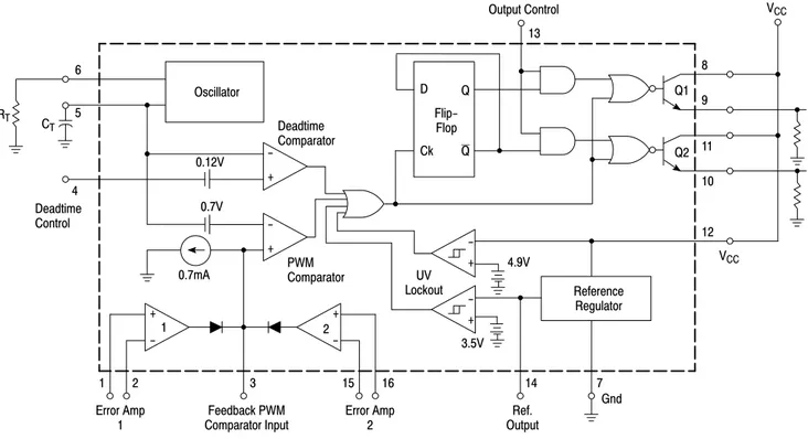
Figure 1. Representative Block Diagram
Figure 2. Timing Diagram
6
RT C T
5
4 Deadtime Control
Oscillator
0.12V
0.7V
0.7mA
+ 1 −
− +
− +
+ 2
−
D Q
Ck
− +
+ −
3.5V 4.9V
13
Reference Regulator
Q1
Q2 8
9
11
10
12 VCC
VCC
1 2 3 15 16 14 7
Error Amp 1
Feedback PWM Comparator Input
Ref. Output
Gnd UV
Lockout Flip− Flop
Output Control
Error Amp 2 Deadtime Comparator
PWM Comparator
Q
Capacitor CT
Feedback/PWM Comp. Deadtime Control
Flip−Flop Clock Input
Flip−Flop Q
Flip−Flop Q
Output Q1 Emitter
Output Q2 Emitter
Output Control
APPLICATIONS INFORMATION
Description
The TL494 is a fixed−frequency pulse width modulation
control circuit, incorporating the primary building blocks
required for the control of a switching power supply. (See
Figure 1.) An internal−linear sawtooth oscillator is
frequency− programmable by two external components, R
Tand C
T. The approximate oscillator frequency is determined
by:
fosc≈ 1.1
RT• CT
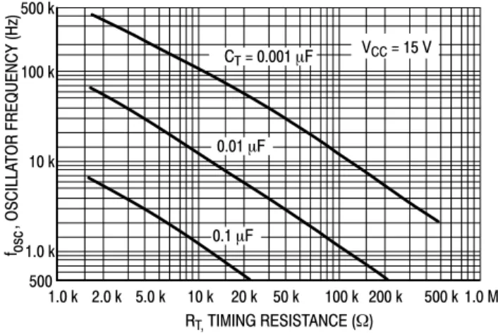
For more information refer to Figure 3.
Output pulse width modulation is accomplished by
comparison of the positive sawtooth waveform across
capacitor C
Tto either of two control signals. The NOR gates,
which drive output transistors Q1 and Q2, are enabled only
when the flip−flop clock−input line is in its low state. This
happens only during that portion of time when the sawtooth
voltage is greater than the control signals. Therefore, an
increase in control−signal amplitude causes a corresponding
linear decrease of output pulse width. (Refer to the Timing
Diagram shown in Figure 2.)
The control signals are external inputs that can be fed into
the deadtime control, the error amplifier inputs, or the
feedback input. The deadtime control comparator has an
effective 120 mV input offset which limits the minimum
output deadtime to approximately the first 4% of the
sawtooth−cycle time. This would result in a maximum duty
cycle on a given output of 96% with the output control
grounded, and 48% with it connected to the reference line.
Additional deadtime may be imposed on the output by
setting the deadtime−control input to a fixed voltage,
ranging between 0 V to 3.3 V.
Functional Table
Input/Output
Controls Output Function
fout fosc = Grounded Single−ended PWM @ Q1 and Q2 1.0
@ Vref Push−pull Operation 0.5
The pulse width modulator comparator provides a means
for the error amplifiers to adjust the output pulse width from
the maximum percent on−time, established by the deadtime
control input, down to zero, as the voltage at the feedback
pin varies from 0.5 V to 3.5 V. Both error amplifiers have a
common mode input range from −0.3 V to (V
CC− 2V), and
may be used to sense power−supply output voltage and
current. The error−amplifier outputs are active high and are
ORed together at the noninverting input of the pulse−width
modulator comparator. With this configuration, the
amplifier that demands minimum output on time, dominates
control of the loop.
When capacitor C
Tis discharged, a positive pulse is
generated on the output of the deadtime comparator, which
clocks the pulse−steering flip−flop and inhibits the output
transistors, Q1 and Q2. With the output−control connected
to the reference line, the pulse−steering flip−flop directs the
modulated pulses to each of the two output transistors
alternately for push−pull operation. The output frequency is
equal to half that of the oscillator. Output drive can also be
taken from Q1 or Q2, when single−ended operation with a
maximum on−time of less than 50% is required. This is
desirable when the output transformer has a ringback
winding with a catch diode used for snubbing. When higher
output−drive currents are required for single−ended
operation, Q1 and Q2 may be connected in parallel, and the
output−mode pin must be tied to ground to disable the
flip−flop. The output frequency will now be equal to that of
the oscillator.
The TL494 has an internal 5.0 V reference capable of
sourcing up to 10 mA of load current for external bias
circuits. The reference has an internal accuracy of
$
5.0%
with a typical thermal drift of less than 50 mV over an
operating temperature range of 0
°
to 70
°
C.
Figure 3. Oscillator Frequency versus Timing Resistance
500 k
100 k
10 k
1.0 k 500
1.0 k 2.0 k 5.0 k 10 k 20 k 50 k 100 k 200 k 500 k 1.0 M RT, TIMING RESISTANCE (W)
, OSCILLA
T
OR FREQUENCY
(Hz)
f osc
VCC = 15 V
0.01 mF
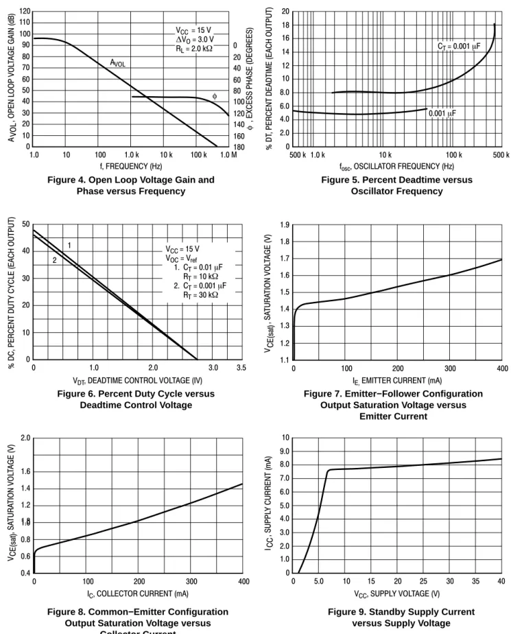
Figure 4. Open Loop Voltage Gain and Phase versus Frequency
Figure 5. Percent Deadtime versus Oscillator Frequency
Figure 6. Percent Duty Cycle versus Deadtime Control Voltage
1.0 10 100 1.0 k 10 k 100 k 1.0 M
, OPEN LOOP
VOL
TA
GE GAIN (dB)
VOL
f, FREQUENCY (Hz) AVOL 0 20 40 60 80 100 120 140 160 180
, EXCESS PHASE (DEGREES)
φ
φ
VCC = 15 V
DVO = 3.0 V
RL = 2.0 kW
A
Figure 7. Emitter−Follower Configuration Output Saturation Voltage versus
Emitter Current
500 k 1.0 k 10 k 100 k 500 k fosc, OSCILLATOR FREQUENCY (Hz)
% DT
, PERCENT
DEADTIME (EACH OUTPUT)
CT = 0.001 mF
0.001 mF
0 1.0 2.0 3.0 3.5
VDT, DEADTIME CONTROL VOLTAGE (IV)
% DC, PERCENT
DUTY
CYCLE (EACH OUTPUT)
VCC = 15 V
VOC = Vref
М1.CT = 0.01 mF
М2.RT = 10 kW
М2.CT = 0.001 mF
М2.RT = 30 kW
2 1
Figure 8. Common−Emitter Configuration Output Saturation Voltage versus
Collector Current
0 100 200 300 400
IE, EMITTER CURRENT (mA)
, SA TURA TION VOL TAGE (V) CE(sat) V
0 100 200 300 400
IC, COLLECTOR CURRENT (mA)
CE(sat) , SA TURA TION VOL TAGE (V) V
Figure 9. Standby Supply Current versus Supply Voltage
0 5.0 10 15 20 25 30 35 40
CC
, SUPPL
Y
CURRENT
(mA)
VCC, SUPPLY VOLTAGE (V)
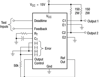
Figure 10. Error−Amplifier Characteristics Figure 11. Deadtime and Feedback Control Circuit
Figure 12. Common−Emitter Configuration Test Circuit and Waveform
+
+ Vin
Error Amplifier Under Test
Feedback Terminal
(Pin 3)
Other Error Amplifier Vref
VCC = 15V
150 2W
Output 1
Output 2 C1
E1
C2 E2
Ref Out Gnd Output Control (+)
(+) (−) (−) Feedback Deadtime
Error VCC
Test Inputs
50k
RT
CT
150 2W
Figure 13. Emitter−Follower Configuration Test Circuit and Waveform
RL
68 VC
CL 15pF C
E Q Each
Output Transistor
15V
90% VCC
10%
90%
10%
tr tf
RL
68
VEE
CL
15pF C
E Q Each
Output Transistor
15V
90%
VEE
10%
90%
10%
tr tf
−
−
Figure 14. Error−Amplifier Sensing Techniques
Figure 15. Deadtime Control Circuit Figure 16. Soft−Start Circuit
Figure 17. Output Connections for Single−Ended and Push−Pull Configurations
VO To Output
Voltage of System R1
1
2 Vref
R2
+ Error Amp
Positive Output Voltage
VO = Vref М1 +
R1
3
+ 1
2
Vref
R2
VO
R1 Negative Output Voltage
−
To Output Voltage of System Error
Amp −
VO = Vref
R1
R1 R2 Output
Control
Output Q
RT CT
DT
Vref
4
5 6
0.001 30k
R1
R2
Max. % on Time, each output ≈ 45 − 80
1 +
Output Q
Vref
4 DT
CS
RS
Output Control
Single−Ended
Q1
Q2
QC
1.0 mA to 500 mA
QE
2.4 V ≤ VOC ≤ Vref
Push−Pull Q1
Q2
C1
E1
C2
E2
1.0 mA to 250 mA Output
Control
0 ≤ VOC ≤ 0.4 V
C1
E1
C2
E2
R2
R2
L1 − 3.5 mH @ 0.3 A
T1 − Primary: 20T C.T. #28 AWG
T1 − Secondary: 12OT C.T. #36 AWG
T1 − Core: Ferroxcube 1408P−L00−3CB
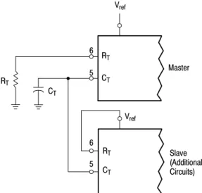
Figure 18. Slaving Two or More Control Circuits Figure 19. Operation with Vin > 40 V Using External Zener
Figure 20. Pulse Width Modulated Push−Pull Converter
RT
CT
6
5 Vref
RT
CT
Master
Vref
Slave (Additional Circuits) RT
CT 5 6
Vin > 40V
RS
VZ = 39V
1N975A VCC
5.0V Ref 12
270 Gnd
7
+Vin = 8.0V to 20V
1
2
3
15
16 +
−
−
+ Comp
OC VREF DT CT RT Gnd E1 E2
13 14 4 5 6 7 9 10 1M
33k
0.01 0.01
VCC
C1
C2
8
11 47
47
10 +
10k 4.7k
4.7k 15k
Tip 32
+ T1
1N4934
L1
1N4934
240
+ 50 35V 4.7k
1.0 22
k +
+VO = 28 V
IO = 0.2 A
12
All capacitors in mF
TL494
0.001
50 35V 50
25V Tip 32
Test Conditions Results
Line Regulation Vin = 10 V to 40 V 14 mV 0.28%
Load Regulation Vin = 28 V, IO = 1.0 mA to 1.0 A 3.0 mV 0.06%
Figure 21. Pulse Width Modulated Step−Down Converter
+Vin = 10V to 40V Tip 32A
1.0mH @ 2A
+VO = 5.0 V
IO = 1.0 A
50 10V +
5.1k MR850
0.1 150
5.1k 5.1k
47k
1.0M 0.1
3 2
1 14
15
16 Comp
−
+
− Vref
+
VCC C1 C2
50 50V
0.001
5 6 4 13 7 9 10
CT RT D.T. O.C. Gnd E1 E2
+
47k
+ 500 10V 150
47
11 12
8
TL494
Test Conditions Results
Line Regulation Vin = 8.0 V to 40 V 3.0 mV 0.01%
Load Regulation Vin = 12.6 V, IO = 0.2 mA to 200 mA 5.0 mV 0.02%
Output Ripple Vin = 12.6 V, IO = 200 mA 40 mV pp P.A.R.D.
Short Circuit Current Vin = 12.6 V, RL = 0.1 W 250 mA
PACKAGE DIMENSIONS
SOIC−16 D SUFFIX
CASE 751B−05 ISSUE J
NOTES:
1. DIMENSIONING AND TOLERANCING PER ANSI Y14.5M, 1982.
2. CONTROLLING DIMENSION: MILLIMETER. 3. DIMENSIONS A AND B DO NOT INCLUDE
MOLD PROTRUSION.
4. MAXIMUM MOLD PROTRUSION 0.15 (0.006) PER SIDE.
5. DIMENSION D DOES NOT INCLUDE DAMBAR PROTRUSION. ALLOWABLE DAMBAR PROTRUSION SHALL BE 0.127 (0.005) TOTAL IN EXCESS OF THE D DIMENSION AT MAXIMUM MATERIAL CONDITION.
1 8
16 9
SEATING PLANE
F
J M
RX 45_ G
8 PL P −B− −A−
M
0.25 (0.010) B S
−T−
D
K
C
16 PL
S
B
M
0.25 (0.010) T A S
DIM MIN MAX MIN MAX
INCHES MILLIMETERS
A 9.80 10.00 0.386 0.393
B 3.80 4.00 0.150 0.157
C 1.35 1.75 0.054 0.068
D 0.35 0.49 0.014 0.019
F 0.40 1.25 0.016 0.049
G 1.27 BSC 0.050 BSC
J 0.19 0.25 0.008 0.009
K 0.10 0.25 0.004 0.009
M 0 7 0 7
P 5.80 6.20 0.229 0.244
R 0.25 0.50 0.010 0.019
PACKAGE DIMENSIONS
PDIP−16 N SUFFIX
CASE 648−08 ISSUE T
NOTES:
1. DIMENSIONING AND TOLERANCING PER ANSI Y14.5M, 1982.
2. CONTROLLING DIMENSION: INCH. 3. DIMENSION L TO CENTER OF LEADS
WHEN FORMED PARALLEL. 4. DIMENSION B DOES NOT INCLUDE
MOLD FLASH.
5. ROUNDED CORNERS OPTIONAL.
−A−
B
F C
S
H G
D
J
L
M
16 PL
SEATING
1 8
9 16
K
PLANE −T−
M
A
M
0.25 (0.010) T
DIM MIN MAX MIN MAX
MILLIMETERS INCHES
A 0.740 0.770 18.80 19.55
B 0.250 0.270 6.35 6.85
C 0.145 0.175 3.69 4.44
D 0.015 0.021 0.39 0.53
F 0.040 0.70 1.02 1.77
G 0.100 BSC 2.54 BSC
H 0.050 BSC 1.27 BSC
J 0.008 0.015 0.21 0.38
K 0.110 0.130 2.80 3.30
L 0.295 0.305 7.50 7.74
M 0 10 0 10
ON Semiconductor and are registered trademarks of Semiconductor Components Industries, LLC (SCILLC). SCILLC reserves the right to make changes without further notice
to any products herein. SCILLC makes no warranty, representation or guarantee regarding the suitability of its products for any particular purpose, nor does SCILLC assume any liability arising out of the application or use of any product or circuit, and specifically disclaims any and all liability, including without limitation special, consequential or incidental damages. “Typical” parameters which may be provided in SCILLC data sheets and/or specifications can and do vary in different applications and actual performance may vary over time. All operating parameters, including “Typicals” must be validated for each customer application by customer’s technical experts. SCILLC does not convey any license under its patent rights nor the rights of others. SCILLC products are not designed, intended, or authorized for use as components in systems intended for surgical implant into the body, or other applications intended to support or sustain life, or for any other application in which the failure of the SCILLC product could create a situation where personal injury or death may occur. Should Buyer purchase or use SCILLC products for any such unintended or unauthorized application, Buyer shall indemnify and hold SCILLC and its officers, employees, subsidiaries, affiliates,