A Remote Demonstrator for Dynamic FPGA Reconfiguration
Hugo Marques
Faculdade de Engenharia
Universidade do Porto
ee06273@fe.up.pt
Jo˜ao Canas Ferreira
INESC TEC and Faculdade de Engenharia
Universidade do Porto
jcf@fe.up.pt
Abstract
This paper presents a demonstrator for partial reconfig-uration of FPGAs applied to image processing tasks. The main goal of the project is to develop an environment which allows users to assess some of the advantages of using dy-namic reconfiguration. The demonstration platform is built around a Xilinx Virtex-5 FPGA, which is used to implement a chain of four reconfigurable filters for processing images. Using a graphical interface, the user can choose which fil-ter goes into which reconfigurable slot, submit images for processing and visualize the outcome of the whole process.
1. Introduction
Partial dynamic reconfiguration consists in adapting generic hardware in order to accelerate algorithms or por-tions of algorithms. It is supported by a General-Purpose Processor (GPP) and reconfigurable hardware logic [1]. The processor manages the tasks running in hardware and the reconfiguration of sections of the FPGA. In addition, it also handles the communication with external devices.
It is expected that this technology will be more and more present in everyday devices. Therefore, it is important to introduce reconfigurable computing to electronic and com-puter engineering students. The goal of the project is to build a tool to support teaching the fundamentals of dy-namic reconfiguration, as a starting point for students to experiment and be motivated to begin their on research on this field. To emphasize the dynamic reconfiguration oper-ations, a system capable of processing images was imple-mented. In this way the user can easily visualize the results of the whole process.
The basic hardware infrastructure contains a processing chain with four filters working as reconfigurable partitions of the system. In regular operation, images flow through the four filters in sequence. To select the filters and to visu-alize the results of the selected operation, a remote graph-ical user interface was implemented in the Java program-ming language. This interface allows the user to send re-configuration orders to the board in which the system is implemented. The user is able to visualize the original sub-mitted image and the result after the process. As this appli-cation emphasizes the advantage of using dynamic recon-figuration, the remote user interface also shows some
per-formance indicators. The system can be used in two differ-ent ways: a basic use and an advanced use. In the first one, the user only uses the graphical interface and the available filter library. An advanced user can expand the system by developing and implementing new filters following a guide that describes the design flow and the rules for a successful implementation.
The board chosen for the implementation of the system was the Xilinx ML505, which has a Virtex-5 FPGA [2]. The on-board software to control the reconfiguration cess and the image processing tasks runs on a soft-core pro-cessor (MicroBlaze) inside the FPGA. This software was developed using the Embedded Development Kit (EDK) tool by Xilinx. The graphical user interface (GUI) runs in any environment that supports the Java language.
This document describes the approach used and the re-sults obtained in the development of this project, which is mainly focused on a teaching context.The next section talks about work that has been developed in the scope dynamic reconfiguration on demand and dynamic reconfiguration systems with teaching purposes. The other sections of this article describe an overall view of the system (Sect. 3), the approach of hardware that was developed (Sect. 4), the strategies that were used to implement image filters (Sect. 5), the software that was developed for the whole system (Sect. 6), and the results (Sect. 7). Section 8 presents some conclusions.
2. Related Work
The use of dynamic reconfiguration is directly con-nected with its ability to speed up computing. It has al-ready been proved that this kind of technology is capable of producing significant performance improvements in nu-merous applications. Also, the use of dynamic reconfigu-ration enables the reduction of the number of application-specific processors inside a single device, opening the way to weight and power consumption reductions in many ar-eas, like for example a car or a cell phone.
In the scope of reconfiguration-on-demand, a project was developed in 2004, whose main objective was to incor-porate many car functionalities in a single reconfigurable device [3]. As there was no need to have all the function-alities working at the same time, the main approach was to have them multiplexed to save energy efficiently. Algo-rithms were developed to do the exchange between tasks according to the run-time needs and energy efficiency
con-siderations.
This project concluded that systems of this kind are vi-able for the non-critical functionalities of a car, like air con-ditioning, radio, and lights control. It was possible to have four tasks working simultaneously in the FPGA and do ex-changes with others as needed, without compromising the purpose of any activity and saving power consumption and space.
In the scope of demonstrating dynamic reconfiguration of FPGAs for education proposes, a system was recently developed whose main goal is to help students learn the fundamentals of this technology, allowing them to do ex-periments with a base system applied to video processing [4]. This system consists of a video stream that runs from a computer through a Virtex ML506 and back to the com-puter. The bitstreams are loaded at start-up to the board’s internal memory. There are two bitstreams available cor-responding to two possible implementations for transcod-ing the stream: up-scaltranscod-ing the stream to 256×256 pixels or broadcasting the input video stream to four lower quality receivers.
The downloading of the bitstreams into FPGA mem-ory is done through the ICAP. In this specific project, the student experience has two phases: elaborating and imple-menting a C application to run on the MicroBlaze with the goal of transferring the bitstreams for the board, and re-ceiving and executing reconfiguration orders. The second phase is about the user controlling the function, that is be-ing executed in the board, by sendbe-ing reconfiguration re-quests through a serial connection.
In the system that we developed, the user has a graphical interface in which he can choose and send reconfiguration requests to the board and visualize the results before and after processing.
3. Base System Overview
The implementation of the whole system has three parts: software developed for the remote interface, software de-veloped for the soft-core processor and the hardware in-frastructure compsed of the reconfigurable areas and the support hardware (CPU, DMA controller, ICAP, memory interfaces). Figure 1 represents the information flow and the modules used in the system. The reconfigurable hard-ware module is called Img process. The communica-tion between the interface and the board Virtex ML505 is done using TCP/IP sockets.
The soft-core processor is the center and brain of the system. It receives information and commands through the Ethernet module and acts accordingly. Before being pro-cessed, the image that the user sends, is stored on DDR2 RAM memory and then, when the image has been com-pletely received, it is transferred to the processing module Img process. This transfer is done with Direct Memory Access (DMA) [5] module which, when the information is processed, does the same operation in the reverse direction as well.
The Img process module is pipelined and has the four partitions connected in series. This means that four
Figure 1. System overview.
Figure 2. Top module Img process.v slots, each one with the correspondent filter selected by the user, are working simultaneously over successive bands of the image. When the DMA transfers a portion of the image, the module immediately starts processing and puts all pro-cessed bytes in a output memory for the DMA to transfer back again do DDR2 memory. This procedure is repeated until the image has been totally processed.
The partial bitstreams to reconfigure Img process are stored in a flash memory card. This card is read using the SysAce module and the bitstream is sent to the Internal Ac-cess Configuration Point (ICAP) [6] by the control program running on the MicroBlaze processor. The ICAP is respon-sible for writing to the FPGA memory reserved to partial reconfiguration. All these modules are connected by the Processor Local Bus (PLB) [7].
4. Image Processing Hardware
As figure 2 shows, the module Img process has four sub-modules. These are all generated by Xilinx Platform Studio when building the base system. They are respon-sible for the reset of the system, and the communication with the PLB bus. The interrupt control is not used in this version of the project, but it was maintained for future de-velopments.
process-Figure 3. Implemented user logic block digram view. ing logic is implemented. It is here that the four
recon-figurable partitions are instantiated as black-boxes. This module receives collections of bytes with a rate which de-pends on the performance of the DMA and MicroBlaze. The transfer is done via PLB bus, hence with an input and output of four bytes in parallel in every clock cycle.
The chain of filters receives one data byte at a time. Therefore, it is necessary to convert the four bytes received in parallel to a byte sequence (parallel-to-serial converter) . There is also the need to aggregate the result information in a 4-byte word to be sent to the DDR2 memory. Hence, se-rialization and de-sese-rialization modules were placed before and after the filters chain respectively. Figure 3 shows a more detailed view of the implemented user logic.v.
In addition to the modules already mentioned, the img process module contains performance counters, parameters, a stop process system, two FIFO memories, a state machine and the sequence of reconfigurable filters. The performance counters measure how many clock cycles are needed to process the whole image. The parameters block represents the registers used to store values intro-duced by the user through the graphical interface. These parameters are inputs of the user-designed filters and can be used in many ways. For example, the input parameter of one filter can be used as the threshold value. The two FIFO memories are used to store received and processed data. The finite state machine controls the whole opera-tion: it has as inputs all the states of the other modules and acts according to them. The stop module prevents the sys-tem from losing data: when the Fifo OUT memory is full, the system stops, or, when the Fifo IN is empty and the last byte has not yet been received, the system stops. The system resumes processing when Fifo OUT memory has
space available for storing new results and Fifo IN mem-ory has new bytes to be processed.
The filter chain consists in four filters connected in se-quence by FIFO memory structures. In overall there are eight FIFO memories, two behind each filter, as Figure 4 shows. In a given filter, the most current line of the image, is passed directly to the next filter and, at the same time, is updating the middle FIFO memory. Also, the bytes that were previously in the middle FIFO are entering the upper FIFO memory. In this way, every time a line is processed, the upper FIFO memory has the older line (N-2), the mid-dle FIFO has the second to last line (N-1) and the most re-cent line (N) enters the filter directly. This arrangement en-sures that the filter block receives successive columns of a three-line memory band. This means, that point operations based on a 3×3 neighborhood can be easily implemented in each filter block.
5. Partial Reconfiguration
5.1. Filter Development
As Fig. 4 shows, the system devised for this work al-lows the user to include new image filters based on point and neighbourhood (3×3) operations. Every filter devel-oped for this infrastructure should have its inputs stored in registers inside the filters. This will decrease the possibil-ity of timing violations on place and route phase. Since the filter has three inputs for bytes from three different image lines, in order to perform local operations the filters should register the incoming image byte, so that the three previous bytes, from each line at a given moment, are stored.
Figure 4. Single filter image process mechanism.
Figure 5. RTL schematic of a 3x3 operation window. they enter the pipeline. Therefore, output calculations on a 3×3 window must also be done in a pipelined fashion, so as to not stall the filter pipeline: in each cycle a new output result must be produced. Hence, the operation is divided in sequential parts with registers between them. This will cause an initial delay at the output, but will not affect the overall frequency of the system. Instead, it will enable the utilization of higher frequencies and decrease timing viola-tions such as hold and setup times.
To implement a 3×3 window like the one shown in Fig. 4, it is necessary to have nine bytes available at a given clock cycle. Hence, nine registers grouped in three shift chains are needed. Figure 5 shows how this arrangement is translated into an RTL schematic. At each cycle, the data for calculations related to the middle pixel (w5) are available. If these operations take longer than the cycle time, they too must be pipelined.
5.2. Floorplanning
The floorplanning [8] [9] phase is done using the Xilinx Planahed tool. Here, the netlists of the filters developed are added to the partitions defined as reconfigurable and then a placement and routing of all the system logic is performed. Finally, the partial and global bitstreams of the system are
generated.
6. Communication and Control Software
To allow the user to control the operations done on the board, a remote graphical interface was developed. The communication between the board and the interface is done with the help of a TCP/IP-based protocol implemented on both sides. The protocol implemented starts out with the interface sending a configuration frame. This frame has all the information about the selected filters, the image size, the parameters for each filter and if it’s a hard or soft pro-cessing request.
If the user chooses to run the process in hardware, the processing is done by the Img process module. If the user chooses the software version, the image processing is done in the soft-core with the implemented software filters. After user approval, the graphical interface sends the whole image and then waits while the board is processing. When the board finishes, the image is sent back to the graphical interface and a new window pops out showing the outcome image.
On the board side, the protocol was implemented us-ing MicroBlaze soft-core and the lwiplibrary provided by Xilinx. When the image is received, a state machine starts sending and retrieving portions of the image to/from the Img processmodule. In the case of software process-ing, the soft-core itself begins processing the image using filters implemented in the C language and compiled with gcc(-O2 optimization level).
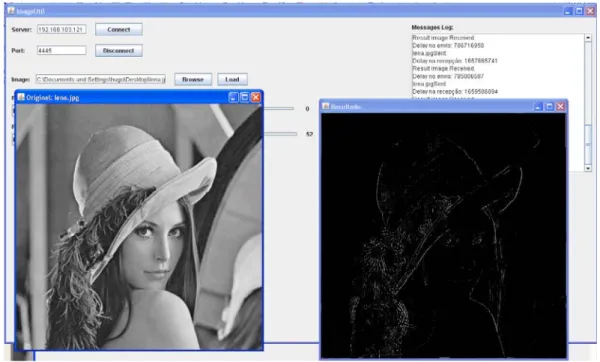
Using the graphical user interface it is possible for the user to configure the connection settings, send an image to process, choose the filters he wants to use and see the im-age that results from the whole process. Besides the visual result, the user is also able to see the measured time that was needed to process the image. In this way, it is possible to do comparisons between software and hardware runs.
The user is allowed to perform any number of execution runs. Every time the user selects a different set of filters, the filter slots that change are reconfigured with the bit-stream corresponding to the user’s choice. Unused slots are configured with a pass-through (“empty”) filter that the user chooses in the graphical interface. Figure 6 shows the
Figure 6. GUI with original and processed image.
Figure 7. Graphical user interface.
interface with one image and the resulting image after pro-cessing, and Fig. 7 shows a snapshot of the interface devel-oped;
7. Results
The soft-core (MicroBlaze) and the Img process core are running at 125 MHz. To measure the performance of the implemented system, some operations with different image sizes were performed and the results were compared to the same chain of processing in Matlab, running on a Intel(R) Core(TM)2 Duo CPU E4500 at 2.2 GHz. Table 1 shows the processing time per pixel for different images.
There are two indicators for the hardware operation (Img process”): total time and effective time. To-tal time is time taken by the whole operation, including the time that DMA spends transferring portions of the image. Effective time accounts only for the time when Img processis actually processing image data.
Table 1. Performance indicators. Img processtime Matlab Image Size Total Effective Total Time
512 x 512 124.86 ns 8.13 ns 54.55 ns 875 x 700 127.80 ns 8.10 ns 102.69 ns 1024 x 1024 129.03 ns 8.06 ns 189.40 ns
Examining Tab. 1 it is possible to conclude that as the image size grows, the processing time per pixel in Matlab increases significantly, but stays approximately constant for the hardware implementation. This can be explained by the pipelined architecture, which processes the image with the four filters working simultaneously. It is also possi-ble to conclude that, as the image size grows, the effective time tends to 8 ns, which is the period that corresponds to the 125 MHz clock frequency. This is also a consequence of the pipelined architecture, which introduces some initial delays, but does not affect the overall frequency. So, as the image gets bigger these delays become more insignificant. The use of other type of filters only affects the initial delay of the pipeline (depending on the hardware complexity of the filter), but does not affect the performance of the whole operation.
Knowing that the system was implemented in a Xilinx XC5VLX50T FPGA device, the resources that were occu-pied were: 33% of registers, 32% of LUTs, 63% of slices, 48% of IOBs and 66% of BlockRAMs. This means that there is room for future developments and improvements.
8. Conclusion
The implementation meets the initial objectives and is completely functional. The user is capable of submitting an image, choosing the filters and parameters he wants to use, run the process and visualize the processed image and performance indicators.
It is possible to enlarge the window for local image op-eration. For that to be accomplished it is necessary to add some more memory FIFOs before each filter. Given the number of BRAM blocks available after implementation, it would be feasible to use an 8×8 window for image process-ing. Adding a new filter to the chain will not degrade the overall performance of the system. However, FPGA rout-ing will be more congested and could lead to a reduction in operating frequency.
In order to enhance and improve the demonstration of the FPGA dynamic reconfiguration capabilities, we aim for future developments in the graphical interface, such as adding animations which can provide a quick understand-ing of what’s happenunderstand-ing in the FPGA durunderstand-ing the reconfigu-ration process. Also, to simplify the development and addi-tion of user-customized filters, a mechanism, provided by the graphical interface as well, could be developed to au-tomatically do the integration, in the design, of a Verilog description filter done by the user; a filter would be then immediately available for further usage. As a result, we would have an automated process able to read a Verilog module description of a filter, synthesize it, implement it in the design’s floorplan and generate a partial bitstream of it. In this way the user would have an easier understanding of the reconfiguration and would be able to have available his own filters to use in the implemented design just by writing a Verilog description of it.
Acknowledgments This work was partially funded by the European Regional Development Fund through the COMPETE Programme (Operational Programme for Competitiveness) and by national funds from the FCT–Fundac¸˜ao para a Ciˆencia e a Tecnologia (Portuguese Foundation for Science and Technology) within project FCOMP-01-0124-FEDER-022701.
References
[1] Pao-Ann Hsiung, Marco D. Santambrogio, and Chun-Hsian Huang. Reconfigurable System Design and Verification. CRC Press, February 2009.
[2] Xilinx Inc. Virtex-5 Family Overview, October 2011. [3] Michael Ullmann, Michael Hubner, Bjorn Grimm, and
Jur-gen Becker. An FPGA run-time system for dynamical on-demand reconfiguration. In Proceedings of the 18th In-ternational Parallel and Distributed Processing Symposium (IPDPS’04), 2004.
[4] Pierre Leray, Amor Nafkha, and Christophe Moy. Implemen-tation scenario for teaching partial reconfiguration of FPGA. In Proc. 6th International Workshop on Reconfigurable Com-munication Centric Systems-on-Chip (ReCoSoC), Montpel-lier, France, June 2011.
[5] Xilinx Inc. LogiCORE IP XPS Central DMA Controller (v2.03a), December 2010.
[6] Xilinx Inc. LogiCORE IP XPS HWICAP (v5.01a), July 2011. [7] Xilinx Inc. LogiCORE IP Processor Local Bus (PLB) v4.6
(v1.05a), September 2010.
[8] Xilinx. PLanahead Software Tutorial, Design Analysis And Floorplanning for Performance. Xilinx Inc, September 2010. [9] P. Banerjee, S. Sur-Kolay, and A. Bishnu. Floorplanning in modern FPGAs. In 20th International Conference on VLSI Design, 2007., pages 893 –898, January 2007.