Surface Morphological Studies of Solar Absorber Layer
Cu
2ZnSnS
4(CZTS) Thin Films by Non-vacuum Deposition Methods
Chandra Sekhar Kanuru
1,*, G.L. Shekar
2, L. Krishnamurthy
3, R. Gopal Krishne Urs
41
Centre for Nano-Technology, The National Institute of Engineering, Mysore, India
2
Department of Industrial & Production Engineering, The National Institute of Engineering, Mysore, India
3
Department of Mechanical Engineering, The National Institute of Engineering, Mysore, India
4
Department of Physics, The National Institute of Engineering, Mysore, India
(Received 06 February 2014; revised manuscript received 02 June 2014; published online 20 June 2014)
The consumption of fossil fuel globally has been enormous and has reached an alarming rate resulting in fast depletion of the available resources and at the same time polluting the environment. Hence there is a growing need to take cognizance of abundant amount of inexpensive energy available in the nature espe-cially solar energy. Development and commercialization of Photovoltaics has been in focus due to its low cost, high absorption coefficient and suitable direct band gap for solar energy conversion applications. An attempt has been made in this work to synthesize the CZTS thin films by Electro deposition and Sol-gel method on Indium Tin Oxide (ITO) glass and Soda Lime Glass( SLG) substrates respectively. CZTS thin films have been prepared using a 3-stage electro chemical system wherein the precursors are deposited us-ing platinum foil as a counter electrode and AgCl electrode as a reference electrode and Sol gel method. Surface morphology and optical properties have been studied using Atomic Force Microscopy, Scanning Electron Microscopy, X-ray Diffractometer and UV-Vis Spectroscopy
Keywords: CZTS, Thin film photovoltaics (PV’s) electro deposition, Surface morphological studies.
PACS numbers: 68.35.bj, 68.55. – a, 78.55.Hx,
81.15. – z, 84.60.Jt
*
[email protected]
1.
INTRODUCTION
The use of thin film Photo Voltaic (PV) devices for
so-lar energy applications is rapidly increasing. The
effi-ciencies obtained by employing different thin films like
CIGS [Cu(In,Ga)S
2] and CIGSe [Cu(In, Ga)Se
2], CuInSe
(CIS), CdTe have already reached their optimum levels
[1]. Also they contain rare materials like indium and
gallium which are expensive and toxic [2]. The CZTS is a
kesterite quaternary semiconductor which contains
ele-ments that are not toxic and are abundantly available on
earth. In addition, it has an appropriate optical band gap
~ 1.50 eV and absorption coefficient of 104 cm
– 1for solar
cell applications [3]. Due to this, Cu
2ZnSnSe
4(CZTSe),
Cu
2ZnSnS
4(CZTS) solar absorbers have gained
atten-tion for their potential applicaatten-tion in non silicon based
Photovoltaic cells [4]. It has been mentioned in literature
that the CZTS solar absorbers which were synthesized
using different methods such as thermal evaporation,
sputtering technique and electrodepostion have found to
have reached an efficiency of 5.4 %, 6.7 % and 7.2 % by
evaporation, sputtering and electrodepostion
respective-ly [5, 6, 7]. Even though electronic structure of the
Cu
2ZnSn(S, Se)
4material system has been investigated
theoretically, there is still enough scope to improve the
structure by carrying out experimental investigation [7].
An attempt has been made in this study to improve the
surface morphology of CZTS thin films. Among all the
above mentioned preparation techniques, sol-gel and
electrodepostion possess advantages like low cost and
uniform coatings. These methods are very simple and
without requiring any vacuum system. The main
objec-tive of this work has been to show the possibility of
sol-gel and electrodeposition of Cu
–
Zn
–
Sn alloy followed by
Sulphur as precursor layers and their subsequent
an-nealing in N
2atmosphere. These films have been
ana-lyzed using Scanning Electron Microscope (SEM),
Atom-ic Force MAtom-icroscope (AFM), X-Ray Diffractometer and
UV-Visible Spectroscopy.
2.
EXPERIMENTAL SECTION
While carrying out this work the following materials
viz., Copper (II) Sulfate Pentahydrate (CuSO
4·5H
2O), Zinc
Sulfate Hepthahydrate (ZnSO
4·7H
2O), Tin Sulfate
(SnSO
4) and Sodium Thiosulfate (Na
2S
2O
3), Tri-sodium
Citrate (C
6H
5Na
3O
7) which are of analytical grade have
been considered. The materials pertaining to this study
have been procured from Sigma Aldrich and Rankem
Chemicals. An attempt has been made in the study to
electro deposit a thin film of CZTS on ITO coated glass
substrates using a cyclic voltammetry (CV) of CH
instru-ments USA make.
is 15 minutes The Cyclic voltametry (CV) Curve as shown
figure 1. The sulfurization has been carried out separately
by mixing of Sodium Thiosulfate (0.02 M) in aqueous
solu-tion after deposisolu-tion of CZT for 10 minutes and Hydro
Choric acid (HCl) has been used as pH control solution to
get a pH concentration of 5. The applied potential of CZT
and sulfarization is 0 to
–
1.5 V [8].
-1.6 -1.4 -1.2 -1.0 -0.8 -0.6 -0.4 -0.2 0.0 -0.005 -0.004 -0.003 -0.002 -0.001 0.000 0.001 Sn2+ - Sn
Cu2+ - Cu Sn2+ - Sn
Zn2+ - Zn C u rr e n t/ A Potential/ V CZT CV curve
Fig. 1 –CV curve of CZTS solar absorber
Sol-gel coating was performed at room temperature
using Dip coating technique. Soda lime glass (SLG)
sub-strates were used as a substrate base for CZTS growth.
The stoichiometry of sol solution was optimized by
varia-tion of individual metallic species concentravaria-tions. The
Dip coating was carried out using a sol solution of copper
(II) acetate monohydrate, zinc (II) acetate dihydrate, and
tin (II) chloride dihydrate which are of analytical grade
have been considered. Monoeth
anolamine (≈
5 ml) is
used as stabilizer [9]. The materials pertaining to this
study have been procured from Sigma Aldrich and
Rankem Chemicals. The precursors were dissolved in
25 ml of 2-methoxyethanol. For Dip coating the SLG
substrate was dipped in the sol solution and taken out at
uniform speed and dried at 200
°C. The coating pr
ocess
was repeated four times to obtain the desired thickness
of film. It was observed that the film coated more than
four layers were peeled off after annealing. This is
be-cause the adhesive strength between substrate and film
decreases with increase in thickness. The annealing of
Sol gel coated dried films were carried out at a
tempera-ture of 500
°C for 1
hour.
3.
CHARACTERIZATION OF CZTS SOLAR
ABSORBER
The obtained films were characterized by D2 Phaser
X-ray Diffracotmeter from Bruker Axs, Germany for
Phase transitions, Desktop Scanning Electron
Micrso-cope from Phenom, Netherlands and Atomic Force
Mi-croscope from park Systems, South Korea for Surface
Morphological studies. The Preliminary results are in
well agreement with the established reports
3.1
Structural Characterization
The CZTS thin films prepared by Electrodeposition
and Sol-gel method are annealed at 500 C for one hour
in vacuum furnace to get Crystallinity Sturcuture.
Fig-ure 2a show X-rd peaks CZTS thin film prepared by
Electrodepostion. It can be observed that crystallanity
has been formed after annealing. The structural
prop-erty of CZTS thin films have been analyzed using XRD
measurement with 2 theta scanning from 20 to 80.
It
is observed that all the XRD patterns consist of (112),
(200), (220), (311) and (332) diffraction peaks
corre-sponding to different crystallographic planes of
Cu
2ZnSnS
4suggesting that the films are
polycrystal-line with kesterite crystal structure. The diffraction
20 30 40 50 60 70 80
Cu x Sn y IT O (4 2 0 ) IT O (2 2 2 ) IT O (4 1 1 ) Cu x S C Z T S ( 2 0 0 ) (C u x)(S S nx S) C Z T S ( 2 2 0 ) C Z T S (3 3 2 ) IT O (4 4 0 ) C Z T S (3 1 2 )
CuxS SnyS
C u Zn x (C ux S) C Z T S ( 2 0 0 ) C o u n ts ( A.U ) 2Theta (degree)
CZTS annealed at 500oC
(a)
(b)
Fig 2 –X-rd patterns of CZTS thin film by electrodepositon (a) and Sol gel synthesi (b)
peaks of (411), (420), (440) corresponding to
crystallo-graphic planes of ITO. These results are in agreement
with reported literature [4, 9, and 10]. Furthermore, some
metal sulfide and other secondary phases, such as Cu
x
S,
SnS
xand Cu
xSn
y, have also been detected. These
correspond-ing to different crystallographic planes of Cu
2ZnSnS
4sug-gesting that the films are polycrystalline with kesterite
crystal structure. These results are in agreement with
reported literature [11-13]. Furthermore, some metal
sul-fide and other secondary phases, such as Cu
xS, SnS
xand
Cu
xSn
y, have also been detected. These secondary phases
are often observed in CZTS thin films are copper-rich
chalcopyrite structure.
3.2
Morphological Characterization
The morphology of electrodeposited metal layer and
sol-gel approach is crucial for producing smooth dense
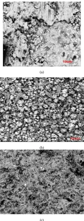
CZTS films. Figures 3a and b show SEM micrographs of
CZTS before and after annealing respectively. At higher
magnification of the image, two distinct gain structures
(a)
(b)
(c)
Fig. 3 –a – before annealing; b – after annealing by Electro deposition; c – after annealing by sol-gel
(a)
(b)
Fig. 4 – AFM Images of Surface Morphology CZTS thin films by Electrodepostion (a) and sol-gel process (b)
viz., spherical and fiber are observed. The average grain
size is found to be 0.8 m
±
0.4 m for spherical grains
and 2.5
±
0.5 m 0.2
±
0.1 m for fiber grains which is
in agreement with the reported literature [14]. Fig. 3c
shows SEM micrographs of CZTS after annealing by
sol-gel. However, the film appears to be quite dense with
few voids and a highly interconnected network of grains.
It is necessary to produce such dense films with good
interconnection between grains for high performance
photovoltaic devices [15].
aver-age film thickness is around 100 nm. From Figure 4b,
the length of the particle is 1.5 m
±
1 m. The average
particle size from 2D AFM images is observed to be
150 nm
±
2 nm. The average film thickness is around
100 nm.
3.3
Band Gap Measurement
Band gap measurements of CZTS thin films have
been carried out using transmittance data obtained
from Shimadzu spectrophotometer equipped with UV
Probe spectrum, software version 2.30. Fig 5a shows
the optical transmittance of Electrodeposited CZTS
thin film annealed at 500
°
C. The percentage
transmit-tance is found to be 13 % i.e. there is more absorption
of photons in CZTS film. For Cu
2ZnSnS
4film, the curve
of absorption coefficient (
hν
)
2vs Energy (
hν
) has been
plotted, as shown in Fig. 5b. The band gap of the
Cu
2ZnSnS
4film was found to be 1.6 eV.
(a)
(b)
Fig. 5– Transmittance of Spectra Band gap calculation of CZTS thin films by Electrodeposition
Fig. 6a shows the optical transmittance of sol-gel
prepared CZTS thin film annealed at 500
°
C of various
thicknesses. The percentage of transmittance is
de-creasing with increase in thickness of the film. For the
annealed dip coated CZTS film at 500
°C, plotted the
graph between Absorption coefficient (
h
ν
)
2vs. Energy
(
hν
) has been shown in Fig. 6b. The band gap of CZTS
film for first coating was found to be 2.5 eV and further
it decreases to 1.7 eV while increasing the thickness of
film which is the desired band gap of CZTS thin film.
The optical band gap is in agreement with the
litera-ture [14]. The obtained optical band gap by Electro
deposition and Sol-Gel suggests that CZTS is suitable
for solar cells.
(a)
(b)
Fig. 6 –Transmittance of Spectra (a) and Band gap calcula-tion (b) of CZTS thin films by sol-gel approach
4.
CONCLUSIONS
re-spectively. It is observed that the average dimensions of
the
fibered
grains
are
approximately
around
2.5
±
0.5 m 0.2
±
0.1 m. In Case of Sol-Gel method,
X-ray diffraction patterns indicate the absence of
crystal-linity formation before annealing. However, the
for-mation of crystallinity is observed after annealing. X-ray
diffraction patterns of CZTS thin films indicate a
kester-ite structure (Copper rich Zinc poor compounds)
includ-ing secondary metal, metal sulfide phases and copper
rich chalcopyrite. It is observed from AFM that the
length of the particle is 1.5 m
±
1 m and the average
particle size is 150 nm
±
2 nm. Film thickness is found to
be 100 nm. The Thickness of the thin films of CZTS
coated on glass substrates are varied. It is observed that
the band gap decreases with increase in film thickness.
Band gap is found to be 1.7 eV. From surface
morpho-logical studies, it can be concluded that the particles
are quite dense and a highly interconnected network of
grains, which is necessary for high performance of
pho-tovoltaic devices.
ACKNOWLEDGEMENTS
This work was financially supported by “Nano Mi
s-sion, Department of Science and Technology,
Govern-ment of India, New Delhi, under the project reference
number SR/NM/NS-43/2010 dated 27-09-2010.
REFERENCES
1. Minlin Jiang, J. Photon. Energ. 1, 019501 (2011).
2. M. Gancheva, L. Kaupmeesa, J. Iliynaa, J. Raudojaa,
O. Volobujevaa, H. Dikovb, M. Altosaara, E. Mellikova,
T. Varemaa, Energ. Procedia 2, 65 (2010).
3. M. Jeona, Y. Tanakab, T. Shimizub, S. Shingubarab,
En-erg. Procedia 10, 255 (2011).
4. Minsung Jeon, Tomohiro Shimizu, Shoso Shingubara,
Mater. Lett. 65, 2364 (2011).
5. Ji Li, Tuteng Ma, Ming Wei, Weifeng Liu, Guoshun Jiang,
Changfei Zhu, Appl. Surf. Sci. 258, 6261 (2012).
6. J.K. Katagiri Hironori, S. Yamada, T. Kamimura,
W.S. Maw, T. Fukano, T. Ito, T. Motohiro, Appl. Phys.
Ex-press 1, 041201 (2008).
7. S. Ahmed, K.B. Reuter, O. Gunawan, L. Guo,
L.T. Romankiw, H. Deligianni, Adv. Energ. Mater.2, 253
(2011).
8. Yanfeng Cui, Shaohua Zuo, Jinchun Jiang,
Sheng-zhao Yuan, Junhao Chu, Sol. Energ. Mater. Sol. C. 95,
2136 (2011).
9. Remigijus, Juskenasn, Stase Kanapeckait Violeta
Karpavicien, Zenius Mockus, Vidas Pakstas, Ausra
Sel-skiene, Raimondas Giraitis, Gediminas Niaura, Sol.
En-erg. Mater. Sol. C. 101, 277 (2012).
10.B.S. Pawar, S.M. Pawar, S.W. Shin, D.S. Choi, C.J. Park,
S.S. Kolekar, J.H. Kim, Appl. Surf. Sci. 257, 1786 (2010).
11.A. Ghazali, Z. Zainal, M.Z. Hussein, A. Kassim, Sol.
En-erg. Mater. Sol. C. 55, 237 (1998).
12.Y. Cui, S. Zuo, J. Jiang, S. Yuan, J. Chu, Sol. Energ.
Ma-ter. Sol. C. 95, 2136 (2011).
13.P. Fernandes, P. Salome, A. Cunha, Thin Solid Films 517,
2519 (2009).
14.R. Schurr, A. Hölzing, S. Jost, R. Hock, T. Vo, J. Schulze,
A. Kirbs, A. Ennaou, M. Lux-Steiner, A. Weber,
I. Kötschau, H.W. Schock, Thin Solid Films 517, 2465
(2009).
15.N. Kamoun, H. Bouzouita, B. Rezig, Thin Solid Films 515,