DOI:
10.2298/SOS0602155P
UDK 539.216:546.74:546.76
Structure and Surface Composition of NiCr Sputtered Thin
Films
S. Petrovi
ć
*), N. Bundaleski, M. Radovi
ć
, Z. Risti
ć
, G. Gligori
ć
, D. Peruško,
S. Zec
Institute of Nuclear Science – Vinca, POB 522, 11001 Belgrade, Serbia
Abstract:
Thin films of nichrome were deposited by d.c. sputtering of a target (80%Ni – 20%Cr w.t.) by Ar+ ions at a working pressure of 10-1 Pa and at room temperature. The phase composition and grain size were studied by X-ray Diffraction (XRD), while the surface chemical composition was determined by Low Energy Ion Scattering (LEIS). Analysis of phase composition showed that the NiCr thin films were a solid solution of chromium in a nickel matrix with increased nickel lattice parameters. LEIS analysis showed the presence of Ni, Cr and O in the first atomic layer. There is a strong suspicion that surface passivation occurred by forming Cr2O3 oxide at the surface.
Keywords: Nichrome thin films, LEIS, XRD.
Introduction
Nichrome (NiCr 80/20 wt.%) is a material with many various applications in different fields such as electronic industry (production of resistor elements) or strain gauge applications. However it is particularly interesting as a protective material in a high temperature oxidizing environment where it becomes passivated [1]. Jeng et al. [2] investigated the passivation of a NiCr alloy by low pressure O2 exposure at room temperature and they proposed that the initial stage of oxidation consists of preferential oxidation of Cr to Cr2O3 although Ni is oxidized more rapidly to NiO than pure Ni under identical exposure conditions. They suggested a model consisting of a layered structure with Ni hydroxide and Cr oxide in the first layer, a mixture of Cr oxide, small amounts of Ni metal and NiO in the next layer, a Cr dopleted layer and NiCr alloy as the lowermost layer. Epling et al. examined initial oxidation of polycrystalline NiCr alloys at different temperatures and effects of subsequent vacuum annealing treatment [3].
In contrast to the mentioned work, in this paper we investigated passivation of nichrome thin films at room temperature in air. Physical and chemical properties of NiCr thin films depend on the formation conditions used in deposition environment. The structure of the sputter deposited nichrome thin film was analyzed using X-ray diffraction (XRD), and the surface composition was determined by low energy ion scattering (LEIS).
________________
Experimental
N
ichrome thin films were deposited by d.c. sputtering of a target (80%Ni – 20%Cr w.t.) by Ar+ ions. The substrates used in the experiment were glass and alumina. A standard cleaning procedure was applied for preparing substrates prior to film deposition. Deposition was performed using a Balzers Sputtron II vacuum system. Acceleration voltage (U = 1.5 kV) and current on the target (I = 0.7 A) were maintained constant during the experiment. Before deposition, the sputtering chamber was evacuated by a turbo molecular pump down to a final pressure of p = 1.33×10⁻³ Pa. The cleaning procedure included electron heating up to the temperature of about 150ºC and afterward Ar+ bombardment for about 2 min. The partial pressure of argon was pAr= 1.33× 10⁻¹ Pa. Under such conditions, the constant deposition rate was 0.14 nms-1. After deposition, the thickness was measured by a Talystep I profilometer. The thickness of NiCr thin films was 880 nm for all substrates used.The phase composition and crystalline structure of NiCr deposits were determined by the X – ray diffraction method using a SIEMENS diffractometer with Cu Kα radiation. Diffractograms were obtained by a powder diffractometer with Ni filtered emission. Angles 2θ in the range 30º to 100º were scanned by steps 0.02º in a time sequence of 1s. Phase identification was made by comparing diffraction patterns with Joint Committee on Powder Diffraction Standards (JCPDS) cards [4].
Crystal sizes (D) were determined applying the corrected Scherrer equation (1):
θ
β
θ
πβ
λ
cos
10
5
,
79
cos
2
10
360
10m
10m
a
D
− −×
=
×
=
(1)where: a is the geometrical coefficient (a = 0.9 for cubic crystals), λis wavelength of the X-ray beam (λCuKα = 1.5418 × 10⁻¹⁰m), 2θ is the reflex of the reference (crystal size larger than
500 nm),
β
=
b
2−
B
2 is corrected line broadening, B is the FWHM of peaks and b is a correction factor [5]. The FWHM values were determined using Gaussian fit and Kα-stripping with a freeware evaluation softwere (Diffrac Plus – BRUNER –axs).Low Energy Ions Scattering (LEIS) experiments were carried out using a setup described in detail elsewere [6]. Ions of He+ in the energy range 1 – 2.5 keV were scattered from a nichrome sample placed in an UHV chamber. The incoming angle ϕ and scattering angle θ could be continuously changed in the range from 0º to 90º. The sample was cleaned by grazing incidence He+ ion beam with the current density of about 3 µA/cm2 or greater, until a steady state was obtained. Surface composition measurements were performed with the incoming and scattering angles of 45° and 90°, respectively. The analyzing He+ ion beam was of the same intensity as in the cleaning procedure, which is enough for maintaing surface cleanliness during the experiment [7]. The working pressure in the chamber was lower than 3×10⁻⁷ Pa.
Results and discussion
In order to make a raw estimation of the thin film composition we calculated the sputtering coefficients of nickel and chromium by 1.5 keV Ar+ ions at normal incidence. The calculations were performed using a SRIM 2003 program [8]. The calculated sputtering coefficient of nickel is 3.61, while that of chromium is 2.61. According to this result the relative concentration of nickel in the thin film could easily exceed 80 %, which is the concentration of the target.
A XRD diffractogram of a NiCr thin film deposited on a glass substrate is presented
2θ = 44.238º which can be the result of overlapping of two peaks corresponding to Ni (111) (2θ = 44.505º from JCPDS card (04-0850)) and Cr (110) (2θ = 44.390º from JCPDS card (06-0694)). On the other hand, the experimental value of the lattice parameter from the XRD diffractogram is a = 0.35493 ± 0.00015 nm.
a)
b)
Fig. 1. XRD diffractograms: a) NiCr thin film; b) pure polycrystalline Ni.
The observed peaks in the NiCr diffractogram are situated approximately at the same position as the peaks in the diffractogram of pure Ni. Peaks of the NiCr thin film difractogram have moved towards lower values of angle 2θ with respect to the peaks in Ni diffractograms, and the discrepancy never exceeds 1 %. The preferred growth orientation of NiCr deposit Ni(111), although other Ni orientations exist as well. NiCr thin films have a polycrystalline structure with a grain size of about 37 nm. XRD results clearly show that nickel dominates in the deposited thin film, which is expected taking into account the calculated sputtering coefficients using TRIM code.
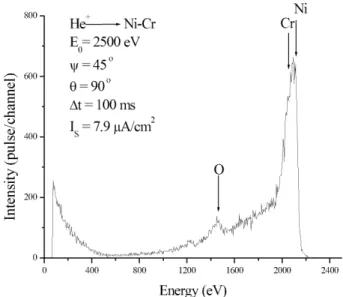
LEIS provides information on the composition with ultimate surface sensitivity. This information is practically restricted to the first atomic layer. Surface cleaning in this type of experiments usually consists of Ar+ ion sputtering and/or sample heating. Both procedures can yield significant changes of the surface composition due to preferential sputtering (in the case of Ar+ bombardment) and surface segregation effects that take place at elevated temperatures. As mentioned already, the sample was cleaned by intense He+ sputtering at a grazing incident angle in order to avoid this problem. The LEIS spectrum of 2.5 keV He+ ions scattered from NiCr thin film is presented in Fig.2. The energies of He+ ions single scattered from Ni and Cr are very close due to the low difference of atom masses. The intensive peak is obtained by overlapping of peaks corresponding to nickel and chromium. This fact hinders quantitative composition characterization. The low energy tail positioned on the left from this peak is a consequence of reionisation effects during He atoms scattering from chromium [9]. Besides the main peak in the spectrum, there is also another one, corresponding to oxygen. Theoretical predictions of peak positions, according to the elastic single collision model, are presented as arrows in Fig. 2.
Fig. 2. LEIS spectrum of He+ ions scattered from the NiCr surface
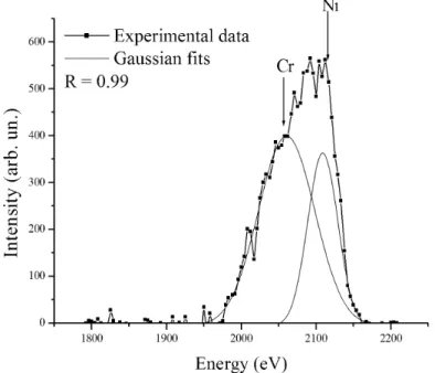
this experimental setup and the same experimental conditions (the same projectile, primary ion energy and the scattering angle) was performed for nickel and an appropriate sensitivity factor ηNi was determined [10]. The surface concentration of nickel can then be calculated from the relation
t
I
S
n
P Ni
Ni
Ni
=
η
∆
, (2)where SNiis the area of the Gaussian corresponding to nickel, IPis the primary beam current and ∆t is the time width of the channel. The calculated concentration of Ni is 2.3ּ1014 cm-2. Unfortunately, a reliable estimation of the relative nickel concentration can not be made because we do not have information on the surface concentrations of Cr and O. However, neutralization of He+ scattered from chromium is far greater that that of He+ scattered from nickel [9], which implies that the sensitivity factor of chromium ηCr < ηNi. In other words, the same signal of chromium and nickel would mean that the surface concentration of chromium is greater. Knowing that the chromium signal is about two times greater than that of nickel, we have a strong suspicion that surface segregation of chromium took place.
Fig. 3. Resolving of overlapped LEIS signals corresponding to nickel and chromium.
Although nickel most likely dominates in the deposited thin film, according to XRD analysis and sputtering coefficient calculations, its concentration in the first atomic layer is low. Taking into account the presence of an oxide phase at the surface and most probable surface segregation of chromium, we assume that Cr2O3, which is the most stable oxide phase of chromium, is present in the first atomic layer of the thin film. This explanation is in accordance with the results presented in [3], where the nichrome alloy was exposed to oxygen at room temperature.
Acknowledgement
References
1. 1.W. S. Epling, G. B. Hoflund, Thin Solid Films 292 (1997) 236.
2. S. P. Jeng, P. H. Holloway, D. A. Asbury, G. B. Hoflund, Surf. Sci. 235 (1990) 175.
3. G. B. Hoflund, W. S. Epling, Thin Solid Films 307 (1997) 126.
4. JCPDS-International Centre for Data(ICDD), PCPDFWIN v. 2.00,1998.
5. H. P. Klug, L.E. Alexander, X – Ray Diffraction Procedures, J. Wiley & Sons,1974.
6. I. Terzić, N. Bundaleski, Z. Rakočević, N. Oklobdžija, J. Elazar, Rev. Sci. Inst., 7 (2000) 4195.
7. N. Bundaleski, P. Bankov, M. Radović, Z. Rakočević, Proceedings of the 21st SPIG, Sokobanja, Yugoslavia, 29 (2002) 218.
8. J.F. Ziegler, J.P. Biersack, U. Littmark, The Stopping and Range of Ions in Solids, Pergamon Press, 1985.
9. S.N. Mikhailov, R.J.M. Elfrink, J.P. Jacobs, L.C.A. van den Oetelaar, P.J. Scanlon, H.H .Brongersma, Nucl. Instr. & Meth. B 93, (1994) 149.
10. N. Bundaleski, PhD thesis, Belgrade University, 2003.
Са р а: Т –
(80%Ni – 20%Cr) Ar+ 10-1 Pa .
–
(XRD), ђ
(LEIS). А NiCr
,
. М LEIS Ni, Cr
. Cr2O3
.