*e-mail: [email protected]
Antilocalization Effect on Photo-Generated Carriers in Semi-Insulating Gaas Sample
Emilson Ribeiro Vianaa, Geraldo Mathias Ribeiroa, Alfredo Gontijo de Oliveiraa,
Marcelos Lima Peresb*, Rero Marques Rubingerb, Carla Patrícia Lacerda Rubingerb
aDepartamento de Física, ICEx, Universidade Federal de Minas Gerais – UFMG,
CP 702, CEP 30123-970, Belo Horizonte, MG, Brasil
bInstituto de Ciências, Departamento de Física e Química, Universidade Federal de Itajubá – UNIFEI,
CP 50, CEP 37500-903, Itajubá, MG, Brasil
Received: September 14, 2011; Revised: April 6, 2012
Magnetoresistance measurements were performed on an illuminated semi-insulating GaAs sample with intrinsic deep level defects. Electrical carriers were photo-generated under light excitation and positive magnetoresistance for B < 0.2 T was observed in the whole range of temperatures measured
(220-315 K). Using the model developed by H. Fukuyama and K. Hoshino, we interpreted the positive magnetoresistance as mainly caused by weak antilocalization effects over hole carriers for T > 240 K.
The high disorder originated from the low temperature growth of the sample leads to the strong localization of carriers and gives rise to the positive magnetoresistance observed at temperatures as high as room temperature.
Keywords: semi-insulating GaAs, deep-level defects, antilocalization
1. Introduction
Electron transport in disordered systems has been widely studied over the past 30 years1-3 and is a powerful tool for probing electron-electron interactions4 and weak localization phenomenon5. For 2D systems, low field positive magnetoresistance has been observed on GaAs based structures and it is attributed to the spin-orbit coupling interaction which could be originated from the electric field of the atomic nucleus or related to the particular characteristics of crystalline and band structure of the solid6-10. Nevertheless, few studies about spin-orbit coupling interaction have been reported on 3D semiconductor thin films6,11,12. One method to determine the strength of the spin-orbit coupling is through the weak anti-localization effect (suppression of weak localization due spin-orbit interactions)1. One can use the models that predict the contribution to the magnetoconductivity due to this effect and obtain the inelastic and spin-orbit scattering times and verify how they respond to the change of temperature or carrier concentration8-10.
In this work, we report on the positive magnetoresistance measured on an illuminated GaAs sample in the temperature region of 220-315 K with intrinsic deep level defects. For the temperatures higher than 240 K, the positive magnetoresistance indicates the presence of spin-orbit coupling over the hole carriers that diffuse in a highly disordered system. The disorder is originated during the growth process where the GaAs material extremely rich in intrinsic deep level defects is obtained by low temperature molecular beam epitaxy (LT- MBE) growth13. This material is used in applications on the development of high quality
Antilocalization Effect on Photo-Generated Carriers in Semi-Insulating Gaas Sample
spin-orbit interaction in a given material is the main key for new advances in spintronics field16, we expect that our work could shed some light on the possibility of using the spin-orbit interaction for the development of room temperature spintronic devices.
2. Material and Methods
The samples were grown on (1 0 0) SI liquid encapsulated Czochralski GaAs substrates, in a RIBER 2300 MBE system. After the standard desorption procedures, a 0.21 µm thick buffer layer was grown at 610 °C under an As overpressure of 3.2 × 10⁻⁵ Torr and 0.81 monolayer/s. After that, the substrate temperature was ramped down at 10 °C/min to the final desired temperature while growing. After reaching the set temperature of 265 °C, a 2.4 µm thick GaAs epilayer was grown. The resistivity measurements were done using indium parallel bars contacts on samples that were cut into 1 × 2 mm2. The distance between the bars was 0.5 mm. This geometry was necessary in order to measure the electrical resistance in dark conditions. After depositing the contacts and attaching gold wires with a soldering station at a temperature of 250 °C the samples were not post-annealed. The measurements were carried out in the low electric field regime, i.e., in the ohmic regime that was identified from I(V) conductivity measurements, carried out from negative to positive bias, giving us a certainty about the linearity of the contact resistance in all the measured samples. We prepared at least seven pieces of the studied sample from different parts of the wafer and for a same wafer the results did not vary significantly. For carrying out the resistivity measurements, we used a Keithley automated Hall System model 7065, the standard current source and the requested meters. All contacts between the cryostat and the Hall system were done with triaxial cables in guarded mode measurements to avoid parasitic capacitance. Inside the cryostat, 2 mm diameter 50 Teflon insulated coaxial cables were used.
3. Results
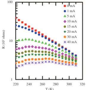
The sample was illuminated by a GaAs infrared LED and the photon flux is linearly dependent on the current through the LED. Thus, for sake of simplicity, we will refer to the illumination intensity by the corresponding current from here on. In Figure 1 we present the electrical resistance R as a function of the temperature for different
illumination intensities. For dark conditions, i.e., with 0 mA, R increases as the temperature decreases while
under illumination it decreases below 240 K when the illumination varies from 0 mA to 10 mA. For illumination with current above 10 mA, the electrical resistance oscillates as the temperature decreases between 260 K and 240 K and starts to decrease for temperatures below 240 K. In Figure 2a we present the normalized R as a function of the
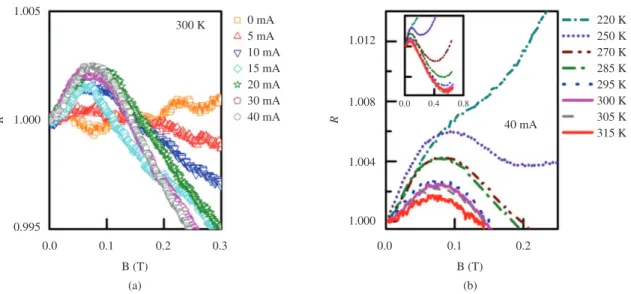
magnetic field with different illumination at T = 300 K.
Through this figure we observe that no magnetoresistive effect is observed in dark conditions (0 mA) (e.g. the slight oscillations have no physical meaning) while a negative magnetoresistance can be observed for illumination with current of 5 mA. For illuminations with current higher
than 5 mA, the curves exhibit positive peaks followed by negative magnetoresistance as the magnetic field increases. In Figure 2b, we show the normalized R as a function of
the magnetic field for different temperature values at a fixed illumination with current of 40 mA. The amplitude of the peaks increases as the temperature decreases in the region for B < 0.2 T while a parabolic behavior is observed for B > 0.4 T due to the classical orbital effect (see inset). In
Figure 2b some curves were omitted in order to simplify the view.
4. Discussion
The electron-hole combination/recombination process via deep level defects is temperature dependent and its rate is different for conduction and valence bands under illumination conditions. The temperature for which R starts
to decrease observed in Figure 1 could be related to the temperature dependence of the combination/recombination rates in the conduction/valence bands. For example, if the hole recombination time increases as the temperature decreases the hole remains longer in the valence band leading to an enhancement of the conductivity in that channel. This also implies that the ratio between electrons and holes is temperature dependent. In fact, n- to p-type
transition is possible for illuminated GaAs samples17. In Table 1 we observe that the carriers mobility obtained when the sample is illuminated is about 0.119 m2/Vs at
T = 300 K. This value is lower than the value found in the
literature for electrons (~0.850 m2/Vs) and higher than the value for holes (~0.04 m2/Vs). Deriving the carriers mobility considering a multi-channel mechanism18, we found that the effective mobility decreases if the ratio p/n increases
and a value of p/n = 102 would lead to the mobility values shown in Table 1. This indicates that holes are the majority carriers in this sample. In addition, using the parameters
Figure 1. Electrical resistance as a function of the temperature for different illumination intensities. The temperature varied from 220 K up to 315 K while the illumination intensity increases with current ranging from 0 mA up to 40 mA.
given in Rubinger et al.19, we calculate the band to impurity recombination time (τR) for electrons and holes taking the AsGa defects concentration about 1025 m–3[20]. We found that the recombination time for holes (τh
R) is about (5-6) × 10 –9 s between 315 K and 220 K while for electrons (τe
R) it is about (5-12) × 10–12 s in the same range of temperature.The elastic scattering time varies from 2.89 × 10⁻¹³ s to 9 × 10–13 s in the range of 315 K to 250 K. Hence, we observe that τh
R, τ6
R >> τ but also that τ h R >> τ
6
R. This analysis also indicates that the holes are the majority carriers for the band conduction processes in the range of temperature analyzed, i.e., the condition τR >> τ indicates that the carrier has time enough to diffuses through the band before recombines back to the impurity level.
The positive magnetoresistance observed on Figure 2a, b in the region of low magnetic fields (B < 0.2 T), can have
different origins. For insulator materials, where the hopping conduction is the main conduction mechanism, the shrinkage of the electronic wave functions caused by the application of a magnetic field could cause such positive magnetoresistance21. In this case, the carrier becomes more localized in a certain space region, increasing
the electrical resistance as the magnetic field increases. However, no positive magnetoresistance is observed under dark conditions according to Figure 2a where the hopping conduction mechanism dominates in this sample. In addition, the magnetic length lB (~10–7 m) is always larger than the mean free path l that is around ~10–8 m, in the range 220-315 K, indicating that the confinement due the magnetic field is negligible.
On the other hand, since the magnetoresistance presented in Figure 2 exists only under illumination, one can suggest that such effect could be caused by the influence of the magnetic field on the electron/hole recombination time. In fact, recombination can be spin-dependent and hence, magnetic field dependent. If the relative spins alignment is destroyed by a magnetic field, the recombination rate (1/τR) increases leading to an increase of the resistivity22. However, a spin-dependent conductivity change of only ∆σ/σ0 ~ 0.1% has been observed at cryogenic temperatures and under the application of an external magnetic field in Si or Ge22,23. The effect of the magnetic field on spin dependent recombination is more pronounced if the sample is illuminated by circularly polarized light24. GaAsN samples illuminated by circularly polarized light can exhibit photo-conductive variations of 40%25. However, such effect has not been observed in undoped GaAs samples25. In addition, only 0.05% of the light applied on our sample was found to be circularly polarized which is not sufficient to cause the magnetoresistance profiles reported here.
The weak antilocalization effect is another physical phenomenon that could give rise to the positive magnetoresistance observed in Figure 2a, b. Weak localization is a quantum effect that arises from the quantum interference between the electronic wave functions moving in the same path but in opposite directions. If the electronic wave functions have the same phase, the interference is constructive leading to a spatial localization of the electrons. This effect can be observed as a negative magnetoresistance
Figure 2. a) Normalized electrical resistance R at 300 K for different illumination intensities. The peaks observed for B < 0.2 T scale with the light intensities which varies with the electrical current through the LED. b) Normalized electrical resistance for different temperatures at 40 mA through the LED. The peaks are also temperature dependent. The inset shows the curves for higher magnetic fields where the classical parabolic behavior of magnetoresistance can be observed.
Table 1. Temperature (T ), carrier mobility (µ), the parameter C, and the hole concentration p.
T(K) µ(m2/Vs) C(×10–14 m2) t
315 0.102 4.30 0.575
305 0.110 4.35 0.539
300 0.119 4.00 0.528
295 0.135 4.80 0.506
290 0.162 5.50 0.455
285 0.173 5.70 0.450
280 0.180 5.40 0.443
270 0.216 5.40 0.434
Antilocalization Effect on Photo-Generated Carriers in Semi-Insulating Gaas Sample
(positive magnetoconductance) if an external magnetic field is applied to the system1. If the spin-orbit coupling in not negligible as compared to other possible interaction mechanism, the interference is destructive and the localization is suppressed leading to the effect called weak antilocalization which can be detected as a positive magnetoresistance (negative magnetoconductance)1. In this case, experimental data can be analyzed using the Fukuyama-Hoshino model and the spin-orbit coupling strength can be obtained15.
Recently, the Fukuyama-Hoshino theory has been successfully applied to GaAs low temperature MBE layers heavily doped with Si and Be where positive and negative magnetoresistance was observed as in our case12. Also, in Jung et al.12, they attributed the localization effects observed at temperatures as high as room temperature to the strongly localized carriers due to the presence of deep level impurities. Under such circumstances the localization effect can be observed since the carrier mean free path is shorter than the phase relaxation length. The difference from the case presented in Jung et al.12 to the present work is that the carriers in the sample studied here are photo-generated instead of excited from shallow donors and acceptors. According to the Fukuyama-Hoshino model, the contribution to the magnetoconductivity due to the localization effects is given by the following equation:
( )
(
)
+ −
− +
∆σ = + + − −
− γ − + − +
− γ
, 1 1
2 1
1
1 1
B T t h t t
hF F F
A h h h
t t t t
(1)
where
2 1 2 2
3
2
e A
C
=
π , 3
Be h= C
, 4 so
i
t=τ
τ
( )
2kh
γ = ,
(
)
1 1 1 2
t±= +t ± − γ
2 /
so
C= τl τ, where l is the mean free path, τ, τi and τso are the elastic, inelastic and spin-orbit scattering times, respectively, F(x) is Kawabata’s function and
(
∗)
∗=3 / /ε τ
8 o F
k m m g .
According to Equation 1, the model also requires that γ < 1. This condition is well satisfied for magnetic fields up to ~0.2 T. As told before, we consider that the holes are the majority carries in the range of 220 K to 315 K. Particularly, the spin-orbit interactions are expected to be stronger in p-type materials and, in fact, this has been
observed over different systems10,26,27. This fact is due to the
p-like symmetry of the states at the top of the valence7. In addition, the p-like symmetry of hole states ensures that they
are weakly coupled to nuclear spins, which could provide long spin coherence times. For the fitting procedure, we use the quantities C, t and k as fitting parameters and plotted the
experimental data presented in Figure 2b as ∆σ in order to compare with the theoretical calculations.
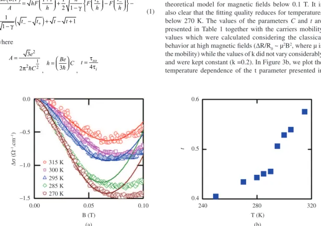
The fitting results are presented in Figure 3a for 0 < B < 0.1 T at the temperatures of 270, 285, 295, 300
and 315 K (the number of curves was reduced in order to clarify the visualization). Through this figure, one observes that the experimental curves are well described by the theoretical model for magnetic fields below 0.1 T. It is also clear that the fitting quality reduces for temperatures below 270 K. The values of the parameters C and t are
presented in Table 1 together with the carriers mobility values which were calculated considering the classical behavior at high magnetic fields (∆R/R0 ~ µ2B2, where µ is the mobility) while the values of k did not vary considerably and were kept constant (k =0.2). In Figure 3b, we plot the temperature dependence of the t parameter presented in
Figure 3. a) Magnetoconductivity correction according to the theoretical model (solid lines) as a function of the temperature together with the experimental points for a GaAs sample with 40 mA through the GaAs LED. The temperature varied from 220 K up to 315 K. For sake of simplicity, some curves were omitted. b) Temperature dependence of the
4 so
i
t=τ
τ parameter presented in Table 1. According to this figure,
t decreases as temperature decreases indicating that spin-orbit coupling becomes more effective than the inelastic scattering mechanism.
5. Conclusions
We have reported on magnetoresistance measurements performed on an illuminated semi-insulating GaAs sample with intrinsic deep level defects. Positive and negative magnetoresistances were observed for B < 0.2 T in the
whole range of temperatures measured (220-315 K). For
T > 240 K we explain the positive magnetoresistance
curves as a manifestation of the weak antilocalization effect which is a consequence of the spin-orbit coupling interaction over the hole carriers. The Fukuyama-Hoshino model gives a good description of the experimental curves according to the antilocalization theory. From the analysis, we estimated the value of the spin-orbit scattering time at room temperature and found that it is close to the values reported before for bulk and GaAs quantum wells.
Acknowledgements
The authors acknowledge the Brazilian Agencies CNPq, CAPES and FAPEMIG for financial support.
Table 1. According to this figure, t decreases as temperature
decreases indicating that spin-orbit coupling becomes more effective than the inelastic scattering mechanism. This is in accordance with the increasing of the positive peaks observed in Figure 2a, b or the corresponding negative magnetoconductance observed in Figure 3a.
It is still possible to estimate the value of τso rewriting
C relation as τso = Cτ / l2. From the carriers mobility one can derive the elastic scattering time, i.e.,τ = mhµ / e, where mh
is the hole effective mass (~0.5 × m0). The mean free path
can be calculated from l = vFτ, where vF=
( )
3π2p1/3/mh isthe Fermi velocity. Considering a parabolic approximation, the values of the carriers concentration p can be derived
substituting the Fermi energy ε =2
( )
π2 2 /3 3 / 2 ,
F p mh in
the k relation above giving = τ
( )
π
3/2 2/3
2 2
3 h2 / 8 3
p m g m k .
Thus, for T = 315 K and using the data presented in Table 1
we estimated τso ~ 4.9 × 10⁻¹¹ s.
This value agrees with the already reported results for Bulk GaAs samples at room temperature28 and for those obtained for GaAs quantum wells at low temperatures8.
References
1. Bergmann G. Weak Localization in Thin Films.
Physics Reports. 1984; 107(1):1-58. http://dx.doi.
org/10.1016/0370-1573(84)90103-0
2. Lin BJF, Paalanen MA, Gossard AC and Tsui DC. Weak localization of two-dimensional electrons in GaAs-AlGa1-As heterostructures. Physical Review B. 1984; 29:927-934. http://
dx.doi.org/10.1103/PhysRevB.29.927
3. Lin JJ and Bird JP. Recent experimental studies of electron dephasing in metal and semiconductor mesoscopic structures.
Journal of Physics: Condensed Matter. 2002; 14(18):R501.
http://dx.doi.org/10.1088/0953-8984/14/18/201
4. Altshuler BL, Aronov AG and Lee PA. Interaction effects in disordered fermi systems in two dimensions. Physical Review Letters. 1980; 44:1288-1291. http://dx.doi.org/10.1103/ PhysRevLett.44.1288
5. Anderson PW, Abrahms E and Ramakrishnan TV. Possible explanation of nonlinear conductivity in thin-film metal wires.
Physical Review Letters. 1979; 43:718-720. http://dx.doi. org/10.1103/PhysRevLett.43.718
6. Gilbertson AM, Newaz AKM, Chang W-J, Bashir R, Solin SA and Cohen LF. Dimensional crossover and weak localization in a 90 nm n-GaAs thin films. Applied Physics Letters. 2009; 95:012113-6. PMid:19668705 PMCid:2723832.
http://dx.doi.org/10.1063/1.3176968
7. Grbic B, Leturcq R, Ihn T, Ensslin K, Reuter D and Wieck AD. Strong spin-orbit intereactions in carbon doped p-type GaAs heterostructures. Physica E. 2008; 40:2144-2146. http://dx.doi.
org/10.1016/j.physe.2007.10.037
8. Desrat W, Maude DK, Wasilewski ZR, Airey R and Hill G. Dresselhaus spin-orbit coupling in a symetric (100) GaAs quantum well. Physical Review B. 2006; 74:193317-21. http://
dx.doi.org/10.1103/PhysRevB.74.193317
9. Cabañas S, Schapers TH, Thillosen N, Kaluza N, Guzenko VA and Hardtdegen H. Suppression of weak antilicalization in an AlxGa1-xN/GaN two-dimensional electron gas by an in-plane magnetic field. Physical Review B. 2007; 75:195329-34. http:// dx.doi.org/10.1103/PhysRevB.75.195329
10. Papadakis SJ, De Poortere EP, Manoharan HC, Yau JB, Shayegan M and Lyon SA. Low-field magnetoresistance in GaAs two-dimensional holes. Physical Review B. 2002; 65:245312-9. http://dx.doi.org/10.1103/PhysRevB.65.245312
11. Look DC. Molecular beam epitaxial GaAs grown at low temperatures. Thin Solid Films. 1993; 231:61-73. http://dx.doi.
org/10.1016/0040-6090(93)90703-R
12. Jung DW, Noh JP, Islam AZMT and Otsuka N. Enhanced electron-electron interaction in GaAs layers doped with high concentrations of donor and acceptor impurities. Journal of the Physical Society of Japan. 2008; 77:074721-8. http://dx.doi. org/10.1143/JPSJ.77.074721
13. Lin TC and Okumura T. Characterization of annealed low-temperature GaAs layers grown by molecular beam epitaxy with n-i-n structure. Japanese Journal of Applied Physics. 1996; 35:1630-1636. http://dx.doi.org/10.1143/
JJAP.35.1630
14. Jost W, Kunzer M, Kaufmann U, Kohler K, Schneider J and Alt HC. AsGa antisite defects in LT GaAs as studied by magnetic resonance and magneto-optical techniques. Semiconductor Science and Technology. 1992; 7:1386-1389. http://dx.doi.
org/10.1088/0268-1242/7/11/017
15. Fukuyama H and Hoshino K. Effecto of spin-orbit interaction on magnetoresistance in the weakly localized regime of three-dimensional disordered systems. Journal of the Physical Society of Japan. 1981; 50:2131-2132. http://dx.doi.
org/10.1143/JPSJ.50.2131
16. Datta S and Das B. Electronic analog of the electro-opitc modulator. Applied Physics Letters. 1990; 56:665-667. http://
dx.doi.org/10.1063/1.102730
17. Da Silva MIN, De Oliveira AG, Ribeiro GM, Rubinger RM, Corrêa JA and Baeta MMV. EL2-like metastable defect and the n- to p-type transition in silicon planar-doped GaAs. Journal of Applied Physics. 1997; 82:3346-3350. http://dx.doi. org/10.1063/1.365645
Antilocalization Effect on Photo-Generated Carriers in Semi-Insulating Gaas Sample
24. Kalevich VK, Shiryaev AYu, Ivchenko EL, Afanasiev MM, Egorov AYu, Ustinov VM et al. Hanle effect and spin-dependent recombination at deep centers in GaAsN.
Physica B. 2009; 404:4929-4932. http://dx.doi.org/10.1016/j. physb.2009.08.234
25. Zhao F, Balocchi A, Kunold A, Carrey J, Carre H, Amand T et al. Spin-dependent photoconductivity in nonmagnetic semiconductors at room temperature. Applied Physics Letters. 2009; 95:241104. http://dx.doi.org/10.1063/1.3273393 26. Peres ML, Chitta VA, Oliveira Junior NF, Maude DK,
Rappl PHO, Ueta AY et al. Antilocalization of hole carriers in Pb1-xEuxTe alloys in the metallic regime. Physical Review B. 2009; 79:085309-12. http://dx.doi.org/10.1103/ PhysRevB.79.085309
27. Grbic B, Ellenberger C, Ihn T, Ensslin K, Reuter D and Wieck AD. Magnetotransport in C-doped AlGaAs heterostructures.
Applied Physics Letters. 2004; 85:2277-2279. http://dx.doi. org/10.1063/1.1781750
28. Spezia S, Adorno D P, Pizzolato N and Spagnolo B. Relaxation of electron spin during high-field transport in GaAs bulk.
Journal of Statistical Mechanics. 2010; 11033. http://dx.doi.
org/10.1088/1742-5468/2010/11/P11033 equilibrium Hall concentration in silicon planar-doped GaAs
samples. Solid State Communications. 1996; 98:1063-1068. http://dx.doi.org/10.1016/0038-1098(96)00146-9
19. Rubinger RM, Bezerra JC, Chagas EF, González JC, Rodrigues WN, Ribeiro GM et al. Thermally stimulated current spectroscopy on silicon planar-doped GaAs samples.
Journal of Applied Physics. 1998; 84:3764-3769. http://dx.doi. org/10.1063/1.368588
20. Krambrock K, Linde M, Spaeth JM, Look DC, Bliss D and Walukiewicz W. Arsenic antisite-related defects in low-temperature MBE grown GaAs. Semiconductor Science and Technology. 1992; 7:1037-1041. http://dx.doi.
org/10.1088/0268-1242/7/8/002
21. Shklowskii BI and Efros AL. Electronic properties of Doped Semiconductors. Springer-Verlag Berlin; 1984. v. 45, 210
p. Springer Series of Solid State Science.
22. Lepine DJ. Spin-Dependent Recombination on Silicon Surface.
Physical Review B. 1972; 6:436-441. http://dx.doi.org/10.1103/
PhysRevB.6.436
23. Dersch H, Schweitzer L and Stuke J. Recombination process in a-Si:H: Spin-dependent photoconductivity. Physical Review B. 1983; 28:4678-4684. http://dx.doi.org/10.1103/
PhysRevB.28.4678