1
Enhanced UV flexible photodetectors and
photocatalysts based on TiO
2
nanoplatforms
D. Nunes1,*, A. Pimentel1, A. Araujo1, T.R. Calmeiro1, S. Panigrahi1, J.V. Pinto1, P. Barquinha1, M. Gama2, E. Fortunato1,* and R. Martins1,*
1i3N/CENIMAT, Department of Materials Science, Faculty of Sciences and Technology, Universidade NOVA de Lisboa and CEMOP/UNINOVA, Campus de Caparica 2829-516, Caparica
2Centre of Biological Engineering – CEB, University of Minho, Campus de Gualtar, 4710-057, Braga, Portugal
Abstract
In this study, titanium dioxide (TiO2) nanostructured films were synthesized under
microwave irradiation through low temperature synthesis (80 ºC) and integrated in ultraviolet (UV) photodetectors and as photocatalysts. Bacterial nanocellulose (BNC), tracing paper, and polyester film were tested as substrates, since they are inexpensive, flexible, recyclable, lightweight, and when associated to low temperature synthesis and absence of seed layer, they become suitable for several low-cost applications. The nanostructured TiO2 films and substrates were structurally characterized by scanning
electron microscopy (SEM) coupled with energy dispersive X-ray spectroscopy (EDS), X-ray diffraction (XRD), and Raman spectroscopy. The optical properties of all materials were investigated. The TiO2 nanostructured films were implemented as a photoactive
layer of UV photodetectors and demonstrated significant increase of conductance upon exposed to UV irradiation. The photodetection behaviour of each material was investigated by in-situ Kelvin probe force microscopy (KPFM) experiments, in which the contact potential difference varied under dark or UV irradiation conditions, demonstrating higher shift for the BNC-based UV photodetector. Photocatalytic activity of the films was assessed from rhodamine B degradation under solar radiation, and BNC based devices revealed to be the best photocatalyst. The structural characteristics of the TiO2 films and substrates were correlated to the differences in the UV photodetection and
photocatalytic performances.
Keynotes: TiO2 nanostructured films; flexible substrates; microwave irradiation; UV
photodetectors; low-cost devices.
*i3N/CENIMAT, Department of Materials Science, Faculty of Sciences and Technology, Universidade NOVA de Lisboa and CEMOP/UNINOVA, Campus de Caparica 2829-516, Caparica; Correspondence should be addressed to: [email protected] (D. Nunes), [email protected] (E. Fortunato) and [email protected] (R. Martins), +351 212948558 and +351 212948562 (fax and telephone, respectively).
2
Introduction
Titanium dioxide (TiO2) is an extremely versatile material as it can be employed
in numerous applications, such as self-cleaning surfaces [1], dye sensitized solar cells [2-4], photocatalysis [5,6], and photosensors/photodetectors [7,8]. The interest on the latter application has been increasing with special attention to UV photodetectors. These are of great interest for everyday life especially in terms of sun/UV exposure, as well as for industry with direct applications in environmental safety, flame detection, among others [9]. The most common UV photodetectors used nowadays are the silicon-based ones, however this sort of devices present limitations, mostly associated to their narrow band gap energy (1.1 eV), and high temperature processing [9]. TiO2-based photodetectors are
excellent alternatives asTiO2 is highly photoactive and stable under UV irradiation due
to its band gap [10,11], 3.00 and 3.21 eV for rutile and anatase, respectively [12]. Regarding brookite’s band gap, the values reported in literature are diverse, ranging from 3.13 to 3.40 eV [12,13]. Moreover, TiO2 is a highly stable material, earth-abundant,
low-cost, non-toxic [5], and it is largely employed as photocatalyst, normally in the anatase and rutile phases, or as mixtures of both phases to increase photocatalytic activity. Brookite, on the other hand is less explored, however its photocatalytic interest has been growing lately [6,14].
The TiO2 photoconductivity relies on the electrical conductivity changes under
irradiation. The photodetection is governed by a hole-trapping mechanism based on the adsorption/desorption of chemisorbed oxygen molecules at the surface [15]. An analogous mechanism occurs in photocatalysis, where electron–hole pairs are generated. These photogenerated holes and electrons diffuse to the surface, oxidizing and reducing oxygen and water molecules, and creating reactive radicals that will decompose organic and inorganic compounds on the surface of TiO2 [6,16]. Kelvin probe force microscopy
can be used to map the electronic properties of photoactive materials, measuring the contact potential difference (CPD) shift [17] (CPD with and without irradiation) and the surface potential, thus allowing the correlation with the photosensitivity of the materials [18]. This allows to understand the photosensitivity behaviour of sensing materials. The high sensitivity and stability of the photodetector associated to inexpensive materials and synthesis routes are imperative for obtaining low-cost and efficient devices.
Polymer and biopolymer materials fully fulfil the requirements for producing economically viable and flexible devices, hence the rapid and growing interest concerning
3
the use of these materials as substrates for advanced devices being a reality nowadays. Cellulose is the most abundant biopolymer on earth [19,20]. Bacterial nanocellulose (BNC) and tracing paper are valuable materials for the development of disposable and inexpensive devices. BNC displays several advantages over other types of cellulose, in which the main one is the enhanced chemical purity, low surface roughness and porosity. Moreover, BNC displays high crystallinity, a finer and intricate structure, with longer and stronger fiber lengths. The bacteria Gluconacetobacter is normally responsible for the production of BNC membranes in large amounts, becoming an alternative for plant cellulose and thus preserving the environment [21]. Polymer substrates, i.e. polyester films, are also alternative substrates for the development of photodetectors, since they can easily and flexibly adapt to surfaces, are lightweight and impermeable, despite the possibility of recycling plastic waste.
The fabrication route plays a central role on the final cost of the device. Several techniques have been reported to produce TiO2 nanostructures/films, which included
thermal evaporation [22], sputtering [23], hydrothermal or solvothermal synthesis [24,25], and microwave synthesis [5,6], and even with waste reuse [26]. Nevertheless, microwave synthesis appears as an attractive option, since it is a simple and fast technique, low-priced, with intrinsic properties that can easily adapt to soft substrates and low temperature synthesis [6]. The efficient heating of solvents and/or reagents [27,28] is guaranteed, providing accurate temperature control, and assuring homogeneity and uniformity of the produced materials. Moreover, for most of these synthesis routes, a seed layer is usually required. Indeed, the seed layer facilitates nucleation and determines the perfect covering of substrates, together with the crystallization, phase formation, and surface morphology of the growing film [29]. However, the deposition of a seed layer adds to the device extra procedures and in some cases requiring an additional annealing treatment, thus representing an additional cost.
The present work reports the production and characterization of TiO2
nanostructured films grown on BNC, paper and polyester substrates, under microwave irradiation at low temperature (80 ºC) and without any seed layer. The aim is to challenge the present state of the art concerning the exploitation of enhanced TiO2 photoactive
layers produced with low-cost synthesis routes in different substrates but also the fabrication of highly efficient but simple, environmentally friendly, low-cost and disposable UV photodetectors and photocatalysts. Moreover, to the best of the authors’ knowledge, TiO2 films grown under microwave irradiation without any seed layer at low
4
temperature with cellulose- and polymer-based substrates to be employed as UV photodetectors and photocatalysts has never been reported before. Structural characterization of the TiO2 films has been carried out by scanning electron microscopy
coupled with an EDS detector, Raman spectroscopy, and X-ray diffraction. The optical characterization has been also carried out for all materials. In-situ Kelvin probe force microscopy experiments were carried out under UV irradiation.
Experimental procedure
TiO2 film synthesis
The TiO2 nanostructured films have been synthesized under microwave irradiation.
The TiO2 microwave solution has been prepared using titanium (IV) isopropoxide
(Ti[OCH(CH3)2]4, TTIP, 97% from Sigma Aldrich), hydrochloric acid (HCl, 37%) and
deionised water. In a typical synthesis, 50 mL of water was mixed with 10 mL of HCl and stirred for 5 min. Afterwards, 2 mL of TTIP was added and the final mixture stirred for 10 min before microwave synthesis. Microwave synthesis was performed using a CEM Focused Microwave Synthesis System Discover SP. Time, power, temperature and pressure were set at 60 min, 100 W, 80 ºC and 17 bar, respectively. The selected proportions of all reagents and synthesis parameters were determined following an analogous study [6] and intending to keep synthesis temperature, power input and acid amount to the minimum to guarantee the TiO2 nanostructured film formation, and at the
same time preventing any damage to the substrates. Solution volumes of 20 mL were transferred into capped quartz vessels of 35 mL, which were kept sealed by the constraining surrounding pressure.
Three types of flexible substrates were used, i.e. bacterial nanocellulose, tracing paper and polyester film. The BNC was synthesized by the bacteria Gluconoacetobacter
xylinum in the form of a wet membrane [30]. The nanocellulose is excreted into the
aqueous culture medium directly as nanofibers, with a diameter ranging from 25 – 100 nm [31]. This membrane was produced as described elsewhere [32] and then oven dried, forming a membrane with some tens of micrometers. The tracing paper is from Canson with 90 g/cm2, translucent and perfectly flat [33]. The polyester substrate has its
commercial name as Mylar film and has been purchased from DuPont with one side chemically pre-treated for better adhesion. The polyester substrate was used as-purchased, and no other treatment has been carried out. During microwave synthesis, a
5
piece of each substrate (20.0 20.0 mm) was placed at an angle against the vessel and in the case of the polyester, the chemically treated side was facing down [5].
TiO2 film characterization
X-ray diffraction experiments were performed using a PANalytical's X'Pert PRO MPD diffractometer equipped with a X’Celerator 1D detector and using CuK radiation. The XRD data were acquired in the 20 - 60o 2 range with a step size of 0.05 º.For
comparison, powder diffractograms of rutile, anatase, brookite have been simulated with PowderCell [34] using crystallographic data from reference [35].
Micro-Raman spectroscopy experiments were carried out with a Labram 300 Jobin Yvon spectrometer, equipped with a 17 mW He–Ne laser operating at 532 nm. Surface and cross-section SEM observations were carried out using a Carl Zeiss AURIGA CrossBeam FIB-SEM workstation equipped for EDS measurements. The dimensions of individual nanorods and films have been determined from SEM micrographs using the ImageJ software [36].
Surface potential mapping was measured using the Kelvin probe force microscopy technique in air at room temperature with an MFP-3D Standalone Asylum Research instrument in tapping mode. Olympus AC240 TM platinum coated silicon probes with a natural resonance frequency (f0) of ~70 kHz and a nominal spring constant (k) of ~2 N/m
have been used. The scanning ranges were 2 2 and 5 5 m2 with a resolution of at
least 256 by 256 lines in all acquisition channels. The KPFM experiments were carried out in a double pass mode, and the second pass was performed at an optimized height of 50 nm above the topographic trace [37]. During UV irradiation, the materials were illuminated with UV (λ = 365 nm) [38] collimated LEDs from Thorlabs. The root mean square (RMS) roughness of each substrate was obtained from atomic force microscopy (AFM) topography images.
Room temperature reflectance measurements were performed in the 250 – 800 nm range with a PerkinElmer lambda 950 UV/VIS/NIR spectrophotometer equipped with a 150 mm diameter integrating sphere. The calibration of the system was achieved by using a standard reflector sample (reflectance, R = 1.00 from Spectralon disk). The band gap of the TiO2 films was estimated from reflectance spectra using the Tauc plot method
[39-41].
The pristine substrates were also characterized through XRD, SEM and Raman spectroscopy for understanding their influence on the TiO2 films produced.
6 TiO2 UV photodetectors production and characterization
The TiO2 nanostructured films grown on all flexible substrates were tested as
photoactive layers on UV photodetectors. For the assembly of the complete device, a shadow mask was used for patterning interdigitated contacts [42] and an Au/Pd film of 100 nm was then sputtered at room temperature (Figure 1). The Au/Pd interdigitated contacts were selected since a Schottky interface is expected to be formed between metals with large work function (such as Pd and Au) and n-type TiO2 [43]. The formed junction
has a rectifying electrical transport behaviour, resulting in efficient charge separation of the photogenerated electron–hole pairs, and thus preventing the electron–hole recombination [43].
The devices characterization has been carried out using a potentiostat model 600 from Gamry Instruments, Inc. in a chronoamperometry configuration, with a constant applied voltage of 10 V. The photodetectors were subjected to UV irradiation using two ultraviolet lamps, model TK-2028 from Hongguang Optics International Industry Co. Ltd., with 6 W (each) at a wavelength of 360 nm. The produced photodetectors were irradiated for 15 min followed by 30 min in off state. The I–V characteristics of the flexible photodetectors were measured by sweeping the voltage from -5 V to 5 V with a step of 10 mV s-1.
Figure 1 – Scheme of the TiO2 UV photodetector production stages and photograph of the final device
showing high flexibility.
Photocatalytic activity
The photocatalytic activity of the TiO2 nanostructured films was evaluated at
room temperature from the degradation of rhodamine B from Sigma Aldrich under a solar light simulating source. The experiments were not carried out with the direct exposure to sunlight. The experiments considered the International standard ISO 10678. The TiO2
films were placed on the bottom of the reaction recipient and for each experiment, 50 ml of the rhodamine B solution (5 mg/L) was stirred for 30 min in the dark to establish
7
absorption–desorption equilibrium. The photocatalytic activity experiments used a Xe lamp at room temperature with intensity of 100 mW cm2 and AM1.5 spectrum [6].
Absorption spectra were recorded using a PerkinElmer lambda 950 UV/VIS/NIR spectrophotometer with intervals of 60 min for the first 8 hours, and after with intervals of 120 min up to 12 hours, then a 180 min exposure was carried out to complete a total exposure time of 15 hours. To perform reusability experiments, the material was dried after the first exposure, at 50 ºC for 1 h, and the liquid was discarded. The reusability tests were carried out by the repeated solar radiation exposure of the same sample in fresh solutions for different intervals of time up to15 h.
Results and discussion
TiO2 nanostructured films were successfully synthesized under microwave irradiation
using cellulose- and polymer-based substrates at low temperatures and without any seed layer. The distinct substrates were selected due to their specific characteristics, i.e. BNC is transparent and together with tracing paper, both have lack of porosity when compared to other types of papers, making them suitable for optoelectronic devices. The polymer-based material is highly flexible and resistant being also largely integrated in such devices. The TiO2 films, substrates and final devices were systematically investigated
including their behavior under UV irradiation and dark conditions.
Structural characterization
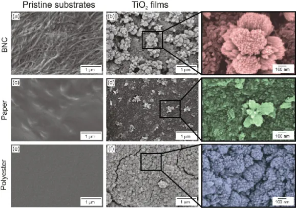
Figure 2 shows the SEM images of TiO2 nanostructured films presented together with
the pristine substrates for comparison. A clear difference is observed between the substrates before and after microwave irradiation. The pristine BNC substrate appears with a well-organized 3D structure, forming a closed packed cellulose nanofiber network with irregular interconnected pores (Figure 2 (a)). AFM measurements revealed a RMS roughness value of 58 nm (see supplementary information Figure S1). The tracing paper and polyester substrates are more compact materials without any defined structures (Figures 2 (c) and (e)), despite the higher roughness of tracing paper. In fact, AFM showed that tracing paper displayed a rougher surface with a RMS value of 312 nm (Figure S1). The polyester film has a chemically pre-treated surface, however no particular pattern/roughness could be discerned by SEM. AFM measurements revealed a RMS roughness value of 11 nm (Figure S1).
8
Microwave irradiation resulted in uniformly covered substrates, forming continuous TiO2 films with two distinct film characteristics. Individual nanostructured particles with
an undefined structure (ranging from small sized squares to rod-like structures) covered mostly of the cellulosed-based substrates and fine nanorod aggregates forming TiO2
flower-like structures were also observed (higher extent on the BNC material when compared to the paper substrate). After microwave synthesis, the nanofiber network can still be noticed on the BNC-based material, however completely covered with the TiO2
film (see Figure S2 (a)). On the polyester substrate, these flower-like structures were grown side-by-side appearing as a continuous material formed by densely and closely packed nanorod aggregates. Nevertheless, some cracks along the film could be observed (Figure 2 (f)). In all materials, the average nanorod widths were similar with 11 ± 3 nm (magnified SEM image of the nanorods is presented in Figure S2 (b)). These fine aggregated nanorods have been reported previously [5,44]. These reports suggest that the fine nanorods have the rutile phase and a [001] growth direction [5,44], moreover they tend to combine and thus reduce the surface energy [45] forming the aggregates. This undefined nanostructures has also been previously reported in an analogous work and identified as having the brookite phase [6].
EDS analyses were carried out in the material cross-sections and revealed that the TiO2 film was grown on both sides of the cellulose-based substrates, while for the
polyester material, just the chemically pre-treated side formed a continuous film (Figure 3). Some residual traces of TiO2 could be observed on the untreated side, however, no
continuous film could be observed. The chemically treated surface of the polyester substrate is expected to facilitate the fixation of the film during synthesis. The TiO2
growth on cellulose-based substrates without any seed layer or chemical treatment for adhesion are expected to be due to substrate roughness facilitating nucleation and fixation of the TiO2 structures. Other metal-oxide based materials have been shown to grow on
cellulose-based substrates, however, a seed layer was required for this process to occur [46-48]. The thickness of the films grown on BNC and tracing paper could not be inferred precisely due to heterogeneities of the structures formed, while the TiO2 nanorod film
grown on the polyester substrate revealed a thickness average of 167 ± 9 nm (see Figure 3 (i)). The substrate thickness differences are evident, corresponding to 15 ± 1 m (BNC), 62 ± 9 m (tracing paper) and 21 ± 1 m (polyester).
9
Figure 2. SEM images showing the BNC (a), paper (c) and polyester (e) pristine substrates together with
the TiO2 films grown on BNC (b), tracing paper (d) and polyester (f) substrates. The false colored insets show
the TiO2 films and the nanorod flower-like structures with a higher magnification.
Figure 3. SEM images of the TiO2 films grown on BNC (a), tracing paper (e) and polyester (i) substrates
together with their corresponding EDS maps of C (b, f and j), O (c, g and k) and Ti (d, h and l). The insets show the cross-section SEM images of all materials.
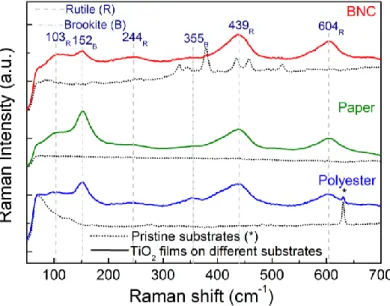
Raman spectroscopy and X-Ray diffraction measurements were carried out for the TiO2 nanostructured films together with their pristine substrates. A substantial
10
contribution from the substrates was observed on XRD diffractograms, hindering the TiO2 signal (Figure S3). Raman spectroscopy was able to overcome this difficulty,
allowing the precise identification of the TiO2 phases present [49] (Figure 4). The pristine
substrate Raman spectra are presented for comparison.
The Raman spectra showed the presence of both brookite and rutile phases for all materials. The Raman bands associated to brookite were detected from 100 to 400 cm-1,
which can be assigned to A1g (152 cm-1) and B2g (355 cm-1) [49]. The Raman bands
associated to rutile can be assigned to B1g (103 cm-1), Eg (244 and 439 cm-1) and A1g (604
cm-1). The characteristic Raman band of ~518 cm-1 [49] associated to the presence of
anatase was not detected in any material. No additional bands could be found in the spectra. In the TiO2 films grown on polyester, the substrate peaks (*) are more intense,
unlike in the case of the cellulose-based ones (such as in XRD results), an effect that might be related to differences in thickness between the TiO2 films (which could not be
estimated for the cellulose-based materials).
Figure 4. Raman spectra of the TiO2 films together with their pristine substrates (dot lines). Dashed lines
indicate the rutile bands and dot/dashed ones point out to the brookite ones.
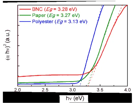
Optical characterization
Optical band gaps have been evaluated from reflectance data through the Tauc plot. The optical band gap is related to the optical absorption coefficient and the incident photon energy as follows [40,50]:
𝛼ℎ𝑣 = 𝐴(ℎ𝑣 − 𝐸g) 𝑛
11
where α is the linear absorption coefficient of the material, hν is the photon energy, A is a proportionality constant and n is a constant exponent which determines the type of optical transitions (n = 1
2
⁄ for direct allowed transition and n = 2 for indirect ones).
Moreover, for determining the band gap, the (αhν)2 against hν is plotted, and extracted
through the intersection of the extrapolation of the linear portion with 0. The band gaps were estimated to be 3.28 eV, 3.27 eV, and 3.12 eV for the TiO2 films grown on BNC,
tracing paper and polyester substrates, respectively (Figure 5). The evaluated band gaps are within the reported values for the different TiO2 phases [51,52,12], i.e. for the rutile
phase (3.00 eV) and brookite (3.13-3.4 eV) [12,13]. The band gap is strongly dependent on crystallite size [53,54], phase present [5], defects [42], residual strain [55], degree of compactness and densification [56], among other factors. No significant band gap differences were observed between the cellulose-based materials, while the band gap value of the TiO2 film grown on polyester substrate revealed to be slightly lower. This
difference can be justified by the structural properties of the polyester-based TiO2 films,
such as film thickness [55] and compactness [5].
Figure 5. (hν)2 variation versus photon energy hν for the TiO
2 films grown on BNC, tracing paper and
polyester substrates.
TiO2 UV photodetectors
TiO2 UV photodetectors have been studied over the years, especially the ones based
on nanomaterials, due to their large surface-to-volume ratios assuring high responsivity [57]. The TiO2 phase present on the device also plays a key role on its final behaviour. It
12 [10], thus this drawback can be overpassed with mixtures of TiO2 phases [10]. TiO2 UV
sensing devices based on mixtures of anatase and rutile have been reported [10,58], nevertheless devices based on brookite/rutile phases are rare, and to our best knowledge brookite/rutile UV photodetectors have never been reported, particularly producing flexible devices based on cellulose or polymer substrates. The relatively low stability of brookite can be responsible for this lack of investigation. In fact, brookite can be converted to rutile by a proper thermal treatment [13]. Yet, the combination of both rutile and brookite is expected to produce devices with high performance as both phases have wide band gaps and are excellent UV absorbers [10,13].
The sensitivity of a UV photodetector is also governed by other factors besides the ones already mentioned, i.e. shape, reduced grain size and phase present. Thus, substrate morphology, surface state, oxygen adsorption quantity, oxygen adsorption active energy, lattice defects, and connectivity between grains also contribute to the final device performance [42,59].
The TiO2 films grown on BNC, tracing paper and polyester substrates were tested
as UV photodetectors, and the results are presented in Figure 6. Nevertheless, the heterogeneous structure observed at each material reverberated to their photosensitivity and final UV photodetector behaviour. The time resolved photocurrent of TiO2 films was
measured at room temperature in response to the on/off switching of UV irradiation (Figure 6 (a)). Despite the heterogeneity, the behaviour observed for several UV photodetectors produced with all the substrates was consistent, with the TiO2 film grown
on bacterial nanocellulose displaying enhanced photosensitivity when compared to the other substrates. Under the bias voltage of 10 V, the photocurrent exponentially increased from 0.15 μA (dark condition) to 3.78 μA (UV irradiation) for the TiO2 film grown on
BNC substrate, while for the tracing paper one, it increased from 0.06 μA to 1.99 μA and polyester substrate from 0.01 μA to 0.83 μA. When the UV irradiation was turned off, the current decreased to its initial current value. Moreover, the photocurrent could be reproducibly switched from on to off states several times maintaining the characteristics over time indicating the enhanced stability of all the UV photodetectors. Figure 6 (b) shows the typical current versus voltage (I–V) curves of the TiO2 film UV photodetectors
in the dark and under UV irradiation measured at a bias voltage ranging from -5 to 5 V and at room temperature.The I–V curves revealed an Ohmic contact between the Au/Pd electrodes and the TiO2 films. Upon UV irradiation, and as exhibited on Figure 6 (a), the
13
difference between measurements with UV irradiation and dark condition are evident (see inset in Figure 6 (b)).
The sensing process of the TiO2 photodetectors can be explained as follows:
• On dark conditions, the oxygen molecules adsorbed on the TiO2 surface capture
the free electrons present in the n-type semiconductor, forming a low conductivity depletion layer near the surface [O2(g) + e- → O2- (ads)] (Figure 6 (c)).
• Under UV irradiation at a photon energy above its Eg,electron-hole pairs are photogenerated, and the holes migrate to the surface along the potential slope. This potential slope is produced by band bending and discharge of negatively charged adsorbed oxygen ions through surface electron-hole recombination, leading to oxygen photo desorption [42,60] [h+ + O
2-(ads) → O2(g)] (Figure 6 (c)).
This hole-trapping mechanism through oxygen adsorption and desorption enhances the high density of trap states due to the dangling bonds at the surface and thus enhances the photoresponse [61].
The TiO2 UV photodetector responsivities were also estimated according to the
Equation (2) [42]:
𝑅 = 𝐼𝑝ℎ−𝐼𝑑𝑎𝑟𝑘
𝑃𝑈𝑉 (2)
where Iph is the UV device photocurrent, Idark is the dark current, and PUV is the UV light power. The calculated responsivity was 0.33 A/W, 0.16 A/W and 0.07 A/W for the TiO2 films grown on BNC, tracing paper and polyester substrates, respectively. The
responsivity was calculated taking into account the current value when the device reaches 95% of its stable value [33,62]. Thus, the TiO2 film grown on BNC substrate displayed
the highest responsivity among the other substrates used.
As previously mentioned, several parameters dictate the UV photodetector responsivity. For the present case, no clear relation between the band gaps and the responsivity can be established for all materials, as no significant differences were detected. No significant TiO2 phase differences are expected between all the materials,
however BNC revealed enhanced performance. Thus, no direct input resultant from the TiO2 phases at each material could be directly inferred. Nevertheless, the present study
demonstrated that TiO2 UV photodetectors based on mixtures of brookite/rutile can be
effectively produced with enhanced performance (Figure 6 (a)). Some contribution can be expected from lattice defects, such as oxygen vacancies, which are believed to contribute to the enhanced photosensitivity of materials [61].
14
The observed UV photodetector performances were then justified regarding the structural properties of the TiO2 nanostructured films and their substrates. In fact, films
with different structural characteristics, such as crystal structure, particle size and film thickness, could significantly influence the transport and recombination properties of the photogenerated carriers and thus the UV photodetector performance [63]. In the present case, no direct conclusions could be determined from the TiO2 film thicknesses, since the
thickness could not be estimated, due to heterogeneities of the cellulose-based materials. Nevertheless, a considerable contribution for UV photodetection can be expected due to film thickness [63,64]. Moreover, the nanorods observed in all materials displayed similar widths, thus this parameter seems not to be responsible for the differences in photosensitivity observed.
Regarding the substrate morphology input, clear structural differences between the substrates studied were observed by SEM and AFM measurements (see Figure 2 and S1). In the case of BNC-based materials, significant contribution can be suggested from the substrate structure, as nanocellulose displays high surface-to-volume ratio [65]. The enhanced BNC surface-to volume property can tune the TiO2 nanostructured film features
and thus its sensing behaviour. In fact, this could be observed with the nanofibers covered with the TiO2 film after microwave synthesis (Figure S2 (a)). Moreover, BNC is a closed
packed cellulose nanofiber network with the lowest RMS roughness value among the cellulose-based materials studied. This intrinsic surface characteristic guarantees the growth of continuous nanostructured films without any abrupt gap among the structures formed, which would lead to current loss. The higher roughness of tracing paper, on the other hand, can contribute to discontinuities in the nanostructured film, which decrease the photodetector performance. Regarding the polyester-based materials, the cracks observed along the film can be responsible for the poorest behaviour among the materials tested. In Ref. [33], a wrinkled material after microwave synthesis was assumed to difficult current flow through the sample, decreasing its performance.
15
Figure 6. (a) Cycling behaviour of TiO2 film photodetectors at 10 V and under a 360 nm UV source. (b) I– V curves showing the dark current and photocurrent of the produced devices. (c) Schematic diagrams of
dark and UV irradiation processes. The top drawing shows the schematic of the energy band diagrams, where VB and CB are the valence and conduction band, respectively. The bottom drawing shows the dark and UV irradiation mechanisms, where in dark, the oxygen molecules adsorbed at the surface capture the free electron present in the n-type semiconductor forming a low-conductivity depletion layer near the surface. Under UV irradiation, photogenerated holes migrate to the surface and are trapped, leaving behind unpaired electrons that contribute to the photocurrent [60,61].
Kelvin probe force microscopy
Kelvin probe force microscopy is a powerful technique capable of determining electronic properties of materials at the nanometer scale, such as contact potential differences (CPD) [37]. The CPD (or VCPD) can be related to the material surface potential, through the following equation [60,66]:
𝑉𝐶𝑃𝐷 =(𝜑𝑝−𝜑𝑠)
16
where 𝜑𝑝 and 𝜑𝑠 are the work functions of probe and sample, respectively, and e is the electronic charge. For a semiconductor, it is defined 𝜑 as the surface potential [60]. In general, the local surface potential is due to the charge density on the material surface, depending on the presence of charges on the surface but also beneath it, surface dipoles, and polarization effects [67].
Figures 7 and S4 show the CPD averaged profiles together with the corresponding topography and surface potential images carried out in air and with/without UV irradiation of the TiO2 films grown on BNC, tracing paper and polyester substrates. The
CPD of all TiO2 films increased with the UV irradiation. Nevertheless, from the CPD
averaged profiles, the shift under UV irradiation is not linear and changed regarding the material tested.
The film surface potential, which is related to CPD, depends on its own characteristics such as thickness; however, some contribution also comes from the substrate [67] below the film. In the present case, the substrates are completely distinct, with different surfaces, roughness and thicknesses, leading to different surface potential contributions. This behaviour has been previously reported with different substrates, leading to distinct surface potentials of the deposited films [67]. For that reason, the averaged CPD measured cannot be linearly comparable between the materials, but instead its shift detected with and without UV irradiation. Moreover, considering Equation (3) and using the same calibrated probe during UV on/off measurements, it can be assumed that the CPD shift is equal to the surface potential shift.
Several KPFM measurements in distinct TiO2 photodetectors were performed and
the results are presented in Figures 7 and S4. In Figure 7, the averaged CPD for the TiO2
film grown on BNC substrate increased from 420 mV in dark to 530 mV under UV, while the film grown on tracing paper increased from 280 to 320 mV, dark and UV, respectively, and the one grown on polyester substrate increased from 525 to 550 mV, dark and UV, respectively. In Figure S4, different devices were tested, which revealed that the averaged CPD for the BNC-based material increased from 20 mV in the dark to 380 mV under UV irradiation, while for tracing paper it increased from 700 to 920 mV, (dark and UV, respectively) and from 550 to 600 mV (dark and UV, respectively) in the case of the polyester-based material. The CPD increase under UV irradiation for all materials indicates that the surface potential is shifted under UV exposure. Differences in CPD between the TiO2 UV photodetectors with the same substrate were observed and
17
expected to be due to the heterogeneities of the structures formed and substrate contributions.
The BNC-based devices revealed the highest CPD/surface potential shift among the materials studied for all measurements. As previously mentioned, the oxygen molecules adsorbed on TiO2 surface capture electrons in air, and a low conductivity
depletion layer is formed at its surface. Under UV irradiation, electron–hole pairs are generated, where holes migrate to the surface along the potential slope created by band bending and release the electron adsorbed oxygen ions, lowering the upward bent banding near the TiO2 surface and increasing electron concentration. Consequently, the surface
potential decreases, while the contact potential difference increases [60,68]. Moreover,
the clear photoresponse of the surface potential detected for all materials strongly suggest a change in the effective Fermi level of the TiO2 films under UV irradiation [60].
Previous reports assumed that higher surface potential shift under UV irradiation are related to enhanced photocatalytic activity and proof of photogenerated electron– hole pairs separation [43,60,69]. This assumption can be extrapolated to the photosensitivity observed for the materials investigated. The contact potential difference shift detected for all materials can indicate the separation of photogenerated electron-hole pairs [69], and the highest shift observed for the BNC-based material suggests that this substrate possesses better charge separation ability than the other materials studied.
18
Figure 7. CPD averaged profiles together with the corresponding topography and surface potential images
with and without UV irradiation at room temperature for the TiO2 films grown on (a) BNC, (b) tracing
paper and (c) polyester substrates. The profiles were carried out in regions that represented the average surface potential of the image. The scheme of the KPFM measurement is presented.
19 Photocatalytic activity
Photocatalysis is a vast research field, with several distinct photocatalyst materials reported so far [70-82]. Nevertheless, TiO2 continues to be one of the most widely
embraced photocatalysts nowadays. TiO2 is a wide band gap material [6,83], which
makes it active under UV light irradiation and thus it is expectable that TiO2 films have
higher photocatalytic activity under UV than under solar radiation [6]. In fact, all the above results confirm that the materials are effectively active under UV irradiation (Figures 6 and 7). Nevertheless, the solar UV radiation that reaches the earth surface is relatively small (3–5%) [84], turning pollutant degradation with UV activation extremely limited. On the other hand, the use of the complete solar spectrum is highly sought in terms of flexibility, sustainability and cost effectivity [85,86]. Several studies reported the TiO2 photocatalytic activity under visible/solar radiation [87-91], and also difference
approaches to increase its performance under these conditions, i.e. doping, surface modification [90,92]. Concerning the substrates, photocatalytic papers have been reported over the years, however normally under UV irradiation [93,94].
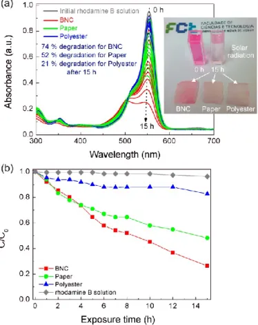
In the present study, the photocatalytic activity of all TiO2 nanostructured films
were evaluated through the rhodamine B degradation efficiency under solar radiation to mimic ambient conditions. The degradation ratio (C/C0) vs. exposure time is presented in
Figure 8, where C is the absorbance of the rhodamine B solution at each exposure time and C0 is the initial solution absorbance. The gradual rhodamine B degradation under
solar radiation could be observed, however the TiO2 film grown on BNC substrate
showed the highest photocatalytic activity. This material reached values of 74 % after 15 h, while the other TiO2 films achieved 52 % and 21 % for the tracing paper and polyester,
respectively. A blank rhodamine B solution was also measured, where it has been observed that the blank solution was not influenced under the solar simulating light source, so all the photocatalytic effect is due to the presence of the catalyst. The photodegradation of rhodamine B has been attributed to the oxidation by different reactive oxygen species [95,96], and its degradation mechanism has been reported in several studies [95-99], including for TiO2 photocatalysts. The degradation under
visible/solar light radiation is the result of the chromophore structure destruction or N-deethylation [99], passing through the formation of intermediate species, that despite being controversial in literature, have in phthalic acid and benzoic acid well accepted
20
intermediates [96,98]. UV/VIS/NIR spectroscopy measurements can be used to infer the mechanisms occurring during rhodamine B photodegradation [99,100].
The photocatalytic activity depends on several properties like band gap, crystallite size, crystalline phase, specific surface area, defects and active facets [5,6,101]. A clear relation between the band gaps of all the materials and their photocatalytic behavior cannot be stated as no significant band gap differences were observed between the cellulose-based materials, and the TiO2 film grown on polyester substrate revealed a
slightly lower value which can be justified by the structural properties of this material. The TiO2 active facets are {110} > {001} > {100} for rutile, and{210} for brookite [13].
In this study, contributions can be expected from active facets in all materials. The mixture of TiO2 phases also can contribute to the increase of photocatalytic performance
[6,102]. In this study, Raman measurements (Figure 4) revealed a mixture of TiO2 phases
(brookite and rutile) for all the materials produced, which can have an expressive contribution to the photocatalytic activity of all materials under solar light simulating source. An analogous study also revealed that the mixture of TiO2 phases (brookite and
rutile) largely increased the photocatalytic performance under UV and solar radiation [6]. In fact, it has been previously described that brookite has higher photocatalytic activity than anatase or rutile [49]. Another study reported a mixture of TiO2 phases, i.e.
anatase-rutile system, which exhibited enhanced visible light activity, promoting the effective transfer of photoexcited electrons and favoring electron–hole separation [90].
The nanocellulose based material demonstrated higher photocatalytic activity than the other materials, thus the structural differences of the TiO2 nanostructured films and
substrates play a key role on the behavior observed. The cellulose-based materials are expected to have higher specific surface area than the ones of the polyester material, in which the latter presented a closed structure with closely packed nanorods [6]. In fact, the cellulose based materials formed a continuous film and presented individual nanostructured particles having nanorod flower-like structures with a more open structure (Figure 2), which can lead to the higher surface area [103]. Regarding the substrates, the nanocellulose substrate has a 3D structure which can effectively enhance the photocatalytic activity. The 3D closed packed cellulose nanofiber network of nanocellulose fully covered by TiO2, not only can provide more active sites for the photoreaction, but also facilitate the
species transport and electrons collection [104].
These materials exhibited resistance to water immersion, and after the photocatalytic experiments even the cellulose-based materials could be recovered and
21
dried as shown on Figure 8 (a). Reusability experiments were carried out for the best photocatalyst, see Figure S5, and it can be observed that the BNC-based material can be reutilized despite the activity deterioration observed over the exposures [105,106]. Thus, these experiments demonstrated that the materials produced, which have been thought to be fully disposable but showing now that they can be reused, are able to effectively degrade pollutant model dyes, and at some point, contribute to the environmental protection, while reducing production costs.
Figure 8. (a) Rhodamine B absorbance spectra at different solar light exposure times up to 15 h. The images
of Rhodamine B solutions at 0 h and after 15 h are presented together with the materials after the photocatalytic experiments. (b) Rhodamine B degradation ratio (C/C0) vs. solar simulating light exposure
time.
Conclusions
TiO2 nanostructured films were successfully grown on low-priced substrates using
microwave synthesis at low temperature, producing flexible and disposable UV photodetectors and photocatalysts with minimal production stages, as it does not require the use of seed layers for the photoactive layer growth, thus reducing the total cost of the device. A mixture of rutile and brookite was identified in all materials, forming
22
continuous films with nanostructures that were arranged distinctively regarding the substrate used. The devices composed by the TiO2 film grown on BNC tended to display
enhanced photosensitivity when compared to the other substrates, nevertheless all devices studied revealed remarkable stability after switching from on to off states several times. The photodetection behaviour and photocatalytic activity were shown to depend on the structural characteristics of the TiO2 nanostructured films and substrates. KPFM data also
demonstrated the enhanced BNC-based material behaviour with the highest contact potential difference shift among the materials investigated. The present work demonstrated that the simple approach developed is an effective and attractive alternative for producing flexible, low-cost, and disposable devices that can be employed in multifunctional applications as photodetectors and photocatalysts.
References
1. Yaghoubi H, Taghavinia N, Alamdari EK (2010) Self cleaning TiO2 coating on polycarbonate: Surface treatment, photocatalytic and nanomechanical properties. Surface and Coatings Technology 204 (9–10):1562-1568. doi:http://dx.doi.org/10.1016/j.surfcoat.2009.09.085 2. Lin J, Heo Y-U, Nattestad A, Sun Z, Wang L, Kim JH, Dou SX (2014) 3D hierarchical rutile TiO 2 and metal-free organic sensitizer producing dye-sensitized solar cells 8.6% conversion
efficiency. Scientific reports 4:5769
3. Dadkhah M, Salavati-Niasari M, Mir N (2014) Synthesis and characterization of TiO2 nanoparticles by using new shape controllers and its application in dye sensitized solar cells. Journal of Industrial and Engineering Chemistry 20 (6):4039-4044.
doi:https://doi.org/10.1016/j.jiec.2014.01.003
4. Sabet M, Salavati-Niasari M (2014) Deposition of cadmium selenide semiconductor nanostructures on TiO2 surface via different chemical methods and investigation of their effects on dye sensitized solar cell efficiency. Materials Science in Semiconductor Processing 27:619-633. doi:https://doi.org/10.1016/j.mssp.2014.07.031
5. Nunes D, Pimentel A, Pinto J, Calmeiro T, Nandy S, Barquinha P, Pereira L, Carvalho P, Fortunato E, Martins R (2016) Photocatalytic behavior of TiO 2 films synthesized by microwave irradiation. Catalysis Today 278:262-270
6. Nunes D, Pimentel A, Santos L, Barquinha P, Fortunato E, Martins R (2017) Photocatalytic TiO2 Nanorod Spheres and Arrays Compatible with Flexible Applications. Catalysts 7 (2):60 7. Bernacka-Wojcik I, Senadeera R, Wojcik PJ, Silva LB, Doria G, Baptista P, Aguas H, Fortunato E, Martins R (2010) Inkjet printed and “doctor blade” TiO2 photodetectors for DNA biosensors. Biosensors and Bioelectronics 25 (5):1229-1234.
doi:http://dx.doi.org/10.1016/j.bios.2009.09.027
8. Bai J, Zhou B (2014) Titanium Dioxide Nanomaterials for Sensor Applications. Chemical Reviews 114 (19):10131-10176. doi:10.1021/cr400625j
9. Liu Z, Li F, Li S, Hu C, Wang W, Wang F, Lin F, Wang H (2015) Fabrication of UV photodetector on TiO2/diamond film. Scientific reports 5
10. Yu X, Zhao Z, Zhang J, Guo W, Qiu J, Li D, Li Z, Mou X, Li L, Li A (2016) Rutile
Nanorod/Anatase Nanowire Junction Array as Both Sensor and Power Supplier for High‐ Performance, Self‐Powered, Wireless UV Photodetector. Small 12 (20):2759-2767
23 11. Chen Z, Xiaohong W, Xuanlin K, Sixing X (2016) High performance flexible ultraviolet
photodetectors based on TiO 2 /graphene hybrid for irradiation monitoring applications. Journal of Micromechanics and Microengineering 26 (7):075003
12. Reyes-Coronado D, Rodríguez-Gattorno G, Espinosa-Pesqueira M, Cab C, De Coss R, Oskam G (2008) Phase-pure TiO2 nanoparticles: anatase, brookite and rutile. Nanotechnology 19 (14):145605
13. Di Paola A, Bellardita M, Palmisano L (2013) Brookite, the least known TiO2 photocatalyst. Catalysts 3 (1):36-73
14. Cao Y, Li X, Bian Z, Fuhr A, Zhang D, Zhu J (2016) Highly photocatalytic activity of brookite/rutile TiO2 nanocrystals with semi-embedded structure. Applied Catalysis B: Environmental 180:551-558. doi:https://doi.org/10.1016/j.apcatb.2015.07.003
15. Liu B, Wang Z, Dong Y, Zhu Y, Gong Y, Ran S, Liu Z, Xu J, Xie Z, Chen D, Shen G (2012) ZnO-nanoparticle-assembled cloth for flexible photodetectors and recyclable photocatalysts. Journal of Materials Chemistry 22 (18):9379-9384. doi:10.1039/C2JM16781F
16. Torras-Rosell A, Johannsen SR, Dirscherl K, Daviðsdóttir S, Jeppesen CS, Louring S, Andersen IH (2017) Comparing the photocatalytic activity of TiO(2) at macro- and microscopic scales. Environmental Science and Pollution Research International 24 (14):12683-12690.
doi:10.1007/s11356-016-7887-3
17. Wu M-C, Liao H-C, Cho Y-C, Tóth G, Chen Y-F, Su W-F, Kordás K (2013) Photo-Kelvin probe force microscopy for photocatalytic performance characterization of single filament of TiO 2 nanofiber photocatalysts. Journal of Materials Chemistry A 1 (18):5715-5720
18. Wu M-C, Liao H-C, Cho Y-C, Hsu C-P, Lin T-H, Su W-F, Sápi A, Kukovecz Á, Kónya Z, Shchukarev A, Sarkar A, Larsson W, Mikkola J-P, Mohl M, Tóth G, Jantunen H, Valtanen A, Huuhtanen M, Keiski RL, Kordás K (2013) Photocatalytic activity of nitrogen-doped TiO2-based nanowires: a photo-assisted Kelvin probe force microscopy study. Journal of Nanoparticle Research 16 (1):1-11. doi:10.1007/s11051-013-2143-y
19. Vicente AT, Araújo A, Gaspar D, Santos L, Marques AC, Mendes MJ, Pereira L, Fortunato E, Martins R (2017) Optoelectronics and Bio Devices on Paper Powered by Solar Cells. In: Nanostructured Solar Cells. InTech,
20. T. Vicente A, Araujo A, Mendes MJ, Nunes D, Oliveira MJ, Sanchez-Sobrado O, Ferreira MP, Aguas H, Fortunato E, Martins R (2018) Multifunctional cellulose-paper for light harvesting and smart sensing applications. Journal of Materials Chemistry C. doi:10.1039/C7TC05271E
21. Gama M, Dourado F, Bielecki S (2016) Bacterial Nanocellulose: From Biotechnology to Bio-Economy. Elsevier Science,
22. Barros AD, Albertin KF, Miyoshi J, Doi I, Diniz JA (2010) Thin titanium oxide films deposited by e-beam evaporation with additional rapid thermal oxidation and annealing for ISFET applications. Microelectronic Engineering 87 (3):443-446.
doi:http://dx.doi.org/10.1016/j.mee.2009.06.020
23. Zheng J, Bao S, Guo Y, Jin P (2014) TiO2 films prepared by DC reactive magnetron sputtering at room temperature: Phase control and photocatalytic properties. Surface and Coatings Technology 240:293-300. doi:http://dx.doi.org/10.1016/j.surfcoat.2013.12.044 24. Dongale TD, Shinde SS, Kamat RK, Rajpure KY (2014) Nanostructured TiO2 thin film memristor using hydrothermal process. Journal of Alloys and Compounds 593:267-270. doi:http://dx.doi.org/10.1016/j.jallcom.2014.01.093
25. Lee S-H, Kang M, Cho SM, Han GY, Kim B-W, Yoon KJ, Chung C-H (2001) Synthesis of TiO2 photocatalyst thin film by solvothermal method with a small amount of water and its
photocatalytic performance. Journal of Photochemistry and Photobiology A: Chemistry 146 (1– 2):121-128. doi:http://dx.doi.org/10.1016/S1010-6030(01)00553-6
26. Salavati-Niasari M, Javidi J, Dadkhah M (2013) Ball milling synthesis of silica nanoparticle from rice husk ash for drug delivery application. Combinatorial chemistry & high throughput screening 16 (6):458-462
24 27. Pimentel A, Rodrigues J, Duarte P, Nunes D, Costa F, Monteiro T, Martins R, Fortunato E (2015) Effect of solvents on ZnO nanostructures synthesized by solvothermal method assisted by microwave radiation: a photocatalytic study. Journal of Materials Science 50 (17):5777-5787 28. Nunes D, Pimentel A, Barquinha P, Carvalho PA, Fortunato E, Martins R (2014) Cu2O polyhedral nanowires produced by microwave irradiation. Journal of Materials Chemistry C 2 (30):6097-6103. doi:10.1039/C4TC00747F
29. Bose A, Sreemany M, Bysakh S (2011) Role of TiO2 Seed Layer Thickness on the Nanostructure Evolution and Phase Transformation Behavior of Sputtered PZT Thin Films During Post‐Deposition Air‐Annealing. Journal of the American Ceramic Society 94 (11):4066-4077
30. Bielecki S, Krystynowicz A, Turkiewicz M, Kalinowska H (2005) Bacterial Cellulose. In: Biopolymers Online. Wiley-VCH Verlag GmbH & Co. KGaA. doi:10.1002/3527600035.bpol5003 31. Brown JRM (1989) Bacterial cellulose. Cellulose: Structural and Functional Aspects. Ellis Horwood Ltd, Chichestr, UK
32. Costa V, Costa A, Amaral M, Oliveira C, Gama M, Dourado F, Simões R (2016) Effect of hot calendering on physical properties and water vapor transfer resistance of bacterial cellulose films. Journal of Materials Science 51 (21):9562-9572
33. Pimentel A, Samouco A, Nunes D, Araújo A, Martins R, Fortunato E (2017) Ultra-Fast Microwave Synthesis of ZnO Nanorods on Cellulose Substrates for UV Sensor Applications. Materials 10 (11):1308
34. Kraus W, Nolze G (1996) POWDER CELL - a program for the representation and manipulation of crystal structures and calculation of the resulting X-ray powder patterns. Journal of Applied Crystallography 29 (3):301-303. doi:doi:10.1107/S0021889895014920 35. Pearson WB, Villars P, Calvert LD (1985) Pearson's handbook of crystallographic data for intermetallic phases. vol vol. 2. American Society for Metals,
36. Schneider CA, Rasband WS, Eliceiri KW (2012) NIH Image to ImageJ: 25 years of image analysis. Nature Methods 9:671-675
37. Nunes D, Calmeiro TR, Nandy S, Pinto JV, Pimentel A, Barquinha P, Carvalho PA, Walmsley JC, Fortunato E, Martins R (2016) Charging effects and surface potential variations of Cu-based nanowires. Thin Solid Films 601:45-53. doi:https://doi.org/10.1016/j.tsf.2015.11.077
38. Panigrahi S, Calmeiro T, Martins R, Nunes D, Fortunato E (2016) Observation of Space Charge Dynamics Inside an All Oxide Based Solar Cell. ACS Nano 10 (6):6139-6146. doi:10.1021/acsnano.6b02090
39. Santos L, Nunes D, Calmeiro T, Branquinho R, Salgueiro D, Barquinha P, Pereira L, Martins R, Fortunato E (2015) Solvothermal Synthesis of Gallium–Indium-Zinc-Oxide Nanoparticles for Electrolyte-Gated Transistors. ACS Applied Materials & Interfaces 7 (1):638-646.
doi:10.1021/am506814t
40. Du Y, Zhang MS, Wu J, Kang L, Yang S, Wu P, Yin Z (2003) Optical properties of SrTiO3 thin films by pulsed laser deposition. Applied Physics A 76 (7):1105-1108. doi:10.1007/s00339-002-1998-z
41. Tauc J (1968) Optical properties and electronic structure of amorphous Ge and Si. Materials Research Bulletin 3 (1):37-46. doi:http://dx.doi.org/10.1016/0025-5408(68)90023-8
42. Pimentel A, Ferreira SH, Nunes D, Calmeiro T, Martins R, Fortunato E (2016) Microwave Synthesized ZnO Nanorod Arrays for UV Sensors: A Seed Layer Annealing Temperature Study. Materials 9 (4):299
43. Wu M-C, Liao H-C, Cho Y-C, Hsu C-P, Lin T-H, Su W-F, Sápi A, Kukovecz Á, Kónya Z,
Shchukarev A (2014) Photocatalytic activity of nitrogen-doped TiO2-based nanowires: a photo-assisted Kelvin probe force microscopy study. Journal of nanoparticle research 16 (1):1-11 44. Zhou W, Liu X, Cui J, Liu D, Li J, Jiang H, Wang J, Liu H (2011) Control synthesis of rutile TiO2 microspheres, nanoflowers, nanotrees and nanobelts via acid-hydrothermal method and their optical properties. CrystEngComm 13 (14):4557-4563. doi:10.1039/C1CE05186E
25 45. Wang M, Li Q, Yu H, Hur SH, Kim EJ (2013) Phase-controlled preparation of TiO2 films and micro(nano)spheres by low-temperature chemical bath deposition. Journal of Alloys and Compounds 578:419-424. doi:http://dx.doi.org/10.1016/j.jallcom.2013.06.065
46. Andreia A, Ana P, Maria João O, Manuel JM, Ricardo F, Elvira F, Hugo Á, Rodrigo M (2017) Direct growth of plasmonic nanorod forests on paper substrates for low-cost flexible 3D SERS platforms. Flexible and Printed Electronics 2 (1):014001
47. Manekkathodi A, Lu M-Y, Wang CW, Chen L-J (2010) Direct Growth of Aligned Zinc Oxide Nanorods on Paper Substrates for Low-Cost Flexible Electronics. Advanced Materials 22 (36):4059-4063. doi:10.1002/adma.201001289
48. Pimentel A, Araújo A, Coelho B, Nunes D, Oliveira M, Mendes M, Águas H, Martins R, Fortunato E (2017) 3D ZnO/Ag Surface-Enhanced Raman Scattering on Disposable and Flexible Cardboard Platforms. Materials 10 (12):1351
49. Wang Y, Li L, Huang X, Li Q, Li G (2015) New insights into fluorinated TiO2 (brookite, anatase and rutile) nanoparticles as efficient photocatalytic redox catalysts. RSC Advances 5 (43):34302-34313. doi:10.1039/C4RA17076H
50. Aydın C, Benhaliliba M, Al-Ghamdi A, Gafer Z, El-Tantawy F, Yakuphanoglu F (2013) Determination of optical band gap of ZnO:ZnAl2O4 composite semiconductor nanopowder materials by optical reflectance method. J Electroceram 31 (1-2):265-270. doi:10.1007/s10832-013-9829-5
51. Yu J-G, Yu H-G, Cheng B, Zhao X-J, Yu JC, Ho W-K (2003) The Effect of Calcination Temperature on the Surface Microstructure and Photocatalytic Activity of TiO2 Thin Films Prepared by Liquid Phase Deposition. The Journal of Physical Chemistry B 107 (50):13871-13879. doi:10.1021/jp036158y
52. Wu J-M, Shih HC, Wu W-T (2006) Formation and photoluminescence of single-crystalline rutile TiO2 nanowires synthesized by thermal evaporation. Nanotechnology 17 (1):105 53. Ramana C, Smith R, Hussain O (2003) Grain size effects on the optical characteristics of pulsed‐laser deposited vanadium oxide thin films. physica status solidi (a) 199 (1):R4-R6 54. Migas DB, Filonov AB, Borisenko VE, Skorodumova NV (2014) Orientation effects in morphology and electronic properties of anatase TiO2 one-dimensional nanostructures. I. Nanowires. Physical Chemistry Chemical Physics 16 (20):9479-9489. doi:10.1039/C3CP54988G 55. Enrı ́quez JP, Mathew X (2003) Influence of the thickness on structural, optical and electrical properties of chemical bath deposited CdS thin films. Solar Energy Materials and Solar Cells 76 (3):313-322. doi:http://dx.doi.org/10.1016/S0927-0248(02)00283-0
56. Pereira L, Barquinha P, Fortunato E, Martins R, Kang D, Kim CJ, Lim H, Song I, Park Y (2008) High k dielectrics for low temperature electronics. Thin Solid Films 516 (7):1544-1548.
doi:http://dx.doi.org/10.1016/j.tsf.2007.03.088
57. Chen H, Liu K, Hu L, Al-Ghamdi AA, Fang X (2015) New concept ultraviolet photodetectors. Materials Today 18 (9):493-502. doi:http://dx.doi.org/10.1016/j.mattod.2015.06.001
58. Mor GK, Carvalho MA, Varghese OK, Pishko MV, Grimes CA (2004) A room-temperature TiO2-nanotube hydrogen sensor able to self-clean photoactively from environmental contamination. Journal of Materials Research 19 (02):628-634
59. Fryxell GE, Cao G (2012) Environmental Applications of Nanomaterials: Synthesis, Sorbents and Sensors. Imperial College Press,
60. Wang Z, Gu Y, Qi J, Lu S, Li P, Lin P, Zhang Y (2015) Size dependence and UV irradiation tuning of the surface potential in single conical ZnO nanowires. RSC Advances 5 (52):42075-42080. doi:10.1039/C5RA04467G
61. Soci C, Zhang A, Xiang B, Dayeh SA, Aplin D, Park J, Bao X, Lo Y-H, Wang D (2007) ZnO nanowire UV photodetectors with high internal gain. Nano letters 7 (4):1003-1009 62. Sensor Characteristics and Physical Effects (2008). In: Kalantar-zadeh K, Fry B (eds)
Nanotechnology-Enabled Sensors. Springer US, Boston, MA, pp 13-62. doi:10.1007/978-0-387-68023-1_2
26 63. Fu Y, Cao W (2006) Preparation of transparent TiO2 nanocrystalline film for UV sensor. Chinese Science Bulletin 51 (14):1657-1661. doi:10.1007/s11434-006-2022-3
64. Li Y-R, Wan C-Y, Chang C-T, Tsai W-L, Huang Y-C, Wang K-Y, Yang P-Y, Cheng H-C (2015) Thickness effect of NiO on the performance of ultraviolet sensors with p-NiO/n-ZnO nanowire heterojunction structure. Vacuum 118:48-54.
doi:http://dx.doi.org/10.1016/j.vacuum.2015.01.018
65. Dufresne A (2013) Nanocellulose: a new ageless bionanomaterial. Materials Today 16 (6):220-227. doi:http://dx.doi.org/10.1016/j.mattod.2013.06.004
66. Melitz W, Shen J, Kummel AC, Lee S (2011) Kelvin probe force microscopy and its application. Surface Science Reports 66 (1):1-27.
doi:http://dx.doi.org/10.1016/j.surfrep.2010.10.001
67. Liscio A, Palermo V, Samorì P (2010) Nanoscale quantitative measurement of the potential of charged nanostructures by electrostatic and Kelvin probe force microscopy: unraveling electronic processes in complex materials. Accounts of chemical research 43 (4):541-550 68. Wu Z, Qi J, Li F, Zhu X, Wang Z, Zhang G, Zhang Y (2016) The coupling influence of UV illumination and strain on the surface potential distribution of a single ZnO micro/nano wire. Nano Research:1-9. doi:10.1007/s12274-016-1143-5
69. Li Y, Liu Y, Wang J, Uchaker E, Zhang Q, Sun S, Huang Y, Li J, Cao G (2013) Titanium alkoxide induced BiOBr-Bi2WO6 mesoporous nanosheet composites with much enhanced
photocatalytic activity. Journal of Materials Chemistry A 1 (27):7949-7956. doi:10.1039/C3TA10940B
70. Ghiyasiyan-Arani M, Salavati-Niasari M, Naseh S (2017) Enhanced photodegradation of dye in waste water using iron vanadate nanocomposite; ultrasound-assisted preparation and characterization. Ultrasonics Sonochemistry 39:494-503.
doi:https://doi.org/10.1016/j.ultsonch.2017.05.025
71. Monsef R, Ghiyasiyan-Arani M, Salavati-Niasari M (2018) Application of ultrasound-aided method for the synthesis of NdVO4 nano-photocatalyst and investigation of eliminate dye in contaminant water. Ultrasonics Sonochemistry 42:201-211.
doi:https://doi.org/10.1016/j.ultsonch.2017.11.025
72. Ghiyasiyan-Arani M, Salavati-Niasari M, Masjedi-Arani M, Mazloom F (2018) An easy sonochemical route for synthesis, characterization and photocatalytic performance of
nanosized FeVO4 in the presence of aminoacids as green capping agents. Journal of Materials Science: Materials in Electronics 29 (1):474-485. doi:10.1007/s10854-017-7936-9
73. Mazloom F, Masjedi-Arani M, Ghiyasiyan-Arani M, Salavati-Niasari M (2016) Novel sodium dodecyl sulfate-assisted synthesis of Zn3V2O8 nanostructures via a simple route. Journal of Molecular Liquids 214:46-53. doi:https://doi.org/10.1016/j.molliq.2015.11.033
74. Ghiyasiyan-Arani M, Masjedi-Arani M, Ghanbari D, Bagheri S, Salavati-Niasari M (2016) Novel chemical synthesis and characterization of copper pyrovanadate nanoparticles and its influence on the flame retardancy of polymeric nanocomposites. Scientific Reports 6:25231. doi:10.1038/srep25231
75. Ghiyasiyan-Arani M, Masjedi-Arani M, salavati-Niasari M (2016) Size controllable synthesis of cobalt vanadate nanostructures with enhanced photocatalytic activity for the degradation of organic dyes. Journal of Molecular Catalysis A: Chemical 425:31-42.
doi:https://doi.org/10.1016/j.molcata.2016.09.023
76. Ghiyasiyan-Arani M, Masjedi-Arani M, Salavati-Niasari M (2016) Novel Schiff base ligand-assisted in-situ synthesis of Cu3V2O8 nanoparticles via a simple precipitation approach. Journal of Molecular Liquids 216:59-66. doi:https://doi.org/10.1016/j.molliq.2015.12.100 77. Ghiyasiyan-Arani M, Masjedi-Arani M, Salavati-Niasari M (2015) Simple Precipitation Synthesis of Pure Cu3V2O8 Nanoparticles and Investigation of their Optical Properties. Journal of Nanostructures 5 (4):437-441. doi:10.7508/jns.2015.04.015
78. Ghiyasiyan-Arani M, Masjedi-Arani M, Salavati-Niasari M (2016) Facile synthesis, characterization and optical properties of copper vanadate nanostructures for enhanced
27 photocatalytic activity. Journal of Materials Science: Materials in Electronics 27 (5):4871-4878. doi:10.1007/s10854-016-4370-3
79. Szilágyi IM, Fórizs B, Rosseler O, Szegedi Á, Németh P, Király P, Tárkányi G, Vajna B, Varga-Josepovits K, László K, Tóth AL, Baranyai P, Leskelä M (2012) WO3 photocatalysts: Influence of structure and composition. Journal of Catalysis 294:119-127.
doi:https://doi.org/10.1016/j.jcat.2012.07.013
80. Elango G, Roopan SM (2016) Efficacy of SnO2 nanoparticles toward photocatalytic degradation of methylene blue dye. Journal of Photochemistry and Photobiology B: Biology 155:34-38. doi:https://doi.org/10.1016/j.jphotobiol.2015.12.010
81. Pimentel A, Rodrigues J, Duarte P, Nunes D, Costa FM, Monteiro T, Martins R, Fortunato E (2015) Effect of solvents on ZnO nanostructures synthesized by solvothermal method assisted by microwave radiation: a photocatalytic study. Journal of Materials Science 50 (17):5777-5787. doi:10.1007/s10853-015-9125-7
82. Liu P, Zhang J, Gao D, Ye W (2017) Efficient visible light-induced degradation of rhodamine B by W(NxS1−x)2 nanoflowers. Scientific Reports 7:40784. doi:10.1038/srep40784
https://www.nature.com/articles/srep40784#supplementary-information
83. Reyes-Coronado D, Rodríguez-Gattorno G, Espinosa-Pesqueira M, Cab C, de Coss Rd, Oskam G (2008) Phase-pure TiO2 nanoparticles: anatase, brookite and rutile. Nanotechnology 19 (14):145605
84. Karunakaran C, Senthilvelan S (2006) Fe2O3-photocatalysis with sunlight and UV light: Oxidation of aniline. Electrochemistry Communications 8 (1):95-101.
doi:https://doi.org/10.1016/j.elecom.2005.10.034
85. Kazuhito H, Hiroshi I, Akira F (2005) TiO 2 Photocatalysis: A Historical Overview and Future Prospects. Japanese Journal of Applied Physics 44 (12R):8269
86. Mecha AC, Onyango MS, Ochieng A, Jamil TS, Fourie CJS, Momba MNB (2016) UV and solar light photocatalytic removal of organic contaminants in municipal wastewater. Separation Science and Technology 51 (10):1765-1778. doi:10.1080/01496395.2016.1178290
87. Leong KH, Monash P, Ibrahim S, Saravanan P (2014) Solar photocatalytic activity of anatase TiO2 nanocrystals synthesized by non-hydrolitic sol–gel method. Solar Energy 101 (Supplement C):321-332. doi:https://doi.org/10.1016/j.solener.2014.01.006
88. Justicia I, Ordejón P, Canto G, Mozos JL, Fraxedas J, Battiston GA, Gerbasi R, Figueras A (2002) Designed Self‐Doped Titanium Oxide Thin Films for Efficient Visible‐Light Photocatalysis. Advanced Materials 14 (19):1399-1402
89. Borges ME, Sierra M, Cuevas E, García RD, Esparza P (2016) Photocatalysis with solar energy: Sunlight-responsive photocatalyst based on TiO2 loaded on a natural material for wastewater treatment. Solar Energy 135 (Supplement C):527-535.
doi:https://doi.org/10.1016/j.solener.2016.06.022
90. Fagan R, McCormack DE, Dionysiou DD, Pillai SC (2016) A review of solar and visible light active TiO2 photocatalysis for treating bacteria, cyanotoxins and contaminants of emerging concern. Materials Science in Semiconductor Processing 42 (Part 1):2-14.
doi:https://doi.org/10.1016/j.mssp.2015.07.052
91. Miranda-García N, Suárez S, Sánchez B, Coronado J, Malato S, Maldonado MI (2011) Photocatalytic degradation of emerging contaminants in municipal wastewater treatment plant effluents using immobilized TiO 2 in a solar pilot plant. Applied Catalysis B:
Environmental 103 (3):294-301
92. Etacheri V, Di Valentin C, Schneider J, Bahnemann D, Pillai SC (2015) Visible-light activation of TiO2 photocatalysts: Advances in theory and experiments. Journal of Photochemistry and Photobiology C: Photochemistry Reviews 25 (Supplement C):1-29.