Physical Properties of Sputtered Indium-doped ZnO Films Deposited on Flexible
Transparent Substrates
Hector Eduardo Silva-Lopeza* , Becerril Silva Marcelinoa, Angel Guillen-Cervantesa, Orlando Zelaya-Angela, Rafael Ramirez-Bonb
Received: March 24, 2018; Revised: July 07, 2018; Accepted: August 16, 2018
Indium-doped zinc oxide (IZO) polycrystalline thin films were grown on polyethylene terephthalate
(PET), polyethylene naphthalate (PEN), and as reference on 7059 Corning glass substrates at room
temperature by radio frequency magnetron sputtering from a target prepared with a mixture of ZnO
and In2O3 powders. The structural, optical, and electrical properties of the films were analyzed and
compared. The IZO polycrystalline films showed n-type conductivity. The electrical resistivity drops significantly, and the carrier concentration increases as a consequence of In incorporation within the ZnO crystalline lattice. In both cases the changes are of several orders of magnitude. The resistivity obtained was 3.1 ± 0.5 x 10⁻³ Ω-cm for an IZO sample grown on PET with a carrier concentration of
3.1 ± 0.7 x 1020 cm-3, the best mobility obtained was 27.7 ± 0.8 cm2V-1s-1 for an IZO sample grown
on PEN. From the results, we conclude that n-type IZO polycrystalline films with high transmittance, high mobility and low resistivity were obtained on flexible transparent substrates.
Keywords: Flexible transparent substrates, PET, PEN, Indium-doped zinc oxide, polycrystalline thin films.
*e-mail: hsl@fis.cinvestav.mx
1. Introduction
Transparent conducting oxide (TCO) materials such as indium tin oxide (ITO) have been of interest due to their high
electrical conductivity and optical transparency. However,
due to the scarcity of In reserves1, candidates for ITO
replacements are necessary especially when In concentration is as high as 90% in commercial ITO glasses. ZnO-based
transparent electrodes have been extensively investigated as potential substitutes2,3. Conductive ZnO films have aroused
increasing interest due to their applications in solar cells, gas sensors, varistors and light emitting diodes4-6. However,
the electrical conductivity of ZnO is low compared to most TCO electrodes. To increase ZnO conductivity, group III
elements (Al, Ga, and In) have been used as substitutional
dopants for Zn, with Al-doped ZnO (AZO) as one of the
most extensively TCO studied materials7,8. In this regard,
Indium is an attractive dopant for n-type ZnO because has less reactivity and greater oxidation-resistance relative to
Al. Therefore, Indium-doped zinc oxide (IZO) films are a promising alternative for ITO films. Nevertheless, the literature about IZO films9-11 is not as abundant as in the case
of AZO films.2-4. On the other hand, in energy conversion
technology the deposition on flexible substrates will be a
reliable solution12. Some advantages of these substrates
are: cost, they are cheaper than glass, flexibility and lighter
weight13,14, besides plastic substrates are compatible with
low temperature manufacturing processes; for instance, the thin film transistor manufacture, for the development of flexible large-area electronics15,16, where TCOs deposited
at low temperature and with high mobility are required17.
Plastic materials which have been used for substrate purposes
are: acrylic, polyethylene terephthalate (PET), polyethylene
naphthalate (PEN), polycarbonate, etc.,12-15,17-19. Due to
their good optical and mechanical properties and easy processability, PEN and PET materials stand out as substrates
for applications in flexible electronics. For this work, we deposited IZO thin films on PEN, PET, and as reference on alkali-free borosilicate glass substrates by radio frequency (rf) magnetron sputtering. We investigated the structural, optical, and electrical properties of the sputtered thin films grown at room temperature (RT). The electrical resistivity of IZO thin films decreases by four orders of magnitude; meanwhile its carrier concentration increases three to four orders of magnitude as compared with an undoped ZnO reference film. Furthermore, the IZO film deposited on a
PEN substrate has excellent transmittance in the visible
range and very high mobility figures.
2. Experimental Details
Indium-doped zinc oxide (IZO) films were deposited onto, PET, PEN, and as reference a ZnO film and an IZO aDepartamento de Física, Centro de Investigación y de Estudios Avanzados, Instituto Politecnico
Nacional (IPN), Apartado Postal 14-740, D.F. 07300, México
film were grown on 7059 alkali-free borosilicate (Corning
Glass) substrates at RT in a rf magnetron sputtering system
equipped with a water-cooled cathode. The experimental conditions for the growth provide ZnO samples with high
structural and electrical properties as reported previously8.
The rf power employed was 20 W and the distance between the target and substrate 3.5 cm. The chamber was evacuated to a pressure of 1.33 mPa before the addition of pure Ar gas. The total Ar pressure was kept at 1.33x10⁻¹ Pa during the
deposition process. The films were deposited for 45 min. The IZO target, which has an area of 4.92 cm2 and a weight of 5.2
grams was prepared from 4 grams of ZnO (purity, 99.99% from Sigma-Aldrich) and 1.2 grams of In2O3 (Sigma-Aldrich,
purity 99.99%) powders. Oxide powders were mixed and compressed with 15 Tons for 8 hours to form a 2 inches diameter target. The ZnO target used for the growth of the ZnO reference film, was composed only with 5.2 grams of zinc oxide powder, target was compressed at 15 Tons for 8 hours. The ZnO and IZO reference films deposited on glass were labeled as ZnO and IZO1 respectively. IZO
films grown on PET and PEN were labeled IZO2 and IZO3
respectively (see Table 1). The growths were performed
under identical experimental conditions to evaluate the
structural, optical, and electrical properties of IZO films deposited on plastic substrates. The crystalline structure of the films was determined by X-ray diffraction (XRD) using a SIEMENS D-5000 equipment, with the Cu-Kα line (1.5406 Å). The film thicknesses were estimated by a KLA Tencor P15 profiler. The optical transmittance spectra of the films were measured in an UNICAM 8700 spectrophotometer in the 200-1000 nm range. IZO thin films and plastic substrates roughness measurements were obtained with an Atomic Force Microscopy (AFM) equipment model Autoprobe CP from Veeco Metrology Group. Atomic concentration measurements of the samples were evaluated by Energy Dispersive Spectroscopy (EDS) with an X-Flash 5010 detector from Bruker installed in a Jeol Scanning Electron Microscope model JSM-3600. To determine the elemental atomic concentration of O, Zn, and In in the films, a set of ZnO and IZO samples were deposited on silicon substrates
to avoid oxygen contribution from the PET, PEN, and glass
in the EDS measurements. The silicon substrates were placed aside of the PET, PEN, and glass substrates in each growth.
The resistivity, carrier concentration, mobility and type of
conductivity of the films were measured at RT using the Van der Pauw method in a Hall effect equipment. To perform electrical measurements, high purity Silver Paint (Alfa Aesar ˃99 %) electrodes were deposited on the films.
3. Experimental Results and Discussion
Fig. 1 exhibits a diffractogram of an IZO representative sample. The XRD pattern indicates the films are polycrystalline with hexagonal wurtzite structure20. A preferred orientation
along the (002) direction is observed. The right inset in Fig. 1 shows, both, the (002) interplanar distance (ID) of the samples estimated from the XRD patterns and the Bragg angle as a function of the deposited sample. ZnOb corresponds to the
bulk standard data taken from literature21, and the ZnO sample
is the undoped reference film grown on a glass substrate.
Based on the ZnOb standard position in the graph, note that
the (002) reflection corresponding to the studied samples shifts to lower 2( angles while the ID values increase. Similar tendency is observed for the (102) and (103) XRD reflections showed in the left inset in Fig. 1, the 2θ values of the (102) and the (103) diffraction peaks decrease in the samples. This behavior suggests expansion in the ZnO lattice. In the case of the ZnO reference sample a larger ID value compared
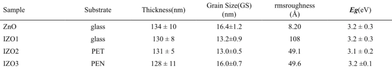
Table 1. Thickness, Grain size, roughness and band gap experimental data of the ZnO and IZO films grown on glass, PET and PEN by
rf magnetron sputtering at RT.
Sample Substrate Thickness(nm) Grain Size(GS)
(nm)
rmsroughness
(Å) Eg(eV)
ZnO glass 134 ± 10 16.4±1.2 8.20 3.2 ± 0.3
IZO1 glass 130 ± 8 13.2±0.9 108 3.2 ± 0.3
IZO2 PET 131 ± 5 13.0±0.5 49.1 3.1 ± 0.2
IZO3 PEN 128 ± 11 16.0±0.7 49.6 3.2 ±0.1
Figure 1. XRD diffractogram of an IZO representative film. The
with the ZnOb standard is related with the difference in the
linear expansion coefficient between the film and substrate (corning glass). The linear expansion coefficient for bulk zinc
oxide 21 is about two orders of magnitude larger than that
corresponding to the glass substrate. In despite the growth is performed at RT, due to plasma and the rf power in the
magnetron sputtering system the temperature increases about
5 °C. Therefore, after growth, when the film and the substrate thermalize the ZnO film lattice remains expanded. For the IZO samples the difference in ID values can be explained in terms of the difference in the atomic radii between Zn and In atoms. The In atomic radii (81 pm) is larger than the Zn one (74 pm). Thus, the substitution of Zn atoms by In atoms in the films increases the lattice parameters.
From the full width at half maximum (FWHM) of the (002) XRD diffraction peak, the grain size (GS) of the films was estimated using the Debye-Scherrer formula: GS=ελ/ βcosθ, where GS refers to grain size, ε is a constant with a
value of 0.94, λ is the Cu-Kα wavelength of the XRD source, β is the FWHM of the diffraction peak measured in radians,
and θ is the Bragg angle8. The films have grain size between
13 and 16.4 nm. It was previously reported that small grain size could be due to the fact that samples were grown at
RT without a post-growth thermal annealing9. GS values
and thickness of the IZO films are displayed in Table 1. A
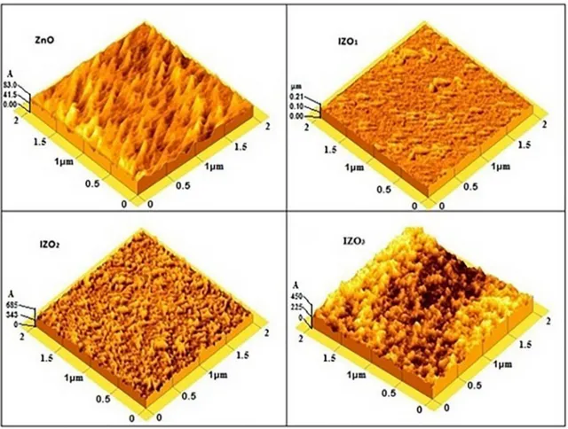
detailed analysis of the surface morphology of the samples
was made by AFM. 2 µm × 2 µm images of ZnO and IZO samples prepared at RT are depicted in Fig. 2. There is an
evident change of roughness in the IZO1, IZO2, and IZO3
samples compared to ZnO. The ZnO sample presents root mean square (rms) roughness of 8.20 Å while the samples
IZO1, IZO2, and IZO3 have rms values of 108, 49.1, and
49.6 Å, respectively (see Table 1). This higher value in
roughness for IZO samples could be probably due to the
incorporation of indium in the films. Figure 3 compares the optical transmittance of the films and the PEN, PET and glass substrates. The average transmittance in the 400-1000 nm wavelength range of the undoped ZnO film was 78% while
for the IZO1, IZO2, and IZO3 films average transmittance
values were 79%, 80%, and 82%, respectively. It is worth to mention that sample with the highest transmittance is the sample with the largest GS. It is well known that samples with
reduced GS have poor transparency due to light scattering from grain frontiers7. The ripples observed in the transmission
signal for the IZO2 sample are effect of the structure of the PET substrate, as corroborated from the PET transmission
spectrum shown in Fig. 3. The direct optical band gap Eg was calculated using Cody´s relationship22: α2 = A(hv - Eg) where α is the optical absorption coefficient, hv is the photon energy, A is a constant, and Eg the band gap energy. Absorption coefficients of the films for different wavelength have been calculated from the transmittance and reflection data. Table 1 summarizes the energy band gap Eg of the
films studied in this work. The data were measured several times at different points on the surface of the samples and the standard deviation values were calculated as reported. Despite the expansion of the lattice, Eg conserves the zinc
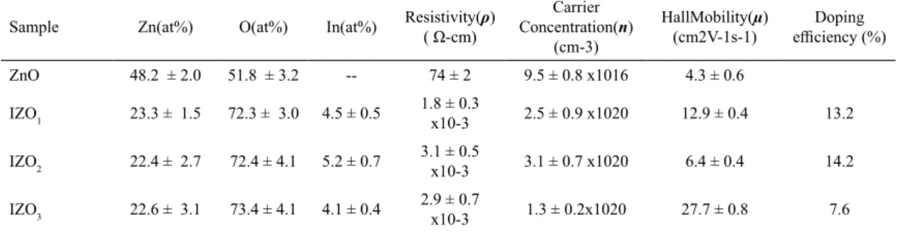
oxide value in bulk. The analysis of the chemical composition measured by EDS (Table 2) indicates that indium atoms were incorporated into the ZnO films at 4.5 at. % for IZO1
sample, 5.2 at. % in IZO2 and 4.1 at. % for IZO3 sample,
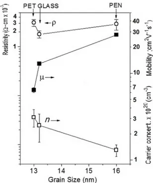
the In incorporation in the ZnO lattice was of the same order in despite of the type of substrate. Fig. 4 and Table 2 show the behavior of the resistivity, carrier concentration, and mobility of the IZO samples studied in this work as a
function of the substrate and GS. Note the incorporation of indium into the IZO films has a strong effect in the electrical measurements. The undoped ZnO film has a resistivity of 74 ± 2 Ω-cm (not shown in the graph but in the Table 2) while
samples IZO1, IZO2, and IZO3 have resistivity of 1.8 x 10⁻³,
3.1 x 10⁻³, and 2.9 x 10⁻³ Ω-cm, respectively. After indium
doping process, every In3+ contributes with an extra electron
to the number of charge carries7 although, resistivity of the
IZO samples decreases compared with the undoped ZnO
film. The resistivity for IZO1, IZO2, and IZO3 films drops
four orders of magnitude, compared with that of the ZnO reference film deposited on glass. On the other hand, the carrier concentration, according to the graph in Fig. 4 and results in Table 2, varies from 9.5 x 1016 cm-3 in ZnO to 3.1
x 1020 cm-3 in IZO
2 film grown on the PET substrate. The
ZnO and IZO films are n-type. The Hall mobility μ increases
after In doping and shows a maximum value of 27.7 cm2 V-1
s-1 in sample IZO
3 which was deposited on PEN. This higher
Hall mobility was measured in the sample with a lower carrier concentration. Mobility trend can be explained as follows: low doping levels decrease the carrier concentration in the IZO films with a consequent reduction in electron scattering effects3, thus the Hall mobility increases. Fig. 4
also indicates that if the GS decreases, ( decreases while n increases, which means that higher doping levels decrease
the grain size in the samples for the experimental conditions
reported in this work. It has been observed that the planarity of surface strongly influences the physical properties of
deposited material23,24. Although, the rms roughness of the
surface of substrates was determined by AFM: glass 0.36 ± 0.04 nm, PET 2.3 ± 0.6 nm, and PEN 2.5 ± 0.4 nm. In our
experiments, the GS of IZO samples decreases when rms roughness of the substrate also decreases affecting μ figures, which, according with the above discussion, corroborates the influence substrate surface has on physical properties
Figure 3. The optical transmittance of the ZnO, IZO films and the
PEN, PET and glass substrates.
Figure 4. Resistivity (ρ), Mobility (() and Carrier concentration (n) behavior as a function of the grain size (GS) for the IZO samples.
of deposited films. Doping efficiency for the IZO samples was calculated considering the inset in Fig. 4, the unit cell parameters were taken from reference21. The ZnO unit cell
volume (V) calculated was V= 4.76 x 10⁻²³ cm3, taking into
consideration 4 atoms per unit cell (2 oxygen atoms and 2 of zinc), the number of Zn atoms per cm3 (#/V) is 4.2 x 10²²
at.cm-3. For n- type doping, indium occupies zinc sites. The
percentage of Indium in the IZO1 sample is 4.5 at.%. By assuming that all the In atoms enter substitutionally in the ZnO lattice, that is, the number of In atoms in interstitials
positions and in antisites is neglected. Then, the number of atoms that the In should occupy for a 100% doping efficiency is, (an electron per each In atom), ~ 0.045 x 4.2 x 1022 cm-3
= 0.189 x 1022 cm-3 = 1.89 x 1021 cm-3. Assuming also that
all the donors are ionized at room temperature, this number
would be the expected majority carrier density. However, only 2.5 x 1020 cm-3 active carriers were measured in the
Hall experiments. Thus, the doping efficiency calculated
for IZO1 is 2.5 x 10²⁰/1.89 x 1021 = 0.132 = 13.2%. For
IZO2 the efficiency results 14.2%, and for IZO3 7.6%. Note
doping efficiency is better for PET substrates an important
factor considering the impact plastic substrates have in the
semiconductor industry, doping efficiency values are listed in Table 2. It is worth to mention that the low resistivity figures reported in this work were measured in samples grown at RT by rf magnetron sputtering on flexible substrates and are comparable to those grown with different conditions
on conducting substrates and/or in post-growth annealed
samples (see Table 3)25-31.
4. Conclusion
In summary, the structural, optical, and electrical properties
of IZO films deposited under identical growth conditions
at RT by rf magnetron sputtering on glass, PET and PEN
substrates were investigated. IZO samples showed hexagonal phase, with (002) preferential crystalline orientation. The optical transmission was around 80% in the 400-1000 nm wavelength range. The lowest resistivity measured was 1.8 ± 0.3 x 10⁻³ Ω-cm in the sample grown on glass substrate. The
carrier concentration was 3.1 ± 0.7 x1020 cm-3 obtained in the
sample grown on PET substrate. A very high Hall mobility of 27.7 cm2 V-1 s-1 was observed in the IZO film deposited on
a PEN substrate. Our results showed IZO samples grown on flexible substrates are suitable for flexible TCO electrodes and applications in flexible optoelectronic devices.
The authors are grateful to M. Guerrero and R. Fragoso for their helpful technical assistance. This work was financially supported by CONACyT, México.
Table 2. Elemental atomic composition and electrical parameters of ZnO and IZO samples studied in this work.
Sample Zn(at%) O(at%) In(at%) Resistivity(( Ω-cm)ρ)
Carrier Concentration(n)
(cm-3)
HallMobility(µ) (cm2V-1s-1)
Doping efficiency (%)
ZnO 48.2 ± 2.0 51.8 ± 3.2 -- 74 ± 2 9.5 ± 0.8 x10¹⁶ 4.3 ± 0.6
IZO1 23.3 ± 1.5 72.3 ± 3.0 4.5 ± 0.5 1.8 ± 0.3
x10-3 2.5 ± 0.9 x10²⁰ 12.9 ± 0.4 13.2
IZO2 22.4 ± 2.7 72.4 ± 4.1 5.2 ± 0.7 3.1 ± 0.5
x10-3 3.1 ± 0.7 x10²⁰ 6.4 ± 0.4 14.2
IZO3 22.6 ± 3.1 73.4 ± 4.1 4.1 ± 0.4
2.9 ± 0.7
x10-3 1.3 ± 0.2x10²⁰ 27.7 ± 0.8 7.6
Table 3. Comparison between data of IZO samples from scientific literature, prepared with different conditions and substrates and the
results reported in this work.
Technique Resistivity (Ωcm) Transparency (%,
550 nm) Substrate
Growth
Temperature (°C) Reference
Spray Pyrolysis 19.4 80 Soda Lime 400 25
Spray Pyrolysis 3.0 x 10⁻³ 78 Soda Lime 475 26
Thermal Evap. 2.8 x 10⁻⁴ 83 Glass 300* 27
Sol Gel 2.8 x 10⁻² 82 Glass 400* 28
DC Magn. Sputt. 3.8 x 10⁻⁴ 85 Glass RT 29
RF Magn. Sputt. 4.0 x 10⁻⁴ 82 PES RT 30
Pulsed Laser Dep. 5.4 x 10⁻⁴ 75 Corning 400 31
RF Magn. Sputt. 3.1 x 10⁻³ 80 PET RT This work
*Thermal annealing
6. References
1. Cattin L, Bernède JC, Morsli M. Toward indium-free
optoelectronic devices: dielectric/metal/dielectric alternative
transparent conductive electrode in organic photovoltaic cells.
Physica Status Solidi A. 2013;210(6):1047-1061.
2. Fortunato E, Ginley D, Hosono H, Paine DC. Transparent Conducting
Oxides for Photovoltaics. MRS Bulletin. 2007;32(3):242-247.
3. Quang LH, Kuan LS, Liang GGK. Structural and electrical properties of single crystal indium doped ZnO films synthesized by low temperature solution method. Journal of Crystal Growth.
2010;312(3):437-442.
4. Park YR, Nam E, Boo JH, Jung D, Suh SJ, Kim YS. Hydrogenated In-doped ZnO Thin Films for the New Anode Material of Organic Light Emitting Devices: Synthesis and Application Test. Bulletin
of the Korean Chemical Society. 2007;28(12):2396-2400.
5. Dikovska AO, Atanasov PA, Tonchev S, Ferreira J, Escoubas L. Periodically structured ZnO thin films for optical gas sensor application. Sensors and Actuators A: Physical.
2007;140(1):19-23.
6. Suvaci E, Özer IO. Processing of textured zinc oxide varistors
via templated grain growth. Journal of the European Ceramic
Society. 2005;25(9):1663-1673.
7. Rambu AP, Sirbu D, Sandu AV, Prodan G, Nica V. Influence of
In doping on electro-optical properties of ZnO films. Bulletin
of Materials Science. 2013;36(2):231-237.
8. Becerril M, Silva-López H, Guillén-Cervantes A, Zelaya-Ángel O. Aluminum-doped ZnO polycrystalline films prepared by
co-sputtering of a ZnO-Al target. Revista Mexicana de Física.
2014;60:27-31.
9. Socol G, Socol M, Stefan N, Axente E, Popescu-Pelin G, Craciun D, et al. Pulsed laser deposition of transparent conductive oxide
thin films on flexible substrates. Applied Surface Science.
2012;260:42-46.
10. Kim DH, Cho NG, Kim HG, Kim ID. Highly Transparent InGaZnO4 Thin Film Transistors Using Indium-Doped ZnO Electrodes on Plastic Substrate. Electrochemical and Solid-State Letters. 2009;12(6):H198-H201.
11. Huang C, Wang M, Liu Q, Cao Y, Deng Z, Huang Z, et al. Physical properties and growth kinetics of co-sputtered
indium-zinc oxide films. Semiconductor Science and Technology.
2009;24(9):095019.
12. Fortunato E, Barquinha P, Pimentel A, Gonçalves A, Marques A, Pereira L, et al. Recent advances in ZnO transparent thin
film transistors. Thin Solid Films. 2005;487(1-2):205-211.
13. Lee C, Park A, Cho Y, Park M, Lee WI, Kim HW. Influence of ZnO buffer layer thickness on the electrical and optical properties of indium zinc oxide thin films deposited on PET
substrates. Ceramics International. 2008;34(4):1093-1096.
14. Hara H, Shiro T, Yatabe T. Optimization and Properties of Zn
Doped Indium Oxide Films on Plastic Substrate. Japanese
Journal of Applied Physics. 2004;43(Pt 1 n2):745.
15. Nomura K, Ohta H, Takagi A, Kamiya T, Hirano M, Hosono H. Room-temperature fabrication of transparent flexible thin-film
transistors using amorphous oxide semiconductors. Nature.
2004;432(7016):488-492.
16. Quevedo-Lopez MA, Wondmagegn WT, Alshareef HN, Ramirez-Bon R, Gnade BE. Thin film transistors for flexible
electronics: contacts, dielectrics and semiconductors. Journal
of Nanoscience and Nanotechnology. 2011;11(6):5532-5538.
17. Fortunato EMC, Barquinha PMC, Pimentel ACMBG, Gonçalves AMF, Marques AJS, Pereira LMN, et al. Fully Transparent ZnO Thin-Film Transistor Produced at Room Temperature. Advanced Materials. 2005;17(5):590-594.
18. Sandoval-Paz MG, Ramírez-Bom R. Indium tin oxide films
deposited on polyethylene naphthalate substrates by radio frequency
magnetron sputtering. Thin Solid Films. 2009;517(8):2596-2601.
19. Sandoval-Paz MG, Ramírez-Bom R. Optical and structural properties of chemically deposited CdS thin films on polyethylene naphthalate substrates. Thin Solid Films. 2011;520(3):999-1004.
20. 20. XRD reference card 01-089-1397.
21. Khan AA. X-ray determination of thermal expansion of zinc
oxide. Acta Crystallographica. 1968;24(3):403.
22. Pankove JI. Optical Processes in semiconductors. 1st ed. New
York: Dover Publications; 1975. 412 p.
23. Fahlteich J, Fahland M, Schönberger W, Schiller N. Permeation barrier properties of thin oxide films on flexible polymer
substrates. Thin Solid Films. 2009;517(10):3075-3080.
24. Ou ECW, Hu L, Raymond GCR, Soo OK, Pan J, Zheng Z, et al. Surface-Modified Nanotubes Anodes for High Performance
Organic Light-Emitting Diode. ACS Nano.
2009;3(8):2258-2264.
25. Kumar PMR, Kartha CS, Vijayakumar KP, Abe T, Kashiwaba Y, Singh F, et al. On the properties of indium doped ZnO thin
films. Semiconductor Science and Technology. 2005;20(2):120.
26. Lucio-López MA, Luna-Arias MA, Maldonado A, de la L Olvera M, Acosta DR. Preparation of conducting and transparent
indium-doped ZnO thin films by chemical spray. Solar Energy
Materials and Solar Cells. 2006;90(6):733-741.
27. Palimar S, Bangera KV, Shivakumar GK. Study of the doping of thermally evaporated zinc oxide thin films with indium and
indium oxide. Applied Nanoscience. 2013;3(6):549-553.
28. Luna-Arredondo EJ, Maldonado A, Asomoza R, Acosta DR, Meléndez-Lira M, de la L Olvera M. Indium-doped ZnO thin
films deposited by the sol-gel technique. Thin Solid Films.
2005;490(2):132-136.
29. Song YS, Park JK, Kim TW, Chung CW. Influence of process
parameters on the characteristics of indium zinc oxide thin
films deposited by DC magnetron sputtering. Thin Solid Films.
2004;467(1-2):117-120.
30. Jun DG, Cho HH, Jo DB, Lee KM. Fabrication of IZO thin films for flexible organic light emitting diodes by RF magnetron sputtering. Journal of Ceramic Processing Research. 2012;13(Sp 2):s260-s264.
31. Kim PY, Lee JY, Lee HY, Lee SL, Cho NI. Structure and Properties of IZO Transparent Conducting Thin Films Deposited
by PLD Method. Journal of the Korean Physical Society.