Influence of the growth parameters of TiO
2thin films
deposited by the MOCVD method
(Influência dos parâmetros de crescimento de filmes finos de TiO
2depositados pelo método MOCVD)
M. I. B. Bernardi
1, E. J. H. Lee
1, P. N. Lisboa-Filho
1, E. R. Leite
1, E. Longo
1, A. G. Souza
21
Centro Multidiciplinar de Desenvolvimento de Materiais Cerâmicos - CMDMC
Departamento de Química, Universidade Federal de S. Carlos - UFSCar
C. P. 676, 13560-905, S. Carlos, SP, Brazil
2
LTM, Departamento de Química, UFPB, Campos I, Cidade Universitária
João Pessoa, PB, 58059-900, Brazil
[email protected]
Abstract
The synthesis of TiO2 thin films was carried out by the Organometallic Chemical Vapor Deposition (MOCVD) method. The influence of deposition parameters used during growth on the final structural characteristics was studied. A combination of the following experimental parameters was studied: temperature of the organometallic bath, deposition time, and temperature and substrate type. The high influence of those parameters on the final thin film microstructure was analyzed by scanning electron microscopy with electron dispersive X-ray spectroscopy, atomic force microscopy and X-ray diffraction.
Keywords: organometallic compounds, thin films.
Resumo
A síntese de filmes finos de TiO2 foi feita pelo método de deposição química do vapor de organometálicos (MOCVD). Foi estudada a influência de parâmetros de deposição usados durante o crescimento, nas características estruturais finais. Foi feita uma combinação de vários parâmetros experimentais: temperatura do banho do organometálico, tempo de deposição, e temperatura e tipo do substrato. A forte influência destes parâmetros na microestrutura final do filme foi analisada por microscopia eletrônica de varredura com espectroscopia de raios X dispersiva de elétrons, microscopia de força atômica e difração de raios X.
Palavras-chave: compostos organometálicos, filmes finos.
INTRODUCTION
Titanium dioxide has several advantageous properties that make it a candidate for different applications. Reports of its high dielectric constant, chemical stability, high refraction index and semiconductor properties motivated research in the growth of high-quality thin films by a variety of techniques including MOCVD [1-3], pulsed laser deposition [4], sputtering [5-7], sol-gel [8] and filtered arc deposition (FAD)[9]. There are three types of TiO2 crystalline structures: anatase, rutile, and brookite. Rutile presents the highest refractive index and is the most thermodynamically stable structure. It is also well-known that titanium dioxide presents two isomorphous crystal phases: the anatase and the rutile [10]. The anatase structure is obtained at temperatures of around 350 oC, which renders it more
useful for industrial applications. At temperatures between 400 and 800oC, the rutile phase is also present, while at higher temperatures,
only the rutile structure is present.
The method known as Organometallic Chemical Vapor Deposition (MOCVD) consists of heating an organometallic solution, which evaporates and is deposited on a heated substrate. The films grown by this method usually requires expensive,
sophisticated apparatus.
In this letter, we report on the sintering procedures for growing TiO2 thin films using a simple, low-cost deposition apparatus especially built in our laboratory. The films were characterized by X-ray diffraction (XRD), scanning electron microscopy (SEM) and atomic force microscopy (AFM).
EXPERIMENTAL PROCEDURES
TiO2 thin films were deposited on Si(100) and glass substrates using the organometallic chemical vapor deposition (MOCVD) system shown in Fig. 1. Titanium isopropoxide [Ti{OCH(CH3)2}4] which is liquid at room temperature (melting point 20 oC), was used
Substrate materials Si(100) and glass
Deposition time 60 and 14min
Growth temperature 400 oC and 550 oC
Reactor pressure 0.5 Torr
OM source Ti{OCH(CH3)2}4
OM source temperature 90 oC and 120 oC
OM source carrier gas (O2)
flow rate 7 sccma
asccm: standard cubic centimeter per minute.
Table I - Summary of deposition parameters
Deposition Substrate Bath
Film Substrate Time Temperature Temperature
Labels (min) (oC) (oC)
A1G Glass 60 400 90
A1S Si(100) 60 400 90
A2G Glass 140 400 90
A2S Si(100) 140 400 90
A3G Glass 60 550 90
A3S Si(100) 60 550 90
A4G Glass 60 400 120
A4S Si(100) 60 400 120
Table II - Growth conditions.
Figure 1: Schematic presentation of the MOCVD apparatus.
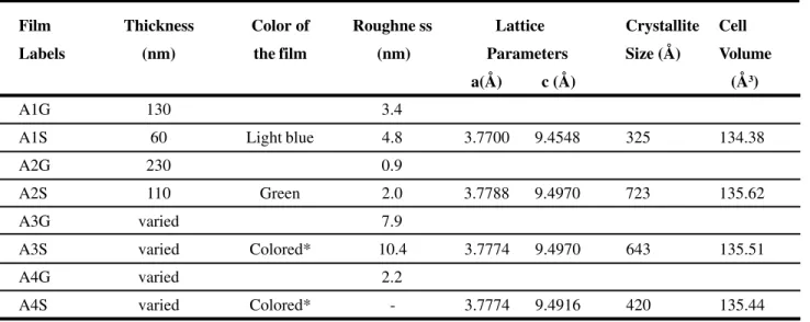
Film Thickness Color of Roughne ss Lattice Crystallite Cell
Labels (nm) the film (nm) Parameters Size (Å) Volume
a(Å) c (Å) (Å3)
A1G 130 3.4
A1S 60 Light blue 4.8 3.7700 9.4548 325 134.38
A2G 230 0.9
A2S 110 Green 2.0 3.7788 9.4970 723 135.62
A3G varied 7.9
A3S varied Colored* 10.4 3.7774 9.4970 643 135.51
A4G varied 2.2
A4S varied Colored* - 3.7774 9.4916 420 135.44
(*) Colored means that the films have more than just one color.
Table III - Physical characterization results of TiO2thin films. Each pair of thin film samples (A1G-A1S and A2G-A2S) was obtained from the same deposition run (same conditions) but using different substrates; G stands for glass and S for silicon(100), as shown in Table II.
The structural properties of the deposited films were studied by X-ray diffraction, and the measurements were carried out with a Siemens D5000 diffractometer with CuKαradiation. The geometry
of the diffractometer was the same for all samples (grazing incidence
diffraction - incidence angle = 2o, step time = 7s, step scan = 0.007o,
2θ = 20 – 50o, U = 40 kV and I = 40 mA. The surface morphology of
the TiO2 thin films was analyzed by scanning electron microscopy
using a Zeiss DSM940A microscope. Film thickness was determined by analyzing the cross section images. More detailed information on morphology and roughness was obtained by atomic force microscopy (AFM) (Digital Instruments Multi-Mode Nanoscope III A).
RESULTS AND DISCUSSION
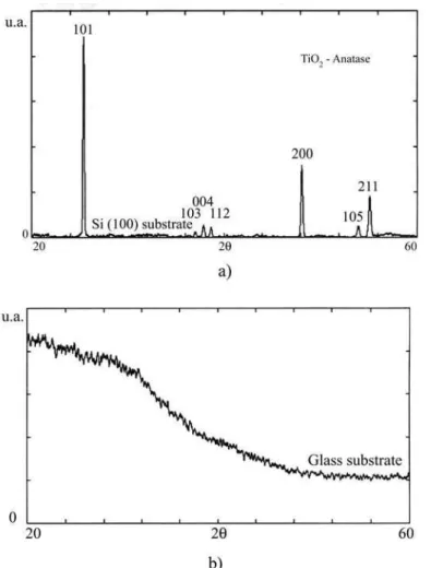
The results show that the amorphous glass structure lead to titania in the amorphous phase. Otherwise, the crystalline silicon substrate, induced the anatase crystal structure for the film.
Figure 2: X-ray diffraction patterns of TiO2 thin films deposited on
glass and on Si (100) substrates, under the same conditions.
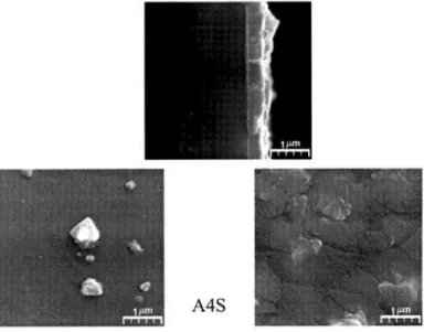
Figure 3: SEM micrographs of the cross section of TiO2 thin films
deposited on different substrates, under the same conditions: a) glass and b) Si(100).
patterns, the structures are different, showing the influence of the nature of the substrate in each case. Fig. 2 also shows that the films deposited on Si (100) present a polycrystalline structure with the anatase phase. The films grown on glass, on the other hand, do not show crystalline structure, preserving their amorphous character.
The nature of the substrate, crystalline or amorphous, provides different degrees of packing and, consequently, different stages of density and thickness in the morphological structure of the obtained films [11]. This may be attributed to the fact that the mobility of the atoms on the substrate surface, which is responsible for the degree and type of nucleation on the substrate, depends on its nature.
The morphological analyses were of key importance to choose the substrates and bath precursors temperature. The collection of SEM micrographs presented in Fig. 3 shows surface and cross section views for the obtained TiO2 thin films. In Table II are listed the obtained films nomenclature.
Comparing the micrograph studies for A1 (S and G) with the A3 (S and G), growth using substrate temperature TS = 400 oC and
TS = 500 oC, respectively, it was observed that the A6G thin film
presents a distinct structure than other films. This special feature has already been observed in thin films obtained by the microwave growth technique [12]. For the A3S film, on the other hand, it was observed that the growth occurred in order to form plane plates with low adherence. Analyzing both A1S and A1G films, one can observe that these films present a homogeneous surface, with no
denditric or plate-form arrangements and uniform thickness. On the contrary, for the growth of A3 films, the determination of the thickness was not possible due to morphology irregularities. These results indicate that TS, the optimum temperature of the substrate for deposition of TiO2 films using the built apparatus is 400 oC.
A comparison of the results of A1(S and G) with the A4(S and G) growth in the bath temperature (TB) of 90 oC and 120 oC, respectively,
was done. These temperatures are thoroughly related to the partial pressure of the organomettalic compound, and the higher is the temperature, the vapor partial pressure is so high that the deposition is inadequate, leading to a non-homogeneous film. Hence, it is possible to conclude that the temperature of 90 oC favors the growth of clean
and more homogeneous films, since for films grown at 120 oC, A4
films, agglomerates are formed in the film surface.
In order to establish the chemical composition of the observed agglomerates, a chemical element mapping for the A4G film was also performed using the energy dispersive X-ray electron spectroscopy (EDS), as can be observed in Fig. 9. The elements found in such agglomerates are Au, from the recovering, Si, Na and Ca.These elements are present in the composition of the substrate and the occurrence of Na indicates a possible migration from the substrate surface to the film at this temperature.
After these analyses, it was established that the best temperature conditions were substrate temperature TS=400 oC and bath
Figure 5: AFM surface morphology of TiO2 thin films deposited on different substrates, under the same conditions: A1G and A2G, glass (amorphous) and A1S and A2S, Si(100) (crystalline).
Figure 4: Sample A4S surface EDX analyses, exhibiting TiO2
precipitation.
study the influence of the deposition time. The results, shown in Fig. 3, present just an increase in the thickness of the film. One can observe that the films deposited on the glass substrates are thicker than those grown on the Si (100) under the same conditions. It is also possible to observe a variation of color patterns with the increase of thickness, as shown in Table III. This effect of color variation is more evident for TiO2 films grown on Si (100) substrates; it could also be observed
on the glass ones, fact already reported elsewhere [12].
The films were visible at naked eye, once their color change, observed by reflection. TiO2 layers on glass showed different colors
(see Table III). These colored films were well red. The layer homogeneity was also visible, due to the interference phenomenon, also previously reported [13].
Studies of Atomic Force Microscopy were also performed to investigate the morphology of the films. In Fig. 5 it is possible to inspect an exemple of the surface structure and roughness listed in Table III. The data shows different crystallization patterns for both Si (100) and glass substrates. While the films grown on glass were composed by poorly defined grains, the films on Si (100) presented grain formations, in agreement with XRD data. It is necessary to point out that XRD experiments yields long and medium range order analysis, and on the contrary, the AFM is able to detect short range order. In our opinion, the AFM images of thin films on glass substrates here reported are just exhibiting the initial stage of crystallization, not detectable by X-ray diffraction analysis. Besides, observing the data presented in Table III, one can notice that the film roughness on glass substrates was always lower than those presented for the Si (100). This seems to confirm our results, since the roughness of the glass substrate (0,92 nm) is higher than that of Si (100), 0.20 nm.
The roughness values indicate the good quality and homogeneity of the films, showing that the increase of the deposition time leads to a decrease in the roughness, as reported for SnO2 films obtained
using the Pechini method [14].
crystalline phase, or oppositely, the deposition over a random structure of those products leads to an amorphous specimen. Not just the crystal structure of the substrate, but also its chemical bonding affects the growth of the film, conditioned to the energy competition between the volume and the interface, and furthermore, to the growth kinetics, that is dependent on substrate temperature (ST) and deposition rate (DR).
CONCLUSIONS
It was possible to obtain good quality thin films of TiO2 with acceptable homogeneity, adherent, speculating and with minor roughness using a simple and non-expensive equipment.
The films showed a strong dependence of the kind of substrate on the structural characteristics, and consequently to a variation of optical properties. The results suggested that the obtained film thickness is directly related to the deposition time.
Through the analysis of the films grown under different conditions, it was chosen the temperature of 90 oC for the
organometallic bath and 400 oC for the substrate temperature. Using
these conditions, it was possible to obtain crystalline thin films using Si (100) substrates and amorphous thin films using glass substrates.
ACKNOWLEDGEMENTS
The authors gratefully acknowledge the financial support of the Brazilian financing agencies Fundação de Amparo à Pesquisa do Estado de São Paulo (FAPESP), Conselho Nacional de Desenvolvimento Científico e Tecnológico (CNPq), Grupo de Pesquisa de Excelência (PRONEX) and Coordenação de
Aperfeiçoamento de Pessoal de Nível Superior (CAPES).
REFERENCES
[1] Y. Gao, S. Thevuthasan, D. E. McCready, M. Engelhard, J. Cryst. Growth 212 (2000) 178.
[2] D. R. Burgess, P. A. M. Hotsenpiller, T. J. Anderson, J. L. Hohman, J. Cryst. Growth 166 (1996) 763.
[3] Y. Gao, K. L. Merkle, H. L. M. Chang, T. J. Zhang, D. J. Lam, J. Mater. Res.6 (11) (1991) 2417.
[4] H. S. Yoon, S. K. Kim, H. S. Im, Bull. Korean Chem. Soc. 18 (1997) 641.
[5] P. A. M. Hotsenpiller, G. A. Wilson, A. Roshko, J. B. Rothman, G. S Rohrer, J. Cryst. Growth 166 (1996) 779.
[6] P. A. M. Hotsenpiller, A. Roshko, J. B. Lowekamp, G. S Rohrer, J. Cryst. Growth174 (1997) 424.
[7] D. Mardare, G. I. Rusi, Mater. Sci. & Eng.B75 (2000) 68. [8] S. M. Tracey, S. N. B. Hodgson, A. K. Ray, Z. Ghassemlooy, J. Mater. Proc. Technol. 77 (1998) 86.
[9] A. Bendavid, P. J. Martin, A. Jamting, H. Takikawa, Thin Sol. Films355-356 (1999) 6.
[10] D. Mergel, D. Buschendorf, S. Eggert, R. Grammes, B. Samset, Thin Sol. Films 371 (2000) 218.
[11] J. Sabate, M. A. Anderson, H. Kikkawa, Q. Xu, S. Cervera-March, C. G.Hill Jr., J.Catal.134 (1992) 36.
[12] E. Vigil, L. Saadoun, J. A. Ayllón, X. Domènech, I. Zumeta, R. Rodríguez-Clemente, Thin Sol. Films 365 (2000) 12.
[13] S. M. Zanetti, E. R. Leite, E. Longo, J. A. Varela, J. Mater. Res.14 (1999) 1026.