Structural Characterization of ZnTe Grown by Atomic-Layer-Deposition Regime on GaAs
and GaSb (100) Oriented Substrates
1Roberto Saúl Castillo-Ojedaa, Joel Díaz-Reyesb*, Miguel Galván-Arellanoc, Francisco de Anda-Salazard,
Jorge Indalecio Contreras-Rascone, María de la Cruz Peralta-Clarab, Julieta Salomé Veloz-Rendónb
Received: February 29, 2016; Revised: October 21, 2016; Accepted: November 21, 2016
This work presents the characterization of ZnTe nanolayers grown on GaAs and GaSb (100) substrates by the Atomic Layer Deposition (ALD) regime. Under certain conditions, the alternating exposition of a substrate surface to the element vapours makes possible the growth of atomic layers in a reactor where the atmosphere is high-purity hydrogen. ZnTe was grown simultaneously on GaAs
and GaSb at the same run, allowing, a comparison between the efects produced by the supericial processes due to the diferent used substrates, thereby eliminating possible unintended changes of
growth parameters. Nanolayers on GaSb maintained their shiny appearance even at temperatures near 420°C. It was found that for exposure times below 2.5 s there was not growth on GaAs, while for GaSb
the shortest time was 1.5 s at 385°C. By HRXRD the peak corresponding to (004) difraction plane of ZnTe was identiied and investigated, the FWHM resulted very wide (600-800 arcsec) indicating
a highly distorted lattice mainly due to mosaicity. Raman scattering shows the peak corresponding to LO-ZnTe, which is weak and slightly shifted in comparison with the reported for the bulk ZnTe at 210 cm-1. Additionally, the measurements suggest that the crystalline quality have a dependence with
the growth temperature.
Keywords: Atomic Layer Deposition, nanolayers, X-ray difraction, Raman scattering
1 Article presented and selected from “The XXIV International Materials
Research Congress (IMRC) 2015”. Symposium 5B “Structural and Chemical Characterization of Metals, Alloys and Compounds”. Cancun, Mexico August 16-20, 2015.
* e-mail: [email protected]
1. Introduction
Nowadays, most of the modern electronic devices are based on the growth of nanometric layers, strained or not; superlattices, quantum wells, optical modulators, hot-electron transistors, are only a few examples of the wide
ield of application of them1-4. Among the most successful
semiconductor materials for the radiation detection, ZnTe
has excellent optical properties as its quantum eiciency.
ZnTe has proved to be a very successful material for the radiation detection in its bulk form although is a promising material for radiation detection in its nanolayers form5,6.
The layer by layer growth regime can be implemented by a
precise control of the precursor lows in systems as CVD, MOCVD, MBE, Radical-Enhanced ALD7,10. Normally, this is
done by exposing the substrate, in an alternating way to the
vapour of each one of the constituent elements of the layer, followed by a purge or dead period between exposures in order to evacuate adequately the growth chamber. An important characteristic of ALD is its self-regulated nature7-10. In this
work are presented the results obtained of the growth and characterization of ZnTe epitaxial layers on GaSb and GaAs by ALD regime under an ambiance of high purity hydrogen at atmospheric pressure.
2. Experimental Procedure
The growth system used in the experiments is depicted in Figure 1, which has a horizontal geometry; the body of the reactor is made of a quartz tube while the suceptor is made of high purity graphite. The experiments were performed using
a high purity Pd-Ag difused hydrogen low of 300 ml/min.
aUniversidad Politécnica de Pachuca, Carretera Pachuca-Cd. Sahagún Km. 20, Rancho Luna,
Ex-Hacienda de Sta. Bárbara, Zempoala, Hidalgo, 43830, México
bCentro de Investigación en Biotecnología Aplicada, Instituto Politécnico Nacional, Ex-Hacienda de
San Molino, Km 1.5 de la Carretera Estatal Santa Inés Tecuexcomac-Tepetitla, Tepetitla de Lardizábal, Tlaxcala, 90700, México
cDepartamento de Ingeniería Eléctrica, Sección de Electrónica del Estado Sólido, Centro de Investigación
y de Estudios Avanzados, Instituto Politécnico Nacional, Apartado Postal 14-740, City of México, 07000, México
dInstituto de Investigación en Comunicación Óptica, Universidad Autónoma de San Luis Potosí, Ave.
Karakorum 1470, Lomas 4ª Sección. Álvaro Obregón, 64, San Luis Potosí, 78210, México
layers, ellipsometric measurements were performed using a Gaertner ellipsometer L117 with and He-Ne laser with
λ = 632.8 nm, varying the incident angles and obtaining
the extinction parameters. Raman scattering experiments were performed at room temperature using the red laser at
λ=6328 Å at normal incidence. The light was focused in a circular spot of 6 μm diameter on the sample using a 50×
(numerical aperture 0.9) microscope objective. The nominal
laser power used in these measurements was 20 mW. Care
was taken to avoid the heating of the sample inadvertently to the point of changing its Raman spectrum. Scattered light was analysed using a Dilor micro-Raman spectrometer, with
a holographic notch ilter made by Kaiser Optical System, Inc. (model superNotch-Plus), a 256×1024-pixel CCD used
as detector, and two interchangeable gratings (600 and 1800
g/mm). Typical spectrum acquisition time was limited to 60 s to minimize the sample heating efects discussed above.
Absolute spectral feature position calibration to better than 0.5 cm-1 was performed using the observed position of Si,
which is shifted by 521.2 cm-1 from the excitation line.
2.1. ZnTe Growth Procedure
The experiments were carried out in a wide temperature range but ZnTe layers with a shiny surface could be grown only at temperatures between 370 and 400°C on both GaSb and GaAs substrates. In the case of the GaAs substrates, for temperatures above 400°C, the layer surface deteriorated and showed a milky aspect but on GaSb the layer surfaces kept their shiny appearance even at temperatures near 420°C. In other set of experiments, the exposure times to Zn and Te vapours were explored, in order to determine the shortest exposure times that could be used to grow the ZnTe layers in the ALD regime. It was found that for exposure times below 2.5 s there was not growth on the GaAs substrates, while in the case of GaSb the shortest time was found to
be 1.5 s for 385°C. This diference in the exposure times indicates that the associated growth kinetic is diferent for
GaSb and GaAs substrates. In addition, these times are not determined by the transport of the reactants on the growth surfaces. For subsequent experiments 3 s was taken as the exposure time for samples growth, and 3 s for the interruption time, as other authors have reported14. The ZnTe layer
thicknesses were evaluated by ellipsometric measurements. The normalized results are summarized in Figure 2, in this
one, the measured layers were grown using diferent numbers of exposition cycles in an interval since 300 to 900. In igure
the horizontal scale corresponds to the growth temperatures used in the experiments.
The mean value of the thickness per cycle was around 0.3 nm that is the value corresponding to a monolayer of ZnTe. This indicates that the growth regime is the known as Atomic Layer Deposition (ALD). As was pointed out, the growth regime of ALD allows having a very good control on
Figure 1: Details of suceptor used for growing the samples. 1)
Elemental source, 2) quartz container, 3) slide strip holder, 4) GaAs
and GaSb substrates, 5) purge hole.
The substrates are exposed alternatively to the precursor vapours by sliding a graphite rule containing them. The elemental precursor vapours arrive on the substrate surface from little quartz tubes where are contained. In this way
both of them, the anion lux and the cation lux saturate the
growth surface one after the other taking advantage of the self-regulated process characteristic11-13. All, the graphite
suceptor, substrates and precursor sources were maintained at the same temperature. The graphite rule with the substrates is coupled to a step motor controlled by a computer program. This motor is located outside of the growth chamber. The computer program allows sequencing the layer growth and provides the desired exposure time.
The substrates preparation was as usually; degreased with organic solvents, oxide elimination using HCl followed by a chemical polishing. In the case of the GaAs substrates the used etching solution was H2SO4:H2O2:H2O, 5:1:1, while in the GaSb case was used a solution based in tartaric acid,
hydroluoric acid and hydrogen peroxide11. After the chemical
etching, the substrates were rinsed in deionized water and dried by blowing nitrogen on their surfaces. As next step, the substrates were introduced into the growth chamber and were placed side by side on a graphite rule. In order to guarantee the same growth conditions on both GaSb and GaAs substrates, the two substrates were used simultaneously at the same growth run. This was accomplished cutting
rectangular substrates of 0.5 cm×1.0 cm and placed side by side to form a 1.0 cm×1.0 cm substrate. In this way were
eliminated possible factors introduced by nonintentional variation in the growth processes assuring the same growth conditions for the deposited layers on both substrates and allowing the direct comparison between the grown layers on GaSb and GaAs substrates.
In order to study the structural characteristics of the epitaxial
layers grown with diferent temperatures and thicknesses, high-resolution X-ray difraction (HRXRD) measurements were performed. All the X-ray difractograms were acquired using a Philips Analytical difractometer. For scanning the used parameters were: Cu Kα1 line with wavelength of 1.5406
Å, Δλ/λ=2×10-4, and 0.10 sec as time per step, the relection
Figure 2: Thicknesses of the grown epitaxial layers as function of growth temperature.
the layer thickness, due to the close dependence of the inal
thickness on the total number of growth cycles performed.
3. ZnTe X-ray Difraction Measurements
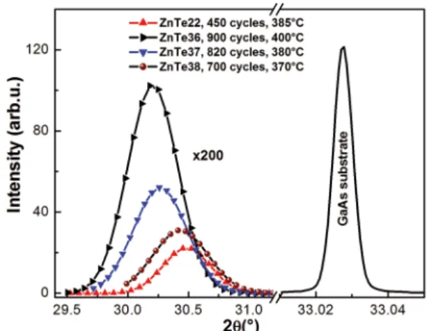
Figure 3 shows the X-ray difractograms of the grown
samples, as a result of the HRXRD measurements, it can be
observed, the peak corresponding to the (004) difraction plane of ZnTe layer, which was identiied and investigated. The thin peak near 33° corresponds to the (004) difraction plane
from the GaAs substrate and it was used as reference for the ZnTe layer peaks position adjustment and their comparison. The wide peaks to the left of the same one corresponding
to the (004) difraction plane from the deposited layers, their vertical intensities were ampliied by 200 times due
to the weaknesses of these peaks as a consequence of the
thin thickness involved on the difraction. The full width at half maximum (FWHM) of the difraction peaks are very
wide (600-800 arcsec) indicating a highly distorted lattice mainly due to mosaicity15. In addition, in this igure can be
observed that the intensity of the peaks increases with the
thickness of the layers. Moreover, as the layer thickness
increases, the peak position moves away from the peak corresponding to GaAs substrate towards the position that must have the corresponding to the ZnTe in its bulk form.
This efect can be attributed to the relaxation of the layers
and the increase of dislocation defects in the interface in addition for highly dislocated layers the peak position is related with the mean distortion of the lattice and with the dislocation density generated in the relaxation process16. For
the samples showed in Figure 3 the calculated thicknesses were between 135 to 270 nm.
In the case of ZnTe layers grown on GaSb substrate was not possible to resolve clearly the ZnTe peak from the one corresponding to GaSb substrate. This can be attributed as consequence of the small lattice mismatch between the ZnTe layer and the GaSb substrate. The lattice constants of the two
Figure 3: X-ray difractograms of ZnTe grown on GaAs, peak
position shift is related with the growth temperature and with the layer thickness.
materials are very close, aGaSb= 6.0959 Å and aZnTe= 6.1034
Å. In addition, the interface defects and the nanometric
thicknesses of the ZnTe layers are factors related to the
full width at half maximum of the difraction peak17,18. The
above described is shown in Figure 4, where is presented a
X-ray difraction curve of a typical 125 nm thick ZnTe layer,
obtained performing 410 growth cycles on GaSb substrate. Additionally, the peak position of the layer is closer to the peak of substrate, considering the critical thickness of 275 nm on (100) GaSb reported by other authors17. As a result of
the deconvolution treatment of the experimental curve can be observed the peak corresponding to the ZnTe layer near the
dominant peak corresponding to the (004) difraction plane of
the GaSb substrate. Compared with the GaSb substrate peak can be note a large peak width of the layer and its weakness is evident due to the nanometric thickness combined with
the misit dislocation density among other factors.
4. ZnTe Characterization by Raman
Spectroscopy
Back scattering geometry has been used to record the Raman spectra of the (100) GaSb and GaAs substrates, which are shown in Figure 5. GaSb Raman spectrum which presents a dominant band that is associated to longitudinal optical phonon (LO) frequency of GaSb observed at 237 cm−1, and another which is related to metallic tellurium observed at 274 cm−1 that was found experimentally. The weak shoulder on the low-frequency side of the GaSb-LO band at 229 cm−1 is the GaSb-TO mode, in principle forbidden in this experimental geometry. Its weak intensity in our Raman spectrum indicates that the crystalline quality of the Te-doped GaSb substrate is very good. Similarly, to GaAs substrate, which only shows a Raman peak at 293 cm-1 that is
Figure 4: ZnTe and GaSb deconvoluted (004) peak. The substrate
and layer peaks are diicult to resolve.
Figure 5: Raman spectra of the substrates used in the growth of
thin ilms of ZnTe.
had been thin ilm growth on diferent used substrates. Figure
5 shows the Raman spectra of GaAs and GaSb substrates, which have as dominant vibrational mode Longitudinal Optical (LO). And Raman spectroscopy measurements grown layers were performed for assessing the quality of the ZnTe. The obtained results are shown in Figure 6. As was mentioned above the measurements were carried out at room temperature on samples (001) oriented with normal
incidence. The layers presented in igure were grown on GaSb
and GaAs substrates. The transversal optical (TO) mode is
forbidden in the experimental measurement coniguration
geometry for (001) substrate orientation, it becomes active by the breakdown of the selection rules in the backscattering
coniguration. This breakdown is attributed to the generation of structural defects as misit dislocation in the layer-substrate
interface, inhomogeneity and other crystallinity problems
originated from compositional luctuations and by elastic
scattering from ionized impurities. The peak observed at 208 to 211 cm-1 is associated to the ZnTe longitudinal optical
(LO) phonon peak19-26, details of this peak are presented in
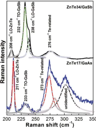
Figure 6: ZnTe Raman measurements of samples grown on GaSb. LO-ZnTe peak shows a dependence with the growth temperature as is illustrated in Table 1.
Figure 7: Raman spectra of ZnTe samples grown with diferent
Figure 7. The peaks at 274 to 290 cm-1 are composed by
the TO-GaAs and LO-GaAs vibrational modes, originated from the GaAs substrate, because of the penetration depth of laser light is larger than the ZnTe layer thickness and reaches the substrate, so the Raman spectra exhibit peaks related to the substrate characteristics. The peak near 231 cm-1 is the
corresponding to the GaSb substrate and is composed of the TO-GaSb and LO-GaSb in 238 cm-1. In addition, the peak
corresponding to LO-ZnTe shows weakness and a slightly displacement in comparison with the reported for the bulk ZnTe at 210 cm-1 19-26, possibly due to the layers stress and
the nanometric thickness of these layers, as has been reported by other authors21.
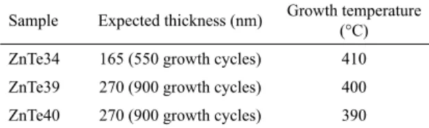
As can be observed in Table 1, the samples labelled as
ZnTe40, ZnTe39 and ZnTe34 were grown with diferent
temperatures, comparing the peak near 210 cm-1 the sample
grown with the lower temperature shows a more intense and thin peak corresponding to the LO-ZnTe, see Figure 6. This is indicative of a dependence of the growth temperature with
the crystalline quality of samples. This efect of temperature
with the Raman spectra of ZnTe can be associated with
the misit dislocation increase in the interface due to the
dependence of dislocation density with the temperature. The samples presented in Figure 6 were grown on GaSb with the growth temperature and thickness presented in Table 1.
As can be observed in Figures 6 and 7 the corresponding peaks coming from the substrate have the TO-GaSb peak,
which must be forbidden for the experimental coniguration
used in the measuring due to the substrate orientation (100). In this case, it can be associated with the crystalline quality of the substrate. The appearance of this peak is indicative
Table 1: ZnTe growth conditions used for samples presented in Figure 6 grown on GaSb
Sample Expected thickness (nm) Growth temperature (°C)
ZnTe34 165 (550 growth cycles) 410
ZnTe39 270 (900 growth cycles) 400
ZnTe40 270 (900 growth cycles) 390
of crystalline defects in the substrate, which is propagating to the layer grown of ZnTe.
5. Conclusions
In this work is reported the successfully growth of ZnTe on both GaAs and GaSb substrates by the Atomic Layer Deposition regime as was shown from the thickness
measurements performed by ellipsometry. X-ray difraction shown a dependence of the (004) difraction peak position
with temperature and with the sample thickness which can be attributed to the lattice relaxation produced by the increase
of interface defects. In addition, Raman characterization shown that the obtained samples presented a large density of
crystalline defects possible dominated by misit dislocation,
additionally the samples grown at low temperature shown better Raman spectra (LO-ZnTe dominant) indicating in this way a crystalline quality dependence with the growth temperature.
6. References
1. Göbel EO, Ploog K. Fabrication and optical properties of
semiconductor quantum wells and superlattices. Progress in Quantum Electronics.1990;14(4):289-356.
2. Ritala M, Leskelä M. Atomic layer epitaxy - a valuable tool
for nanotechnology? Nanotechnology. 1999;10(1):19-24.
3. Shan CX, Fan XW, Zhang JY, Zhang ZZ, Ma JG, Lu YM, et al.
Growth and characterization of ZnCdTe-ZnTe quantum wells on ZnO coated Si substrate by metalorganic chemical vapor deposition. Journal of Crystal Growth. 2001;233(4):795-798.
4. Im H, Wittenberg NJ, Lindquist NC, Oh SH. Atomic layer
deposition (ALD): A versatile technique for plasmonics and nanobiotechnology. Journal of Materials Research. 2012;27(4):663-671.
5. Ruzin A, Nemirovsky Y. Methodology for evaluation of
mobility-lifetime product by spectroscopy measurements in CdZnTe spectrometers. Journal of Applied Physics. 1997;82(9):4166-4171.
6. Nemirovsky Y, Ruzin A, Asa G, Gorelik J. Study of the charge collection eiciency of CdZnTe radiation detectors. Journal of Electronic Materials. 1996;25(8):1221-1231.
7. George SM. Atomic Layer Deposition: An Overview. Chemical
Reviews. 2010;110(1):111-131.
8. Hsu CT. Epitaxial growth of II-VI compound semiconductors
by atomic layer epitaxy. Thin Solid Films. 1998;335(1-2):284-291.
9. Lee W, Kim S, Song J, Ko H, Yao T, Cho YR, et al. Molecular beam epitaxy of GaSb on ZnTe/GaAs: Inluence of the chemical
composition of ZnTe surface. Applied Surface Science. 2008;254(23):7728-7732.
10. Ahonen M, Pessa M, Suntola T. A study of ZnTe ilms grown
on glass substrates using an atomic layer evaporation method.
Thin Solid Films. 1980;65(3):301-307.
11. Berishev IE, de Anda F, Mishournyi VA, Olvera J, Ilyinskaya
ND, Vasilyev VI. H2O2:HF:C4O6H6 (Tartaric acid): H2O
Etching System for Chemical Polishing of GaSb. Journal of
the Electrochemical Society. 1995;142(10):L189-L191.
12. Hartmann JM, Charleux M, Mariette H, Rouvière JL. Atomic layer epitaxy of CdTe, MgTe, and MnTe; growth of CdTe/ MnTe tilted superlattices on vicinal surfaces. Applied Surface
Science. 1997;112:142-147.
14. Larramendi EM, Purón E, Hernández LC, Sánchez M, De Roux S, de Melo O, et al. Atomic layer epitaxy of ZnTe by
isothermal closed space sublimation. Journal of Crystal Growth. 2001;223(4):447-449.
15. Kim BJ, Wang JF, Ishikawa Y, Park YG, Sindo D, Abe S, et al. Strain in the HWE-grown ZnTe/(100) GaAs hetero-interface. Journal of Crystal Growth. 2002;235(1-4):201-206.
16. Kaganer VM, Köhler R, Schmidbauer M, Opitz R, Jenichen B. X-ray difraction peaks due to misit dislocations in heteroepitaxial
structures. Physical Review B. 1997;55(3):1793-1810.
17. Chai J, Noriega OC, Dedigama A, Kim JJ, Savage AA, Doyle K, et al. Determination of Critical Thickness for Epitaxial ZnTe Layers Grown by Molecular Beam Epitaxy on (211)B
and (100) GaSb Substrates. Journal of Electronic Materials. 2013;42(11):3090-3096.
18. Birkholz M. Thin Film Analysis by X-Ray Scattering. Weinheim: Wiley; 2005. 378 pages.
19. Levy M, Amir N, Khanin E, Nemirovsky Y, Beserman R. Characterization of CdTe substrates and MOCVD Cd1-xZnxTe
epilayers. Journal of Crystal Growth. 1999;197(3):626-629.
20. Zielony E, Placzek-Popko E, Henrykowki A, Gumienny Z, Kamyczek P, Jacak J, et al. Laser irradiation efects on the CdTe/ZnTe quantum dot structure studied by Raman and AFM
spectroscopy. Journal of Applied Physics. 2012;112(6):063520.
21. Vinogradov VS, Karczewski G, Kucherenko IV, Mel’Nik NN,
Fernandez P. Raman spectra of structures with CdTe-, ZnTe-, and CdSe-based quantum dots and their relation to the fabrication technology. Physics of the Solid State. 2008;50(1):164-167.
22. Olego DJ, Raccah PM, Faurie JP. Compositional dependence of
the Raman frequencies and line shapes of Cd1-xZnxTe determined
with ilms grown by molecular-beam epitaxy. Physical Review
B. 1986;33(6):3819-3822.
23. Su YK, Gan KJ, Hwang JS, Tyan SL. Raman spectra of Si-
implanted GaSb. Journal of Applied Physics. 1990;68(11):5584-5587.
24. Milekhin A, Werninghaus T, Zahn DRT, Yanovskii Y,
Preobrazhenskii V, Semyagin B, et al. Raman and infrared spectroscopical investigation of the optical vibrational modes
in GaSb/AlSb superlattices. The European Physical Journal B - Condensed Matter and Complex Systems. 1998;6(3):295-299.
25. Chen XK, Wiersma R, Wang CX, Pitts OJ, Dale C, Bolognesi
CR, et al. Local vibrational modes of carbon in GaSb and GaAsSb. Applied Physics Letters. 2002;80(11):1942-1944.
26. Ersching K, Campos CEM, de Lima JC, Grandi TA, Souza SM, da Silva DL, et al. X-ray difraction, Raman, and photoacoustic