Thyristorized Rectifier Bridge
Controlled Through a PSoC
Eduardo M. Vicente*, Paula dos Santos*, Carlos A. Gallo**, Robson L. Moreno*, Enio R. Ribeiro* *Grupo de Microeletrônica - IESTI, Universidade Federal de Itajubá. Itajubá-MG, Brasil
**Faculdade de Engenharia Mecânica, Universidade Federal de Uberlândia. Uberlândia-MG, Brasil
[email protected], [email protected], [email protected], [email protected], [email protected]
Abstract—This work presents the design and implementation of a control system for a thyristorized rectifier bridge held by PSoC (Programmable System-on-Chip), which is able to maintain the output current of the circuit in a predetermined reference supporting changes in input voltage, as well as changes in load. Using the PSoC – an integrated circuit that has programmable analog and digital resources - it is possible to reduce the external circuitry. The project built with the PSoC, compared with a conventional implementation, is smaller and has lower costs. Another important aspect is related to the decrease in energy consumption due to the use of fewer components. The rectifier and its control system were designed and simulated. Additionally, a prototype was built and the tests proved the feasibility of using PSoC.
I. INTRODUCTION
One needs existing in the electrical systems is the conversion of an alternating voltage into a DC voltage. For this task it is common to use rectifier bridges, which produce a variable output voltage. The control system of a rectifier bridge uses different integrated circuits (ICs), as well as auxiliary circuits, to convert the signals from each part of the circuit. The system developed by [1], among some applications of the rectifier bridge, uses the MC6809 microprocessor to perform the control of a three-phase rectifier bridge, which feeds a DC motor. Additionally, some discrete components and integrated circuits are used, such as the timer VIA6522, which is responsible for generating the trigger pulse of the thyristors.
The reference [2] presents a dual converter feeding a DC motor. The control system of the dual converter uses a smaller number of external circuits, since a great number of functions are performed by the 68HC11 microcontroller. However, the trigger pulse generation system depends on extra components such as: counter, comparator and demultiplexer. Finally, in [3], is seen a control system for a three-phase induction motor. Although it used a circuit suitable for the driving of controllable devices, such as thyristors and triacs, the TCA780, resulting in a considerable decrease in the number of external components, the control system is accomplished through analog PI controllers.
The search for cost reduction due to the decrease or the efficient use of raw materials leads the researches for the production of optimized systems (fewer components, lower power consumption, etc.), as seen in [4], [5] and [6].
Following this trend, the System-on-Chip - integrated circuits that incorporate different features, configurable and programmable, in an integrated circuit - are available on the market. Thus, this work presents the implementation of a thyristorized rectifier with constant current output, using a System-on-Chip, i.e. the PSoC (Programmable System-on-Chip developed and produced by Cypress Semiconductor Corp.). The use of PSoC reduces the amount of discrete circuitry of the conversion system and consequently has a lower system cost, flexibility (change of functions), among other features.
The system developed in this study took into account the circuits used in applications previously mentioned, [1], [2] and [3], noting the advantages and disadvantages of each approach in order to evaluate the parts of the circuit that could be integrated in the PSoC, thus reducing the total number of external circuits. In this project, the PSoC was chosen because it provides useful resources for the intended application, such as timers, which will be used to generate the trigger pulses for the thyristors, analog to digital (A/D) converters used in converting the output current, amplifiers and filters, responsible for the signal conditioning. Another important aspect of this choice was the lack of articles involving this technology in power electronics.
II. PSOCMICROCONTROLLER
The integrated circuits System-on-Chip (SoC) are devices that have several resources, whether analog or digital, in just one chip. This type of circuit is desirable, since the integration of components into a single chip, allows the reduction of external interference such as from trails connections and electromagnetic effects. This makes the SoC more reliable and less prone to errors [7]. With SoC is possible to design a system, with minimal use of external connections and other chips [8]. Moreover, as resources are integrated, it is possible to achieve greater operating speed, system reliability and robustness, allowing its use in certain applications.
The features available in the SoC devices can generate conditions appropriate to the needs of a particular project, providing even the addition of new features to the application, as they are available on the device.
configure not only the code to be executed, but also the resources you want to use and the pins which they are connected, this flexibility increases the number of applications, [9] and [10].
III. RECTIFIER BRIDGE CONTROLLED BY THE PSOC In power electronics one of the needs is the conversion of AC voltage to DC voltage. One of the devices used in energy conversion is the rectifier bridge, which converts an alternating voltage into a DC voltage, and has been used with new approaches, as seen in [11]. The average output voltage (VLmed), of a thyristorized rectifier bridge, is obtained with (1), where Vo is the RMS input voltage and α the firing angle.
(
1 cos)
.. . 45 ,
0 + α
= o
Lmed V
V (1)
There are two ways to characterize the firing angle, through the comparison of the control voltage Vc and a reference voltage VREF, with a saw-tooth or a cosine wave characteristic. Through the second method of comparison it is possible to obtain a linear relationship between the firing angle and the average voltage output, which results in a better response of the converter. Because of this characteristic, this type of comparison was implemented on this work. The relationship between the control voltage and the firing angle can be seen in (2), where VM is the cosine maximum reference voltage.
. 1 . 9 ,
0 ⎟⎟⎠
⎞ ⎜⎜ ⎝ ⎛
− =
M c
o Lmed
V V V
V
(2)
The block diagram of the developed system is presented in Fig. 1, and each block will be explained in the next section.
A. Auxiliary Circuits
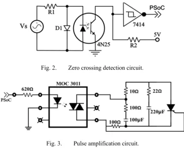
As the circuit responsible for the detection of zero crossing, the phototransistor 4N25 was used, it works similarly to the circuit seen in [1]. It is simple to implement and requires only two resistors and a diode, to adjust the input and output of the IC. Its circuit is shown in Fig. 2. To drive the thyristors, the MOC3011 driver was used. It is an optocoupler with triac output. This component is similar to the device seen in [1], and needs few resistors and capacitors in circuits of input and output. Fig. 3 shows how the driver is connected to each thyristor of the rectifier bridge.
Fig. 1. Circuit block diagram.
Fig. 2. Zero crossing detection circuit.
Fig. 3. Pulse amplification circuit.
To measure the output current the Hall sensor, LA-25NP, was chosen due to its simplicity and ease of connection with other systems. The device was configured in a manner that the conversion ratio was set to 1:200, e.g., a measured current of 5 amperes corresponds to a current of 25 milliamperes at the output of the sensor.
B. Developed Circuits
This section presents the circuits implemented with the PSoC, substituting the external circuitry. The pulses that will trigger the thyristors will be generated by the PSoC through its internal timers, as illustrated in Fig. 4. The timers outputs are connected through AND functions to the output of a PWM block with a frequency of 10 kHz. This strategy is widely used in Power Electronics, as seen in [12], and aims to reduce the power dissipated in the control device.
To get the average voltage at the Hall sensor output, which is proportional to the output current of the circuit, an internal low-pass filter was used, as shown in Fig. 5. With this feature, the need for external capacitors or an external circuit consisting of operational amplifiers, as used by [2], was eliminated.
Fig. 4. Timer block diagram.
simplifying adjustments, reducing the interferences and the final cost of the project.
Fig. 5. Connecting the low-pass filter with the current sensor.
To calculate the control voltage Vc, which will be used later
to obtain the firing angle α, a PI controller for the current control loop, was used. This choice took into account the results obtained in the applications examined. The control is implemented on the PSoC, allowing rapid adjustment of parameters, when compared with analog control circuits and due to the resources of the microcontroller, such as MAC (Multiply Accumulate 32-bit), the controller calculus are performed in a small amount of time. There is, in Fig. 6, an overview of the internal blocks of the PSoC.
In the PSoC Designer image, at left, there are the digital blocks, which implement: the zero crossing detection, the timers, the 10 kHz oscillator and the PWM used in the interrupt generation of the A/D converter. On the right side, there are the analog blocks: the A/D converter and the low-pass filter. The availability of the analog and digital resources in the microcontroller depends on the chosen family. In this application the CY8C29466-24PXI PSoC chip was used. It has 16 digital blocks and 12 analog blocks available, which enables its use in several circuits.
(a) (b)
Fig. 6. Control circuit design in the PSoC Designer: (a) digital blocks, (b) analog blocks.
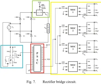
In Fig. 7 there is the thyristorized rectifier bridge circuit, controlled through the PSoC. In the lower left corner, there is
the circuit responsible for the zero crossing detection. In the upper center, the Hall sensor, which will provide the reference output current. At right, the trigger circuit, and in the lower center, the PSoC.
Fig. 7. Rectifier bridge circuit.
With the circuit diagram, the control system was developed, and the gains were adjusted to obtain the appropriate response to this type of circuit.
IV. CONTROL SYSTEM DEVELOPMENT
To select the gains of PI controller and demonstrate its operation through a computer program, the rectifier bridge and circuits used for measuring the output current, were modeled with the objective of creating an appropriate computational model, [13]. The block diagram of the control system can be seen in Fig. 8.
Fig. 8. Control system block diagram.
The transfer function, after some calculus, is presented by (3).
⎟ ⎠ ⎞ ⎜ ⎝ ⎛ + ⎟⎟ ⎠ ⎞ ⎜⎜ ⎝ ⎛ ⎟⎟ ⎠ ⎞ ⎜⎜ ⎝ ⎛ ⎟⎟ ⎠ ⎞ ⎜⎜ ⎝ ⎛ − ⎟⎟ ⎠ ⎞ ⎜⎜ ⎝ ⎛ + + ⎟⎟ ⎠ ⎞ ⎜⎜ ⎝ ⎛ ⎟⎟ ⎠ ⎞ ⎜⎜ ⎝ ⎛ ⎟⎟ ⎠ ⎞ ⎜⎜ ⎝ ⎛ − ⎟⎟ ⎠ ⎞ ⎜⎜ ⎝ ⎛ + = sRC R V V V s K s K R V V V s K s K s I s I L M C o i p L M C o i p REF 1 1 1 . 1 . . 9 , 0 . . 1 1 . 1 . . 9 , 0 . . ) ( ) ( (3)
Performing the multiplications, and considering that:
VM = 5 V; Vo = 127 V; VC = 2 V; RL = 10 Ω;
It follows (4).
⎟ ⎟ ⎠ ⎞ ⎜
⎜ ⎝ ⎛
+ − +
⎟ ⎟ ⎠ ⎞ ⎜
⎜ ⎝ ⎛
+ + + +
⎟ ⎟ ⎠ ⎞ ⎜
⎜ ⎝
⎛ −
+
⎟ ⎟ ⎠ ⎞ ⎜
⎜ ⎝
⎛ +
+ =
50 343
1036 2590
50 343
227 343 1554
343 1036 2590 343
343 1554
) (
) (
2 2
p p i
p i p
p p i
p i p
REF
K K K
K K K s s
K K K K
K K s s
s I
s I
(4)
For the proportional and integral gains, a comparison is made between the modeled system and the characteristic equation of a 2nd order system. The gains were: 0.33 (proportional gain) and 5.8 (integral gain). Through the simulation of the control function, adjustments were made in the selected gains in order to get a better response from the controller. Thus, the values chosen for the proportional and integral gains were:
12 , 1 = p
K
, Ki=35,4
Setting up the constants of the controller, an electrical circuit was built and simulated computationally. The simplified circuit is shown in Fig. 9.
Fig. 9. Simplified circuit of the controlled rectifier bridge.
V. RESULTS A. Simulation results
The control system was evaluated and its response to load and input voltage variations is presented below. The first situation is the response of the circuit to an input step at startup. The load resistance was 20 Ω and the reference current was set at 2 amperes. The waveform of the average current output, during a startup transient, is shown in Fig. 10. For this step, the settling time was 1.1 seconds and the overshoot 30%.
Fig. 10. Input step response of the control system (0,4A/div, 0,2s/div).
In the following essay, the reference current was set at 2 amperes and the load varied 50%. The output waveform can be seen in Fig. 11. The response time was 800 milliseconds and the overshoot 30%. In the subsequent test a variation in input voltage was performed. The load was maintained at 20 Ω
and the reference current in 2 amperes. By varying the input voltage from 75 to 100%, the response time was 600 milliseconds and the overshoot 10%. The waveform of the average current output can be seen in Fig. 12.
Fig. 11. Average current output for a negative change of 50% in the load (0,4A/div, 0,2s/div).
Fig. 12. Average current output for a variation in input voltage from 75 to 100% (0,4A/div, 0,2s/div).
The results presented for the control system were satisfactory and demonstrate the operation of the designed PI controller.
B. Experimental Results
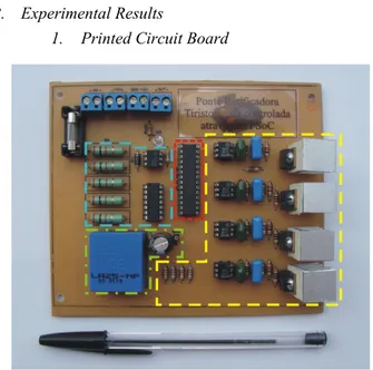
1. Printed Circuit Board
The final PCB is presented in Fig. 13. At left, the circuit responsible for the zero crossing detection. In the lower left corner, the circuit that performs the measurement of the output current. On the right, the trigger circuit, along with the bridge thyristors, which are coupled to heat sinks. At the center, the PSoC. The dimensions of the PCB are 12x14 cm. The load circuit was made by 4 incandescent lamps, three 100 watts lamps and one of 200 watts, with a total load of 500 watts.
2. Constant input voltage and variable load
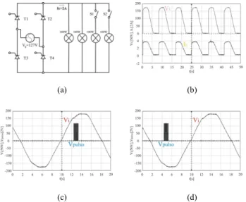
In the tests presented below, the input voltage was kept constant at 127 volts, the reference current in 2 amperes and the load was varied in order to demonstrate the operation of the control system. A lamp of 200 watts and another one of 100 watts together with two 100 watts lamps were used, connected by S1 and S2, as shown in the circuit of Fig. 14.
(a) (b)
(c) (d)
Fig. 14. Test with a load of 300 W: (a) circuit, (b) voltage (VL) and
current (IL) in load, (c) input voltage (Vi) and trigger pulses at thyristors
T1 and T4 (Vpulso), (d) input voltage (Vi) and trigger pulses at thyristors T2 and T3 (Vpulso).
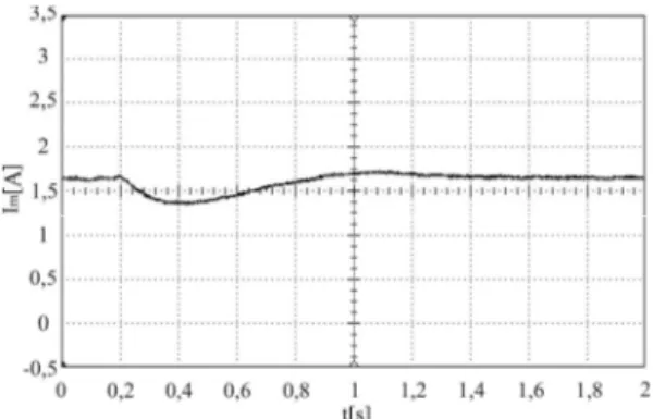
Another important aspect is the time spent until the output of the circuit stabilizes after a change in the load. In Figs. 15 and 16 it is possible to observe the output current of the circuit and the elapsed time until it becomes stable again, during the load change from 300 to 500 watts (switches S1 and S2 closing simultaneously). In Fig. 15 is presented the current output, directly measured in the load. In Fig. 16, it is shown the average current that is measured with the internal low-pass filter of the PSoC.
In the first test the response time were satisfactory when compared with the results obtained in other applications [1], [2] and [3], considering that every second it is possible to perform 120 iterations (one every 8.33 milliseconds). The output stabilized at around 1.2 seconds and presented an overshoot of 46%. The peak current in the load, which is observed in Fig. 15, is caused by harmonic currents in the load and is a characteristic of the thyristor rectifier bridges, according to [12]. The current output of the low-pass filter,
Fig. 16, shows different values from the reference established. In the graph, the measured value is approximately 1.7 amperes, while the reference is 2 amperes. This difference is justified, in part due to the use of internal references, by the PSoC, to convert the signal. Another justification is related to the finite number of α values, in which the control system will select the value that best matches the benchmark set.
Fig. 15. Current output in load during the change from 300 to 500 W (2A/div, 0,1s/div).
Fig. 16. Average current output in the PSoC during load change from 300 to 500 W (0,5A/div, 0,2s/div).
From the previous situation, load of 500 watts, both switches, S1 and S2, were opened simultaneously. The corresponding waveforms of this situation can be observed in Figs. 17 and 18. The current variation was lower, comparing with the previous essay, and were around 23% and the accommodation time 800 milliseconds.
Fig. 18. Average current output in the PSoC during load change from 500 to 300 W (0,5A/div, 0,2s/div).
3. Constant load and variable input voltage
In the tests presented below, the output current was set again in 2 amperes, the load was kept constant at 300 watts, and the input voltage was modified through a variable transformer. These tests were performed to demonstrate the ability of the control system to respond to variations in the input voltage. In the first essay, the input voltage varied from 100 to 75%, resulting in the waveform of Fig. 19. The first try-out has a response time of 1 second and a slight variation in the current, about 5%. In the second situation, varying the input voltage from 75 to 100%, Fig. 20, the response time was approximately 900 milliseconds and the overshoot 8%.
Fig. 19. Average current output during the PSoC variation of input voltage from 100 to 75% (0,5A/div, 0,2s/div).
Fig. 20. Average current output during the PSoC variation of input voltage from 75 to 100% (0,5A/div, 0,2s/div).
VI. CONCLUSION
The design and implementation of a control system for a thyristorized rectifier bridge was developed in this paper. In the first part, the control system was simulated, which came to confirm the operation of the designed system and parameters used. In the next moment, the system was implemented with real components and the PSoC microcontroller. The results were satisfactory and similar to those seen in computer simulation. Another advantage to be deployed was the considerable decrease in external circuitry, especially when compared to solutions provided by [1], [2] and [3]. Compared to these cases, it was obtained a 40% reduction of the external circuitry. In addition to the benefits of circuit dimension reduction, there is the lowest energy consumption, increased power density and higher efficiency of the structure, which allows using this type of solution in a large number of applications. It should also be noted the ease of modification of the project, as the circuits integrated in the PSoC, can be changed or reconfigured dynamically.
ACKNOWLEDGMENT
Authors would like to thank CAPES and the PRPPG – UNIFEI for the financial support at this work. The author MsC. Eduardo M. Vicente thanks Cypress Semiconductors for the support and Dr. Carlos A. Gallo is thankful to INCT-EIE.
REFERENCES
[1] Sinzato, M. G. (1991). Implementação de um controle de velocidade e corrente para motor de corrente contínua. 1991. 158 f. Dissertação (Mestrado em Ciências em Engenharia Elétrica) - Escola Federal de Engenharia de Itajubá, Itajubá. [2] Vermaas, L. L. G.; Lenarth, G. L.; Valberto, F. V. (1996). Implementação de um
Equipamento Didático para Conversor Dual baseado em Microcontrolador. In: XI Congresso Brasileiro de Automática - XI CBA, 1996.
[3] Pereira, C. A. G. (2003). Otimização de reguladores para acionamento controlado de motores de indução alimentados por intermédio de inversor de corrente com comutação natural. 2003. 115 f. Dissertação (Mestrado em Ciências em Engenharia Elétrica) - Universidade Federal de Itajubá, Itajubá. [4] Li, Q.M. (2003). A low-cost configurable PWM controller using programmable
system-on-chip. Power Electronics Specialist Conference, 2003. PESC '03. IEEE 34th Annual Vol. 3, pp. 1169 - 1174.
[5] Muresan, M.; Chindris, G. (2005). PSoC dual sensor for pressure and temperature using bipolar junction effects.Electronics Technology: Meeting the Challenges of Electronics Technology Progress, 2005. 28th International Spring Seminar on, pp. 62 – 66.
[6] Tong, C. C.; Tsai Y. J.; Li S. F.; Lin J. Y.; Ho M. H.; Lin Y. H. (2008). PSoC implementing vehicle auxiliary vacuum brake system with Kalman filter. IEEE Asia Pacific Conference on Circuits and Systems. APCCAS 2008. pp. 77 - 81. [7] Júnior, V. C. (2005). Tecnologia SoC e o microcontrolador PSoC
(Programmable System on Chip). Revista Integração, São Paulo, Ano XI, n.° 42, p. 251-257.
[8] Hock, B. C. L. (2004). PSoC optical sensor game pad - Project Number C2930. In: CIRCUIT CELLAR PSOC HIGH INTEGRATION CHALLENGE. [9] Nicolosi, D. E. C.; Santos, R. C. (2006). Microcontrolador PSoC: uma nova
tecnologia, uma nova tendência. 1. ed. São Paulo: Érica, 414p.
[10] Doboli, A. N.; Currie, E. H. (2007). Introduction to Mixed-Signal, Embedded Design. 1. ed. San Jose, California: Cypress Semiconductor Corporation, 473p. [11] Buddingh, P.; St. Mars, J.R. (2000). New life for old thyristor power rectifiers
using contemporary digital control, IEEE Transactions on Industry Applications, Vol. 36, Issue: 5. pp. 1449 - 1454.
[12] Barbi, Ivo. (2000). Eletrônica de Potência. 3. ed. Florianópolis: Edição do Autor. [13] Phillips, C. L.; Nagle JR., H. T. (1984). Digital control system analysis