Brazilian Journal of Physics, vol. 29, no. 4, December, 1999 771
Band Crossing Evidence in PbSnTe Observed by
Optical Transmission Measurements
S. O. Ferreira
1, E. Abramof
2, P. Motisuke
2, P. H. O. Rappl
2, H. Closs
2,
A. Y. Ueta
2, C. Boschetti
2, and I. N. Bandeira
2,
1: Dep. Fsica, Universidade Federal de Vicosa, 36571-000, Vicosa, MG, Brazil
2: Instituto Nacional de Pesquisas Espaciais, C.P. 515 - 12201-970 S~ao Jose dos Campos, SP, Brazil
ReceivedFebruary 8,1999
Using high quality epitaxial layers, we have obtained direct evidence of the band inversion in the Pb1,xSnxTe system. The samples, covering the whole composition range, were grown by
molecular beam epitaxy on (111)BaF2substrates. A minimumin the resistivity as a function
of temperature was observed for all samples with Sn composition 0:35x0:70. In the
same samples and at the same temperature, temperature dependent optical transmission measurements have revealed a change in signal of the energy gap temperature derivative, a direct evidence of the band inversion. However, the temperature for which the inversion occurs is not the one expected by the band inversion model. This discrepancy is supposed to be due to the Burstein-Moss shift caused by the relatively high hole concentration observed in these samples.
I Introduction
Lead-tin telluride is a narrow gap semiconductor which have been investigated for many years and applied mainly in the fabrication of infrared (3-14 m) photo detectors and diode lasers [1,2]. The growth of epi-taxial layers and multi-layer structures like superlat-tices and multi-quantum wells of narrow gap IV ,V I
compounds by molecular beam epitaxy (MBE) has im-proved the basic research of quantum eects in these materials [3,4]. New interesting research possibilities were opened by alloying the binary and also ternary lead salts with rare-earth elements (mainly Eu and Y b) to produce compounds with higher energy gaps and their respective multi-layer heterostructures [5]. Re-cently, the growth of lead salts on silicon substrates us-ing uoride buer layers, in order to obtain the mono-lithic integration of lead salt detector arrays with silicon read-out circuits, has also received much attention [6,7]. According to the band inversion (BI) model [8], the Pb1,xSnxTe energy gap (Eg) initially decreases as the
Sn composition increases, and vanishes for an inter-mediate alloy composition. Further increasing the Sn composition, the energy gap starts to increase, with the
band edge states inverted, up to the SnTe value. The Sn composition for which the band inversion should occur varies from x 0:35 to x 0:70 as the
tem-perature increases from 4 to 300 K. However, it is very dicult to determine the band edge structure near and beyond the band inversion region, since only high car-rier concentration samples can be obtained due to the deviation from the stoichiometry [9]. The energy gap of Pb1,xSnxTe has been experimentally determined only
for the range x < 0:25. The Burstein-Moss shift, caused by the high hole concentration, which is observed in the samples with higher tin composition (x > 0:30), imposes diculties in the determination of the \real" gap by optical-absorption measurements [10,11]. In this composition range, the only available Eg experimental
data has been determined by tunneling measurements in Al,Al
2O3
,SnTe structures [12]. The "real" E g
of pure SnTe (p 10
20cm,3) is 0.18 eV [12], while
the \optical energy gap" was found to be near 0.5 eV [10,11].
magne-772 S.O.Ferreiraet al
toplasma method. They have observed much heavier eective masses in these doped samples as compared with the values expected for the undoped Pb1,xSnxTe
and an energy gap which does not go to zero. In their conclusions, they state that it is dicult to say if this behavior is essential for PbSnTe or a result of the In doping. Although the BI model is widely accepted, di-rect observation for the Pb1,xSnxTe system has not
been achieved yet, mainly due to the lack of good qual-ity samples with x > 0:30 and with low carrier concen-tration.
II Experimental
Recently, we have reported on the growth of high quality PbSnTe samples, covering the whole compo-sition range [14]. The PbSnTe layers were grown on (111)BaF2 substrates by molecular beam epitaxy
us-ing solid PbTe and SnTe sources. The growth tem-perature was between 250 and 300 oC and the nal
thickness was about 4m. The samples were charac-terized by high resolution x-ray diraction, tempera-ture dependent resistivity, Hall mobility and infrared transmission. The lms grown using stoichiometric PbTe and SnTe sources have shown a hole concentra-tion between p = 110
17cm,3, for Pb
0:85Sn0:15Te, to
p = 210
19cm,3, for SnTe. This p value, observed
for SnTe, is at least one order of magnitude lower than the one previously reported in the literature. Such a lower carrier concentration increases the hall mobilities of all samples and makes easier their optical character-ization. Details about the electrical characterization of these layers have been published elsewhere [15].
Another important feature is a well dened mini-mum in the temperature dependent resistivity and a corresponding maximum in the mobility of all samples with 0:35x0:70, as can be observed in the Fig. 1
for two typical PbSnTe layers.
According to the BI model, this composition range corresponds to that where band crossing should occur. Since this behavior can be observed only for the samples in the band crossing range, it seems that this minimum in the resistivity is related to the band inversion. For the samples in this range, the energy gap should rst reduce with decreasing temperature, as it happens for PbTe. But after the band inversion it should increase with further decrease in temperature, the behavior of SnTe. This change in the signal of the energy gap tem-perature coecient (dEg=dT), would be the reason for
the behavior observed in the resistivity and mobility.
Figure 1. Resistivity as a function of temperature for two typicalPbSnTe samples in the band inversion region.
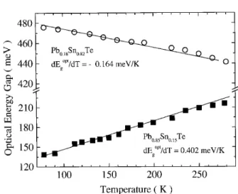
Figure 2. Optical energy gap as a function of temperature for twoPbSnTe samples outside the BI region.
To clarify this point, the temperature dependence of the energy gap for all samples, mainly that covering the BI region, was measured. The energy gap was deter-mined from the transmission spectra, which were mea-sured using a Fourier transform infrared spectrometer in the range from 4500 to 800 cm,1 for temperatures
Brazilian Journal of Physics, vol. 29, no. 4, December, 1999 773
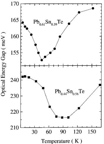
Figure 3. Optical energy gap as a function of temperature for two typical PbSnTe samples in the BI region. The lines
are guides to the eye.
As expected, the energy gap increases with tem-perature, for the sample with x = 0:15, while it de-creases, for the sample with x = 0:82. But, in contrast to model, the absolute value of the temperature coef-cients (dEg=dT) were very dierent. This occurs
be-cause the Egvalue taken from the transmission spectra
is the \optical energy gap" (Eop
g ), which takes into
ac-count the Burstein-Moss (BM) shift, due to the band lling. For the Pb0:85Sn0:15Te layer the BM shift is
negligible (p = 310
17cm,3) and the measured values
of Eg and dEg=dT are the ones expected from the
lit-erature [16]. On the other hand, for the sample with x = 0:82 (p = 110
19cm,3), the BM shift is 230
meV at 80 K, and dEop
g =dT is a combination of the
changes in the energy gap and in the position of the Fermi level. Preliminary calculations of the absorption coecient, using a model proposed by Anderson [17], which takes the BM shift into account, explain the re-duction in dEop
g =dT observed for samples with high hole
concentration.
The temperature dependence of Eop
g for the samples
in the band inversion region is completely dierent, as
shown Fig. 3.
The optical energy gap rst reduces, reaches a min-imum, and than starts to increase. Again, due to the relatively high carrier concentration of the samples, the temperature coecient of Eop
g is much smaller than the
expected value of dEg=dT. The temperature where this
minimumin Eop
g occurs coincides with the temperature
of minimumresistivity for all samples in the band inver-sion region. Fig. 4 plots the temperature of minimum resistivity and minimum Eop
g as a function of Sn
con-tent for all our MBE samples, together with the band crossing temperature predicted from the BI model.
Figure 4. Temperatures of minimum resistivity () and of dE
op g
=dT = 0 (). The solid line is the band crossing
tem-perature calculated from the BI model.
III Conclusion
The Burstein-Moss shift in the PbSnTe system, due to the high hole concentration, produces a strong change in the temperature dependence and absolute value of the optical energy gap. The change in signal of dEop
g =dT, for Pb
1,xSnxTe samples with 0:35
x
774 S.O.Ferreiraet al
Acknolegments
This work has been partially supported by \Con-selho Nacional de Desenvolvimento Cientco e Tec-nologico-CNPq" and \Fundac~ao de Amparo A Pesquisa do Estado de S~ao Paulo-FAPESP".
References
1. H. Holloway and J.N. Walpole, Prog. Crystal Growth Charact. 2, 49 (1979).
2. H. Preier, Appl. Phys. 20, 189 (1979).
3. D.L. Partin, in: Semiconductors and Semimetals, Vol. 33, Ed. T.P. Pearsall (Academic Press, New York, 1991) p. 311.
4. G. Springholz, G. Ihninger, G. Bauer, M.M. Olver, J.Z. Pastalan, S. Romaine and B.B. Goldberg, Appl. Phys. Lett. 63, 2908 (1993).
5. G. Springholz and G. Bauer, J. Crystal Growth
144, 157 (1994).
6. C. Boschetti, P.H.O. Rappl, A.Y. Ueta and I.N. Bandeira, Infrared Phys. 34, 281 (1993).
7. H. Zogg, A. Fach, C. Maissen, J. Masek and S. Blunier, Optical Engineering33, 1440 (1994).
8. J. Dimmock, I. Melngailis and A.J. Strauss, Phys. Rev. Lett. 16, 1193 (1966).
9. T. C. Harman, J. Nonmetals,1, 183 (1973).
10. E.G. Bylander, J.R. Dixon, H.R. Riedl and R.B. Schoolar, Phys. Rev. 138, A873 (1965).
11. R.B. Schoolar, H.R. Riedl and J.R. Dixon, Solid State Commun.4, 423 (1966).
12. L. Esaki and P.J. Stiles, Phys. Rev. Lett. 16,
1108 (1966).
13. S. Takaoka, S. Shimomura, H. Takahashi and K. Murase, Phys. Rev. B,40, 5642 (1989)
14. P.H.O. Rappl, H. Closs, S.O. Ferreira, E. Abramof, C. Boschetti, P. Motisuke, A.Y. Ueta and I.N. Bandeira, J. Cryst. Growth, 191, 466
(1998).
15. E. Abramof, S.O. Ferreira, P.H.O. Rappl, H. Closs And I.N. Bandeira, J. Appl. Phys., 82, 2405
(1997).