DEPARTMENT OF INFORMATION SCIENCE AND TECHNOLOGY
MONTE-CARLO SIMULATION OF AN OPTICAL DIFFERENTIAL PHASE-SHIFT KEYING COMMUNICATION SYSTEM WITH DIRECT DETECTION IMPAIRED BY
IN-BAND CROSSTALK
Dissertation presented in partial fulfillment of the Requirements for the Masters Degree on Telecommunications and Information Science
By
Genádio João Faria Martins
Supervisors:
Dr. Luís Cancela, Assistant Professor, ISCTE-IUL
Dr. João Rebola, Assistant Professor, ISCTE-IUL
Copyright © 2012 All rights reserved
I
Acknowledgments
First of all, I would like to thank my supervisors Prof. João Rebola and Prof. Luís Cancela for all their support throughout this work and their availability and patience in all my doubts and questions. I would like to thank Instituto de Telecomunicações (IT) for providing me material, access to their installations and for the monthly scholarship.
I would like to thank also my family for their support, love and encouragement, which was fundamental for the realization of this dissertation, particularly to my cousin Tonita. A special thanks to my girlfriend Sara Rocha for all her patience and support.
Finally, I would like to thank all my friends, particularly Rui Batalha, João Conduto and Catarina Cruz for all their support and help mainly during the computer simulations. Thank you all!
Lisbon, 2012 Genádio Martins
III
Resumo
O renovado interesse nas comunicações ópticas com modulação de fase diferencial DPSK (differential phase-shift keying) provém do facto de esta superar o formato convencional de modulação de intensidade, OOK (on-off keying) em certos aspectos, tais como, sensibilidade do receptor, robustez às limitações da transmissão e tolerância às flutuações da potência do sinal. O crescimento exponencial do tráfego de dados e as vantagens do DPSK levam à necessidade da sua utilização no contexto das redes ópticas, sendo uma das principais limitações físicas das redes ópticas, o crosstalk.
O crosstalk homódino incoerente, devido ao isolamento imperfeito dos componentes ópticos utilizados nos nós da rede óptica, tem sido identificado como uma das maiores limitações existentes no nível físico das redes ópticas.
Esta dissertação apresenta um estudo do impacto do ruído de emissão espontânea amplificada, gerado pela amplificação óptica do sinal, e do crosstalk no desempenho de um sistema de comunicação óptico DPSK com detecção directa e assumindo um receptor balanceado.
O desempenho do sistema é avaliado usando uma simulação estocástica baseada no método de Monte Carlo e comparado com o desempenho obtido a partir de formulações analíticas. Diferentes combinações de filtros ópticos e eléctricos são considerados no receptor óptico DPSK. A influência de imperfeições do receptor óptico DPSK no desempenho é também estudada. Investiga-se também a influência do nível de potência do sinal de crosstalk, o atraso entre o sinal original e o sinal de crosstalk e diferentes sequências de bits no sinal de crosstalk DPSK no desempenho do sistema de comunicação óptico.
Palavras-chave: Sistemas de comunicação óptica, simulação de Monte Carlo, modulação de fase diferencial, crosstalk homódino incoerente e ruído de emissão espontânea amplificada.
V
Abstract
The renewed interest in optical communications on the differential phase-shift keying (DPSK) modulation format comes from the fact that it outperforms the conventional format on-off keying (OOK), in such aspects, such as receiver sensitivity, robustness to transmission impairments and tolerance to signal power fluctuations. The exponential growth of data traffic and the DPSK advantages over OOK lead to its use on the optical networks environment, where physical limitations, such as crosstalk, may impair significantly the network performance.
In-band crosstalk, due to the imperfect isolation of optical components used in the optical network nodes, has been identified as one of the most severe physical layer limitation in optical transparent network.
This dissertation proposes to study the impact of amplified spontaneous emission noise, generated by the signal optical amplification, and of in-band crosstalk in the performance of an optical DPSK communication system with direct detection using a balanced receiver.
A stochastic simulation based on the Monte Carlo method is used to evaluate the system performance and comparisons with the results obtained using theoretical works are also performed. Different combinations of optical and electrical filters at the optical DPSK receiver are considered. The influence of DPSK receiver imperfections on the system performance is also studied. The influence of the crosstalk level, the delay between the original and the crosstalk signal and different bits sequence on the DPSK crosstalk signal on the system performance is also investigated.
Keywords: Optical communication system, Monte Carlo simulation, differential phase-shift keying, in-band crosstalk and amplified spontaneous emission noise.
VII
Index
1. Introduction ... 1
1.1. Motivations ... 1
1.2. Objectives and dissertation organization ... 2
2. Theoretical concepts ... 5
2.1. Introduction ... 5
2.2. Transmitter description ... 6
2.3. Receiver description ... 9
2.3.1. Optical amplifier, polarizer and optical filter ... 9
2.3.2. MZDI and dual photodetector ... 10
2.3.3. Electrical filter and decision circuit ... 13
2.4. Implementation of the Monte Carlo simulator ... 14
2.4.1. Signals simulation ... 14
2.4.2. Monte Carlo simulation ... 16
2.4.3. The Monte Carlo simulation flowchart ... 17
3. Optical DPSK communication system impaired by ASE noise ... 21
3.1. Introduction ... 21 3.2. Filters characterization ... 22 3.2.1. Ideal filter ... 22 3.2.2. Gaussian filter ... 22 3.2.3. Lorentzian filter ... 23 3.2.4. Integrator filter ... 23 3.2.5. RC filter ... 24
3.3. Validation of the Monte Carlo simulation... 26
3.4. Performance evaluation for different optical and electrical filters combinations ... 32
VIII
3.4.2. Gaussian optical filter and integrator electrical filter ... 33
3.4.3. Lorentzian optical filter and integrator electrical filter ... 35
3.4.4. Gaussian optical filter and Gaussian electrical filter ... 36
3.4.5. Gaussian optical filter and RC electrical filter ... 37
3.4.6. Comparison of the different filters combinations ... 39
3.5. Impact of the DPSK receiver imperfections ... 40
3.5.1. Validation of the MC simulation ... 41
3.5.2. Performance evaluation for different optical and electrical filter combinations .... 42
3.6. Conclusions ... 48
4. Optical DPSK communication system impaired by in-band crosstalk ... 51
4.1. Introduction ... 51
4.2. In-band crosstalk model ... 52
4.3. Implementation of the random phase noise ... 54
4.4. Validation of the Monte Carlo simulation... 57
4.5. Performance evaluation ... 61
4.5.1. Delay between the original signal and the crosstalk signal ... 62
4.5.2. Different bits sequences on the DPSK crosstalk signal ... 64
4.5.3. Receiver imperfections ... 67
4.6. Conclusions ... 69
5. Conclusions and future work ... 71
5.1. Future work ... 73
IX
List of Figures
Figure 2.1 - Schematic block diagram of an optical DPSK communication system. ... 5
Figure 2.2 - Principle of phase modulation using a MZM (adapted from Fig. 3 of [6]). ... 6
Figure 2.3 –NRZ signal and the phase of the DPSK signal. ... 7
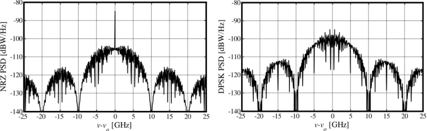
Figure 2.4 – PSDs of NRZ (left) and DPSK (right) signals. ... 8
Figure 2.5 – PSDs of signals 2(t) at constructive port (left) and 1(t) at destructive port (right). ... 11
Figure 2.6 – Photocurrents, i1(t), i2(t) and i(t). ... 13
Figure 2.7 – Signal at the decision circuit output. ... 14
Figure 2.8 – Simulated time vector. ... 15
Figure 2.9 – Simulated frequency vector. ... 15
Figure 2.10 – Block diagram of the Monte Carlo simulation. ... 16
Figure 2.11 – Flowchart of the MC simulation for a back-to-back configuration. ... 18
Figure 3.1 – Ideal filter transfer function for BoTb = 100. ... 22
Figure 3.2 – Electrical integrator filter transfer function for BeTb = 1. ... 24
Figure 3.3 – Amplitude response of the Gaussian and Lorentzian optical filters. ... 24
Figure 3.4 – Amplitude response of the Gaussian and RC electrical filters. ... 25
Figure 3.5 – Group delay of the RC filter for different electrical filter –3 bandwidths. ... 26
Figure 3.6 – BEP as a function of the optical signal power, for the ideal OF and the integrator EF combination, considering BoTb = 1, 10 and 100... 27
Figure 3.7 – BEP as a function of the optical signal power, for the ideal OF and the integrator EF combination considering smaller normalized optical filter bandwidths. ... 28
Figure 3.8 – PDF of the decision variable, for the ideal OF and the integrator EF combination, considering an optical signal power with –47 dBm and BoTb = 1, 5 and 10. ... 28
Figure 3.9 – Eye diagram at the decision circuit input for the ideal OF and the integrator EF combination, considering BoTb equal to 1 (left), 5 (middle) and 10 (right). ... 29
Figure 3.10 – BEP as a function of BoTb, considering the ideal OF and the integrator EF combination tested for different number of bits. ... 30
Figure 3.11 – BEP as a function of BoTb, for the ideal OF and the integrator EF combination, considering different optical signal powers. ... 32
X
Figure 3.12 – PDF of the decision variable, for an ideal OF and an integrator EF combination, considering an optical signal power with –47 dBm for BoTb = 1, 1.1, 1.2, 1.3, 1.4 and 1.5. ... 33
Figure 3.13 – BEP as a function of BoTb, for the Gaussian OF and the integrator EF
combination, considering different optical signal powers. ... 34 Figure 3.14 – Eye diagram at the decision circuit input for the Gaussian OF and the integrator EF combination, considering BoTb equal to 1 (left), 2 (middle) and 10 (right). ... 35
Figure 3.15 – BEP as a function of BoTb, for the Lorentzian OF and the integrator EF
combination, considering different optical signal powers. ... 35 Figure 3.16 – PDF of the decision variable, for the Lorentzian OF and the integrator EF combination, considering an optical power with –47dBm for BoTb = 1, 2, 5 and 10. ... 36
Figure 3.17 – BEP as a function of BoTb, for the Gaussian OF and the Gaussian EF
combination, considering different optical signal powers. ... 37 Figure 3.18 – BEP as a function of BoTb, for a Gaussian OF and a RC EF combination,
considering different optical signal powers. ... 38 Figure 3.19 – Eye diagram at the decision circuit input, considering a Gaussian OF and a RC EF combination, an optical signal power equal to –47 dBm, for BoTb = 2 (left) and BoTb = 10
(right). ... 38 Figure 3.20 – BEP estimates as a function of BoTb, for a Gaussian OF and a RC EF
combination, considering different signal optical powers and for a sampling time equal to half bit period. ... 39 Figure 3.21 – BEP as function of the optical signal power for BoTb = 5, considering different
filters combinations. ... 40 Figure 3.22 – BEP as a function of the responsivity imbalance for a matched optical filter and absence of electrical filter, considering different values of the interferometer detuning. ... 42 Figure 3.23 – Power penalty as a function of the responsivity imbalance for an ideal OF and integrator EF combination, considering different values of BoTb. ... 43
Figure 3.24 – Eye diagram at the decision circuit input for an ideal OF and integrator EF, considering K = 0 dB (left), K = 5 dB (middle) and K = 10 dB (right). ... 44 Figure 3.25 – PDFs of the decision variable, for an ideal OF and integrator EF, considering
K = 0 dB (red), K = 5 dB (blue) and K = 10 dB (green). ... 44
Figure 3.26 – Power penalty as a function of the responsivity imbalance for different values of
BoTb, considering a Lorentzian OF and integrator EF combination (left) and a Gaussian OF
XI Figure 3.27 – Power penalty as a function of the normalized interferometer detuning for an ideal OF and integrator EF combination, considering different values of BoTb. ... 46
Figure 3.28 – Eye diagram at the decision circuit input for an ideal OF and integrator EF, considering ∆f Tb = 0 (left), ∆f Tb = 0.04 (middle) and ∆f Tb = 0.08 (right). ... 47
Figure 3.29 – Power penalty as a function of the normalized interferometer detuning considering different values of BoTb, for a Lorentzian OF and integrator EF combination (left)
and for a Gaussian OF and a Gaussian EF combination (right). ... 48 Figure 4.1 – Schematic block diagram of an optical DPSK balanced receiver impaired by in-band crosstalk. ... 53 Figure 4.2 – Temporal evolution of the Brownian motion random phase noise, for two independent sample functions. ... 55 Figure 4.3 – PDF of random phase considering different temporal instants. ... 56 Figure 4.4 – PDF of the random phase noise difference. ... 57 Figure 4.5 – BEP as a function of the optical signal power, for an ideal OF and an integrator EF, considering BoTb = 1, 10 and 100 and the crosstalk level equal to –12 dB. ... 58
Figure 4.6 – BEP as a function of the crosstalk level, considering the ideal OF and the integrator EF combination (left) and the Gaussian OF and the RC EF combination (right), for different normalized optical filter bandwidths. ... 59 Figure 4.7 – Eye diagrams at the decision circuit input for the ideal OF and the integrator EF, for an optical signal power of –45 dBm, BoTb = 10 and considering a crosstalk level equal to
–30 dB (left), –20 dB (middle) and –12 dB (right). ... 60 Figure 4.8 – Power penalty as a function of the responsivity imbalance with different interferometer detunings, for the Gaussian OF and the Gaussian EF with a crosstalk level of –15 dB, considering a normalized optical filter bandwidth equal to 5. ... 61 Figure 4.9 – BEP as a function of the optical signal power, for an ideal OF and an integrator EF combination, a crosstalk level of –12 dB and a normalized optical filter bandwidth equal to 10 (left) and 100 (right), considering different crosstalk signal delays. ... 62 Figure 4.10 – BEP as a function of the delay between the crosstalk and the original signals, considering a Gaussian OF and a RC EF combination (left) and an ideal OF and an integrator EF combination (right), both for a crosstalk level of –12 dB and BoTb = 2. ... 63
Figure 4.11 – Eye diagram at the decision circuit input considering an ideal OF and an integrator EF combination, for three crosstalk signals delays equal to 0 (left), Tb/2 (middle)
XII
Figure 4.12 – BEP as a function of the crosstalk level, considering an ideal OF and an integrator EF combination with an optical signal power of –46 dBm (left) and a Gaussian OF and a RC EF combination with an optical signal power of –45 dBm (right), for different sequence of bits on the DPSK crosstalk signal, considering a normalized optical filter bandwidth equal to 2 and 10. ... 64 Figure 4.13 – Eye diagrams at the decision circuit input considering a Gaussian OF and a RC combination, for a random bits sequence on the DPSK crosstalk signal (left), an equal bits sequence (middle) and a negated bits sequence (right). ... 65 Figure 4.14 – PDFs of the decision variable, considering a Gaussian OF and a RC EF, for a random bits sequence on the DPSK crosstalk signal (blue), an equal bits sequence (red) and a negated bit sequence (green). ... 66 Figure 4.15 – BEP as a function of the responsivity imbalance (left) and of the interferometer detuning (right), for different crosstalk levels, considering a Gaussian OF and a Gaussian EF combination, a normalized optical filter bandwidth equal to 5 and an optical signal power of –45 dBm. ... 67 Figure 4.16 – PDF of the decision variable, considering responsivity imbalance (left) and of the interferometer detuning (right), for a crosstalk level of –12 dB, considering a Gaussian OF and a Gaussian EF combination, BoTb = 5 and an optical signal power of –40 dBm. ... 68
XIII
List of Tables
Table 3.1. Parameters of the simulated optical DPSK communication system impaired by ASE noise. ... 21 Table 3.2. The evolution of the BEP estimates and the simulation time with the increase of the number of errors, Ne, of the MC simulation. ... 31
Table 4.1. Parameters of the simulated optical DPSK communication system impaired by in-band crosstalk. ... 51
XIV
List of Acronyms
ASE Amplified Spontaneous Emission AWGN Additive White Gaussian Noise BEP Bit-Error Probability
CW Continuous Wave
DFT Discrete Fourier Transform DPSK Differential Phase-Shift Keying
DQPSK Differential Quadrature Phase-Shift Keying EDFA Erbium Doped Fiber Amplifier
EF Electrical Filter
FFT Fourier Fast Transform
IFFT Inverse Fourier Fast Transform ISI Inter-Symbol Interference MC Monte Carlo
MZDI Mach-Zehnder Delay Interferometer MZM Mach-Zehnder Modulator
NRZ Non-Return-to-Zero OA Optical Amplifier OF Optical Filter OOK On-Off Keying
OSNR Optical Signal-to-Noise Ratio PDF Probability Density Function PIN Positive Intrinsic Negative PM Phase Modulator
PSD Power Spectral Density PSK Phase-Shift-Keying
SOA Semicondutor Optical Amplifier WDM Wavelength Division Multiplexing
1
1. Introduction
1.1. Motivations
In the last few years, the data traffic in the communication networks had an exponential growth. Communication networks are undergoing dramatic changes due to increasing demands from users and also due to technological advances. All consumers have their own specific requirements on the networks in terms of bandwidth, quality of service and network resources. Optical technology has a key role to play enabling that optical networks can support these requirements [1].
The invention of the laser in 1958 and the subsequent demonstration of the optical fiber as a telecommunications transmission medium, in the 1960’s, brought a technology platform capable of supporting global communication demands for the 21st century and beyond [2]. In the 1970’s, a breakthrough occurred when the optical fibers losses were reduced to below 20 dB/km and, due to its advantages over the copper cables, such as, lower attenuation, broader bandwidth, reduced diameter and weight, and immunity to electromagnetic interference [3, chap. 1], these fibers began to replace coaxial cables as the transmission medium in the trunk systems of telecommunication systems [2]. The deployment of Internet in the mid-80’s, sparked a growth of data traffic on the network [2]. During these years, millions of kilometers of optical fiber were deployed world wide [4]. As a result, optical fibers became the dominant transmission medium in the telecommunication networks. In the 1990’s this capacity has been significantly increased due to the technology known as wavelength division multiplexing (WDM). The economic deployment of WDM was only possible due to the introduction of optical amplification with erbium-doped fiber amplifiers (EDFAs). The deployment of optical amplifiers and of WDM strongly contributed, respectively, to the increase of optical transmission reach and to the increase of the amount of traffic carried by an optical fiber. For these reasons, it is desirable for nodes to have switching add/drop capabilities at the optical level. This led to the development of optical add/drop multiplexers (OADMs) and optical cross connects (OXCs). Besides routing the optical paths, these components are also used to protect and restore the optical paths in case of failure, and enable the rapid reconfiguration of lightpaths [2].
1. Introduction
2
Current networks employ bit rates up to 100 Gbps and there are many reasons for believing that the bit rates will continue to increase [1]. However, the increase of the bit rate leads to more demanding requirements in the WDM systems design, due to enhancement of the dispersion effect (chromatic and polarization), of the nonlinear effects and of the crosstalk [3, chap. 3, 4 and 9]. Crosstalk due to the imperfect nature of various WDM components such as optical filters, (de)multiplexers and optical switches, is considered one of the most important physical layer limitation in designing WDM systems [3, chap. 9]. In-band crosstalk is particularly damaging because the crosstalk and the original signal have the same nominal wavelength and in this case the beating terms originated at the receiver cannot be removed by filtering [5].
The increasing of the bit rate and the consequent demanding requirements in the optical communication systems leads to an increasing interest in differential modulation techniques such as differential phase-shift keying (DPSK), which are more robust to transmission impairments than intensity modulation techniques [6]. DPSK modulation has attracted much attention in optical communications, mainly due to its high receiver sensitivity when balanced detection is used, as compared to on-off-keying (OOK) modulation. Using balanced detection, DPSK modulation has the advantage of requiring ~3 dB lower receiver sensitivity than OOK format and offering larges tolerance to signal-power fluctuations in the receiver decision circuit [6].
The influence of in-band crosstalk has been deeply analyzed in optical communication systems using direct-detection with the OOK modulation format [5], [7]. Recently, some crosstalk investigations concerning other modulation formats, such as the DPSK [7], [8], [9] and the differential quadrature phase-shift keying (DQPSK) [10] have also been performed. It has been experimentally found in [9] that the DPSK signal with balanced detection has ~ 6 dB higher tolerance to in-band crosstalk than the OOK signal.
1.2. Objectives and dissertation organization
This dissertation is within the optical communication networks area, in particular the area that studies the impact of the network physical layer constraints. The performance of an optical DPSK communication system with direct detection and using a balanced receiver will be analyzed considering the impact of ASE noise and in-band crosstalk on the performance.
3 Therefore, a stochastic simulation based on the Monte Carlo (MC) method is implemented to evaluate the performance of the optical DPSK communication system. Different performance measures are used in the MC simulation to evaluate the system performance, such as the bit error probability (BEP), the eye diagrams, the power penalty and the probability density function.
The remainder of this work is organized as follows: the second chapter explains the optical DPSK communication system model with balanced detection, its theoretical concepts and modeling. It also describes the implementation of the MC simulation and the method used to evaluate the BEP.
The third and fourth chapters compare and analyze the performance obtained for the optical DPSK communication system when it is impaired only by ASE noise, or when it is impaired by ASE noise and by in-band crosstalk, respectively. The impact of the imperfections on the performance of the optical DPSK receiver is also investigated in both chapters.
Finally, the fifth chapter outlines the main conclusions derived from this study and provides some ideas for possible future work.
5
2. Theoretical concepts
2.1. Introduction
In this chapter, the optical DPSK communication system with direct detection is described by: its schematic block diagram, mathematical model and computer model. All programming for implementing the simulation based on the MC method was done in Matlab®.
Figure 2.1 shows the schematic block diagram of an optical DPSK communication system, which includes the transmitter, the fiber transmission and the receiver [8].
External Phase Modulator Differential encoder i Single Mode Laser
Single Mode Fiber ( ) o E t Optical Amplifier Polarizer Optical Filter ( ) o h t ( ) a E t Mach-Zender Interferometer 1( ) E t 2( ) E t 1( ) i t 2( ) i t ( ) i t Dual Photodetector Electrical Filter Balanced DPSK Receiver Decision Circuit ( ) s E t i tb( ) DPSK Transmitter G T e R R ( ) e h t ˆi Sampling
2. Theoretical concepts
6
2.2. Transmitter description
The DPSK signal needs to be modulated to the optical domain. This modulation could be accomplished by directly modulating the bias current of the laser, but while being simple and economical, this technique is only implemented for short distances and bit rates below 2.5 Gbps [11]. For higher bit rates, it is more common to modulate the electrical signal using an external phase modulator [11]. Since the bit rate is always assumed to be higher than 2.5 Gbps, the external phase modulator is used in this dissertation.
So, the structure of the DPSK transmitter necessary to obtain a DPSK modulation format for bit rates higher than 2.5 Gbps in the optical domain consists on a single mode laser followed by an external phase modulator.
The most common external phase modulators used are the Mach-Zehnder modulator (MZM), typically based on LiNbO3 technology. A MZM is biased at its null transmission and is driven at twice the required switching voltage. The method to generate the optical DPSK using a MZM and the corresponding DPSK constellation points are shown in Fig. 2.2. The phase of the optical field changes its sign when passing through a minimum in the MZM’s power transmission curve and two neighboring intensity transmission maxima have opposite optical phases. Hence, a near-perfect 180º phase shift is obtained, independently of the drive voltage swing [6].
Figure 2.2 - Principle of phase modulation using a MZM (adapted from Fig. 3 of [6]).
The input-output relationship of the electrical fields of the external phase modulator is given by [3, chap. 2]
7
( ) cos ( ) , ( ) 2 out b in E t V V t E t V (2.1)where Vb is the constant bias voltage of the MZM, V(t) is the alternating current coupled
electrical modulating signal, in this case, a DPSK electrical signal, and V is the voltage required to produce a phase shift, which is typically between 3 and 5 V [3, chap. 2].
For simulation purposes, the non-return-to-zero (NRZ) signal is encoded differentially (as a DPSK signal) considering that for each bit ‘1’ the optical phase does not change, and for each bit ‘0’ a -phase change is introduced, forming the DPSK drive signal. Figure 2.3 shows the NRZ signal and the phase of the optical modulated DPSK signal, represented by
( )t
[rad].
Figure 2.3 –NRZ signal and the phase of the DPSK signal.
The electrical field representing the modulated DPSK signal can be described as
( )
( ) ( ) j t ,
s os s
E t E t e e (2.2)
where E tos( ) is assumed as an unitary amplitude and it is considered that the electrical field emitted by the laser is linearly polarized along the direction defined by the unitary vector, es
with (e es s 1). The phase ( )t is given by
1 ( ) ( ), b N i b i t g t iT
(2.3) 1 2 3 4 5 6 7 8 9 10 11 12 13 14 15 16 -0.5 0 0.5 1 1.5 N R Z N or m a li z e d a m pl it ud e 0 1 2 3 4 5 6 7 8 9 10 11 12 13 14 15 16 0 1 2 3 4 ( t) [ ra d] t / Tb2. Theoretical concepts 8 where g t( ) is given by 1 2 ( ) , 0 2 b b t T g t t T (2.4)
with Nb and Tb are the number of bits and the bit period, respectively. The phase in each bit period is calculated by
1 (1 ).
2
i i i
(2.5)
For performing the differential encoding, for a NRZ bit ‘0’ and for a NRZ bit ‘1’. The phase in the first bit of the DPSK sequence is assumed as
0 0 [12].Figure 2.4 shows the power spectral density (PSD) of the NRZ signal (left) and of the DPSK signal (right), where the optical carrier frequency is defined as o.
Figure 2.4 – PSDs of NRZ (left) and DPSK (right) signals.
Both signals are obtained with a bit rate of 10 Gbps and, thus, the null points of the principal lobe of the PSDs coincide with the bit rate value. For the PSD of the NRZ signal (left), the presence of the DC component can be detected by the peak of power at the zero frequency. As the DPSK signal average power is twice the NRZ signal power, the PSD of the DPSK signal (right) has an higher amplitude. Both PSDs of NRZ and DPSK signals are in agreement with the signals temporal representation shown in Fig. 2.3.
-25 -20 -15 -10 -5 0 5 10 15 20 25 -140 -130 -120 -110 -100 -90 -80 v-v o [GHz] N R Z P S D [ dB W /H z ] -25 -20 -15 -10 -5 0 5 10 15 20 25 -140 -130 -120 -110 -100 -90 -80 v-vo [GHz] D P S K P S D [ dB W /H z ]
9
2.3. Receiver description
The structure of a typically direct-detection DPSK receiver is shown in Fig. 2.1. It consists of an optical pre-amplifier with gain G, a polarizer, an optical filter, a Mach-Zehnder delay interferometer (MZDI) with a differential delay T, which should be equal to the bit period Tb, a balanced dual photodetector, a post-detection electrical filter and a decision
circuit [8].
2.3.1. Optical amplifier, polarizer and optical filter
Optical communication systems require the use of optical amplifiers to restore the optical signal power after long transmission distances. The main types of optical amplifiers (OAs) are Erbium doped fiber amplifier (EDFA), semiconductor optical amplifiers (SOAs) and Raman amplifiers [13], [14].
From the various available amplifiers, EDFAs are the most commonly adopted for optical communications because they operate in the C band (1528-1561 nm) and are able to achieve approximately 30 dB of gain [13]. The OAs can be modeled by an uniform gain across its entire bandwidth, given by
, o s P G P (2.6)
where Ps and Po represent the optical power at amplifier input and output, respectively. However, the OAs has the disadvantage of adding ASE noise. The single-sided PSD of ASE in each polarization at the output of the optical amplifier is represented by [8]
( 1) , 2 n ASE o F S G hv (2.7)
where Fn, G and h are the amplifier noise figure, the amplifier gain and the Planck constant,
respectively. It is assumed that the gain G is sufficiently high, so that the ASE noise dominates over shot noise power and thermal noise power in the DPSK receiver, allowing the neglect of those noises in the present analysis [8].
The ASE noise power is given by
,
ASE ASE AO
2. Theoretical concepts
10
where BAO is the optical amplifier bandwidth. In the simulation, BAO Bs, where Bs is the simulation bandwidth. Thus, the electrical field corresponding to the ASE noise, EASE( )t is modeled by a band-pass Gaussian random process with zero mean and variance equal to PASE, and is generated on two polarization directions, parallel and perpendicular in relation to the signal. The perpendicular polarization of the ASE noise electrical field is eliminated by the polarizer.
The ASE originating from the EDFAs generates two additional beat noises after photodetection, generally referred as signal-ASE and ASE-ASE beat noises [15]. The beat noises arise after photodetection and this noise dominates the performance degradation.
So, the electrical field at the optical filter input is defined by
( ) ( ) ( ) .
a s s ASE s
E t GP E t E t e (2.9)
The optical filter is described by the impulsive response h t and by the –3 dB o( ) bandwidth B At the optical filter output, the electrical field of the DPSK signal is given by o.
( ) ( ) ( ) .
FO a o s
E t E t h t e (2.10)
2.3.2. MZDI and dual photodetector
The differential demodulation is done in the optical domain by the MZDI and the dual photodetector. The delay-interferometer, (see Fig. 2.1) has ideally a differential delay T equal to the bit period, Tb, and acts as an optical demodulator, converting the phase modulation to intensity modulation. The MZDI leads to interference between two adjacent bits at its output ports. This interference leads to the presence (absence) of power at a MZDI output if two adjacent bits interfere constructively (destructively) with each other. Thus, the preceding bit in a DPSK encoded bit stream acts as the phase reference for demodulation of the current bit. Two MZDI output ports generally carry identical, but logically inverted data streams under DPSK modulation. This optical signal preprocessing is necessary in direct-detection receivers to accomplish demodulation, since the photodetection process is insensitive to the optical phase, a detector only converts optical intensity modulation into an electrical current [6]. The demodulated fields at each interferometer arm output are defined by E t1( ) and
2( ),
11 1 2 1 ( ) ( ) , ( ) (1 ) (1 ) ( ) e a s j a E t E t e E t T e j j E t (2.11)
where,
and
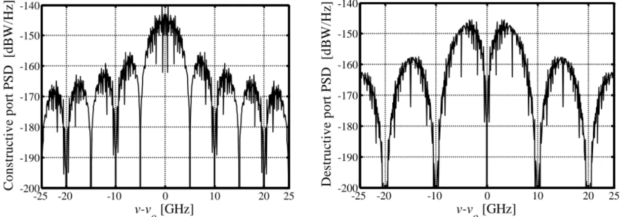
e define the coupling coefficient and the optical phase error, respectively. The influence of the optical phase error in the performance of the optical DPSK receiver is analyzed in subsection 3.5. Ideally, there is no optical phase error leading to a perfect constructive or destructive interference at the interferometer output ports [6].Figure 2.5 depicts the PSDs at each interferometer output, the signal E t at the 2( ) constructive port (left) and the signal E t at the destructive port (right). 1( )
Figure 2.5 – PSDs of signals 2(t) at constructive port (left) and 1(t) at destructive port (right).
The PSDs of both branches are in agreement with the PSDs shown in [6] and indicate that the simulation of the DPSK signaling and detection is implemented correctly.
The dual photodetector uses two positive intrinsic negative (PIN) photodiodes. The function of a photodiode is to convert the optical power into an electrical current in order to recover the transmitted data. A dual photodetector generates two photocurrents, i t and 1( )
2( ),
i t proportional to the optical powers p t1( ) and p t2( ) incidents in each photodiode of the dual receiver. These photocurrents i t1( ) and i t2( ) are given by
1 1 + 2 2 ( ) ( ) , ( ) ( ) i t R p t i t R p t (2.12)
where and , correspond to the responsivity of each photodiode in constructive and destructive branch, respectively, and are expressed in Ampere/Watts (A/W). The responsivity of a photodiode is defined by -25 -20 -10 0 10 20 25 -200 -190 -180 -170 -160 -150 -140 v-v o [GHz] Co n st ru ct iv e p o rt PSD [d BW /H z] -25 -20 -10 0 10 20 25 -200 -190 -180 -170 -160 -150 -140 v-v o [GHz] D es tru ct iv e p o rt PSD [d BW /H z]
2. Theoretical concepts 12 , o q R hv (2.13)
where and
q
are the photodiode quantum efficiency and the electron charge, respectively. The currents i t and 1( ) i t2( ) depend on two signals: the signal at MZDI input, E ta( ) and the MZDI input signal with a bit period delay, E t Ta( ). At the photodetector output if( )
a
E t and E t Ta( ) are equal, in the constructive port, the expected signal is a bit ‘1’. Otherwise, in the constructive port, the expected signal is a bit ‘0’. In the destructive port, the inverse process of the constructive port is observed for the signal.
Accordingly with (2.11), the optical powers at the dual photodetector output in the upper and lower branch, and neglecting the ASE noise, are defined, respectively, by
* 1 1 1 2 2 2 2 * ( ) ( ). ( ) 1 2 (1 ) ( ) ( ) je a a a a p t E t E t E t E t T E t E t T e (2.14)
* 2 2 2 2 2 * ( ) ( ). ( ) (1 ) 2 ( ) ( ) je a a a a p t E t E t E t T E t E t E t T e (2.15) with
2
2 a s os E t GP E t (2.16) and
* ( ) ( ) je cos ( ) , a a s os os e E t E t T e GP E t E t T t (2.17)where, [.] defines the real part of a complex number and ( )t is given by
( )t t t T .
(2.18)
The difference between these two photocurrents produces the photocurrent i t( ),
2 1
( ) ( ) ( ).
i t i t i t (2.19)
13
2 2 2 (1 2 ) ( ) ( 2 3 1) ( ) ( ) . 4 (1 ) cos ( ) a a s os os e E t T E t i t R GP E t E t T t (2.20)Considering 0.5, and Eos
t as an unitary amplitude, i t( ) is given by,
( ) scos ( ) e .
i t R GP t (2.21)
The signals at the dual photodetector output, i t and 1( ) i t2( ), and the photocurrent i t( )
are represented in Fig. 2.6, with e 0.
Figure 2.6 – Photocurrents, i1(t), i2(t) and i(t).
The signal detection can be done at the constructive port output, accordingly with Fig. 2.6, but for this situation the receiver sensitivity advantage of approximately 3 dB of a balanced DPSK receiver over an OOK reception is lost [6].
2.3.3. Electrical filter and decision circuit
After passing through the MZDI and the dual photodetector, the signal passes by an electrical filter, which can model the frequency limitations of the photodetectors. The electrical filter is described by the impulsive response h t and by the electrical bandwidth e( )
e
B at –3 dB. At the electrical filter output, the current of the signal is given by ( ) ( ) ( ).
b e
2. Theoretical concepts
14
At the decision circuit, the current i tb( ) is sampled every bit period and each sample is compared with a threshold level in order to decide which bit has been transmitted [16]. In a DPSK receiver, the threshold level is typically zero.
The electrical circuitry at the optical receivers generates circuit noise [3, chap. 5]. However, due to the high gain of the optical amplifier, the ASE noise beatings dominate over the circuit noise and, hence, in this work, circuit noise is neglected in the DPSK receiver performance evaluation [17].
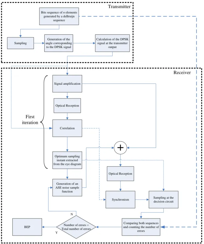
Figure 2.7 shows the simulated bits at the decision circuit output.
Figure 2.7 – Signal at the decision circuit output.
The signal representation at the DPSK output receiver in Fig. 2.7 is the same as the NRZ signal representation at the DPSK output transmitter in Fig. 2.3.
2.4. Implementation of the Monte Carlo simulator 2.4.1. Signals simulation
The main goal of this work is to create a simulation tool capable of evaluating the performance of the optical DPSK communication system, by calculating its bit error probability (BEP) and the impact of the in-band crosstalk in the system performance. The simulation involves the generation of the signals, its processing and the modeling of several devices.
The simulated signals in Matlab® are represented by discrete vectors, in time and frequency. Each vector position is indexed to a time instant, corresponding to a continuous signal sample. The length of time and frequency vectors is the same, and it is equal to the multiplication of the number of samples per bit (Na) and the number of bits (Nb) considered in the simulation. 0 1 2 3 4 5 6 7 8 9 10 11 12 13 14 15 16 -1 -0.5 0 0.5 1 A m pl it ud e t/Tb
15 In the simulation, a pseudorandom binary sequence with all possible combinations of
b bits and length Nb 2b bits is generated using deBruijn sequences [18, chap. 7]. This ensures that all bit patterns of length b are taken into account when studying ISI in a
communication system with memory length (measured in bit intervals) of b If the system . memory is higher than b, a higher number of bits must be simulated in order to more rigorously consider the effect of ISI on the system performance. Then, in order to consider ISI inside a bit period of Tb, the bits sequence is sampled Na times, generating a sampling sequence with (N Nb a) positions, with a corresponding time length of (N Tb b). The sampling time is Ta Tb/Na. 0 a N Time samples a T b a a T N T 2Tb
N Nb a1
TaFigure 2.8 – Simulated time vector.
Figure 2.8 shows the simulated time vector. Each n position of the time vector
corresponds to the time instant (n1)Ta at which a sample of the continuous signal is taken.
0 f 2 a f f 2 a f f
Figure 2.9 – Simulated frequency vector.
Figure 2.9 shows the simulated frequency vector. The signal representation in frequency is obtained using the fast Fourier transform (FFT), an algorithm which calculates the Discrete Fourier Transform (DFT)1 of the sampled discrete signal [18, chap. 3]. If the vectors lengths are not 2 ,b the algorithm used is much slower2 [18, chap. 3].
1
The result from the FFT must be multiplied by Ta because the FFT algorithm is not equivalent to the DFT. By
the same reason, the result of an inverse fast Fourier (IFFT) must be divided by Ta. If a pair FFT/IFFT is applied,
this correction factor is not necessary, since its transform effect is cancelled out.
2 The FFT requires that the vectors length must be 2N where N is an integer number, due to the algorithm
2. Theoretical concepts
16
The vector which represents the signal is shifted in frequency. The fftshift Matlab function must be applied to visualize the signal spectrum in its appropriate order. The frequency vector, first shows the positives frequencies 0,
2 a f f
and then the negatives
, 2 a f f
, where fa 1/Ta is the sampling frequency and f is given by
1 , b b f N T (2.23)
which defines the resolution of the frequency vector. From (2.23), to increase the resolution in the frequency, a higher number of bits should be simulated. A higher number of samples per bit, Na increases the sampling frequency and consequently, the frequency window.
2.4.2. Monte Carlo simulation
A MC simulation is a tool that allows the study of a random phenomenon by generating sequences of random numbers that represent the sample functions of the random phenomenon. Model of a Communication System Input ( ) ( ) X t N t Y t( ) Output
Figure 2.10 – Block diagram of the Monte Carlo simulation.
Figure 2.10 shows the block diagram of a MC simulation, where X t( ) is a deterministic signal, N t( ) is the random process at the communication system input and
( )
Y t is the signal obtained at the communication system output. A MC simulation generates random sample functions of N t( ),which are added to X t( ) and passed through the communication system. The statistical properties (e.g. probability density function) of the signal Y t( ) are measured at the communication system output [18, chap. 7].
Initially, the random process considered in the simulation is the ASE noise introduced by the EDFAs. The ASE noise field3 [19], in one polarization, is modeled as an additive white
3 A common normalization used in the literature consists in the multiplication of the ASE noise field by the
17 Gaussian noise (AWGN) process with in-phase N ti( ) and quadrature N tq( ) components related by 1 ( ) ( ) ( ) ( ) . 2 ASE i q s E t N t N t jN t e (2.24)
Each noise component sample function is generated using a generator of a Gaussian distributed numbers4, considering a zero mean and a variance equal to SASEfa,where fa is equivalent to the simulation bandwidth, Bs. The MC simulation is performed by generating a number of ASE noise sample functions sufficiently high enough to provide an accurate description of the statistical properties of Y t( ).
The PSD can be estimated using the periodogram definition [20]. After observing a sample function Y(t) over a long time interval T, the PSD can be estimated by
2 1 ( ) ( ) , y i G f Y f T (2.25)
where Yi ( f ) represents one sample function of Y (t) in the frequency domain. The signal
average power over a time interval Ts is given by [21]
2 1 ( ) . s s T p Y t dt T
(2.26)In the MC simulation, the signal average power is determined by the trapezoidal5 numerical integration.
2.4.3. The Monte Carlo simulation flowchart
The flowchart presented in Fig. 2.11 shows the implemented MC simulator of the optical DPSK receiver impaired by the ASE noise.
Firstly, at the transmitter a pseudorandom binary sequence is generated using deBruijn sequence. This generated sequence is sampled and, then, the angles ( )t corresponding to the phase of the DPSK signal are calculated using (2.5). Subsequently, the DPSK signal at the transmitter output is obtained using (2.2).
4 In Matlab®, this function is implemented using randn.m. 5
2. Theoretical concepts
18
Bits sequence of n elements generated by a deBruijn sequence Generation of the angle corresponding to the DPSK signal Calculation of the DPSK signal at the transmitter
output
Signal amplification
Generation of an ASE noise sample
function
Synchronism
Comparing both sequences and counting the number of
errors Number of errors =
Total number of errors BEP N Y Transmitter Sampling Sampling at the decision circuit Optical Reception Correlation Optical Reception Receiver First iteration
+
Optimum sampling instant extracted from the eye diagramFigure 2.11 – Flowchart of the MC simulation for a back-to-back configuration.
At the receiver input, and considering a back-to-back configuration, the optical signal is amplified. In the first iteration, the MC simulation is performed without noise, and the amplified signal passes through the optical receiver. The received signal is then correlated with the signal at the optical amplifier input, in order to identify the time propagation delay of the optical receiver, and after that the optimum sampling time is extracted from the eye
19 diagram. Then, a new random ASE noise sample function is generated and added to the amplified signal. The ASE noise sample added to the amplified signal passes through the optical receiver and is synchronized using the estimated propagation delay and the optimum sampling time. After synchronization and sampling, each received bit is compared with the bit of the deBruijn sequence to determine the number of errors, N In the next iterations, the e. number of errors from the previous iterations is added to the number of errors obtained in the current iteration. The cyclical process ends when the number of erroneous bits is the same as the total number errors, Ne, initially imposed for a specific accuracy of the MC simulation. The simulation process ends with the calculation of the BEP.
Correlation and Synchronization
The correlation process which is imposed at the first iteration on the receiver is necessary to determine the time propagation delay along the optical reception and allows to construct the eye diagram at the decision circuit input. This delay is used to synchronize the received sequence with the original sequence, in order to decide if the received bit has an error. The optimum sampling instant is extracted from the eye diagram considering the maximum eye opening and it is used in the decision to sample the received DPSK signal.
Calculation of the Bit Error Probability
In the MC simulation, the BEP is estimated through direct-error counting by
, ( 1) e it b N BEP N N (2.27)
where Nit is the number of iterations of the MC simulator.
In the MC simulation, the first bit of the received DPSK signal is excluded, since it depends on a previous bit, which is outside the time window of the simulator.
21
3. Optical DPSK communication system impaired by ASE noise
3.1. Introduction
In this chapter, the performance of an optical DPSK communication system impaired by ASE noise is investigated in a back-to-back configuration using MC simulation. Section 3.2 presents the model and characterization of the filters considered in the simulations. In section 3.3, the implementation of the MC simulation is validated by comparison of its BEP estimates, with the estimates of the analytical formulation proposed in [7], developed to assess the performance of optical DPSK communication systems. Notice that the analytical formulation [7] is derived for an isolated DPSK symbol, while the MC simulation is run with a sequence of Nb bits. Section 3.4 shows the performance of the optical DPSK balanced receiver studied for different optical and electrical filter combinations. In section 3.5, two DPSK receiver imperfections are studied: the interferometer detuning and the responsivity imbalance. The MC simulation is validated once again by comparison of its BEP estimates, with the estimates of the analytical formulation developed in [7] and with the results obtained in [22]. Table 3.1 shows the parameters considered to evaluate the performance of the optical DPSK communication system. Unless stated otherwise, these parameters are used throughout this chapter.
Table 3.1. Parameters of the simulated optical DPSK communication system impaired by ASE noise.
Parameter Value
Number of bits (Nb) 64 Number of samples (Na) 256 Number of erroneous bits (Ne) 100 EDFA gain (G) 30 dB Responsivity(R,R) 1A/W
Amplified noise figure (Fn ) 5 dB Bit period (Tb) 0.1 ns
Polarizer Present
3. Optical DPSK communication system impaired by ASE noise
22
3.2. Filters characterization
In this section, the filters used in the simulation are described and its main characteristics are analyzed. B is defined as the –3 dB bandwidth of the optical filter and o Be
is the –3 dB bandwidth of the electrical filter.
3.2.1. Ideal filter
The impulse response of an ideal optical filter (lowpass equivalent definition) is given by [23],
( ) sinc ,
o o o
h t B B t (3.1)
and its transfer function is given by,
=rect . o o f H f B (3.2)An ideal optical filter passes exactly all the signal frequencies inside its passband bandwidth and completely rejects the others. Figure 3.1 represents the ideal optical filter transfer function for B To b100.
Figure 3.1 – Ideal filter transfer function for BoTb = 100.
3.2.2. Gaussian filter
The Gaussian filter is used as an optical filter and as an electric filter, where Be2Bo. The impulse response of an optical Gaussian filter is given by [24],
23 2 2 2 .( ) ln 2 2 2 ( ) . , ln 2 2 o B t o B h t e (3.3)
with transfer function given by,
22 2 =exp . ln 2 o f H f B (3.4)Notice that the Gaussian filter has a zero phase response and is usually used in the optical communication systems, because its frequency response is similar with the transfer function of an arrayed-waveguide grating [24].
3.2.3. Lorentzian filter
The impulse response of a Lorentzian optical filter is given by [25], ( ) B to, 0
o
h t B e t (3.5)
where its transfer function is given by,
1 . 1 2 o H f f j B (3.6)Fabry-Perot filters are widely used in optical transmission systems and their response can be approximated by a Lorentzian impulse response [26].
3.2.4. Integrator filter
The integrator filter is only used as an electrical filter. The impulse response of an integrator filter is given by [7],
( ) b t h t rect T (3.7)
where its transfer function is given by,
bsinc
b .H f T fT (3.8)
3. Optical DPSK communication system impaired by ASE noise
24
Figure 3.2 – Electrical integrator filter transfer function for BeTb = 1.
3.2.5. RC filter
The RC filter is an electrical filter with impulse response given by [7],
2
( ) 2 B te , 0
e
h t B e t (3.9)
with transfer function defined by,
1 . 1 e H f f j B (3.10)Figure 3.3 depicts the amplitude response of the Gaussian and Lorentzian optical filters with a –3 dB bandwidth Bo 100GHz.
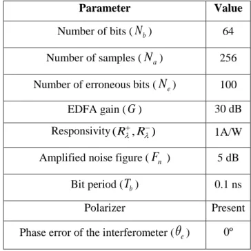
Figure 3.3 – Amplitude response of the Gaussian and Lorentzian optical filters.
-100 -80 -60 -50 -40 -20 0 20 40 50 60 80 100 -12 -10 -8 -6 -4 -3 -2 0 v-v o [GHz] A m pl it ude [ dB ] Gaussian filter Lorentzian filter
25 Accordingly with Fig. 3.3, it can be visualized that the Gaussian optical filter is more selective than the Lorentzian optical filter because its amplitude response is flatter inside its passband and exhibits a highest rejection.
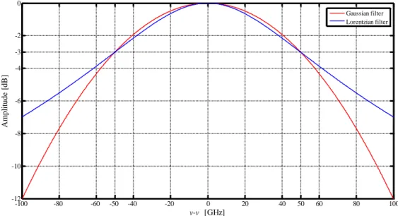
Figure 3.4 presents the amplitude response of the Gaussian and RC electrical filters, for a –3 dB bandwidth of Be 7GHz.
Figure 3.4 – Amplitude response of the Gaussian and RC electrical filters.
From Fig. 3.4, it can be concluded that the Gaussian electrical filter is again more selective than the RC electrical filter because the Gaussian filter has a flatter amplitude response in the cut-off frequency. The RC filter presents a lowest rejection in the amplitude response, which can lead to more degradation in the simulation, due to higher filtered ASE noise power.
The Lorentzian and RC filters are the only filters considered in this work that have a phase response, and consequently a delay response. Although, the Lorentzian filter being an optical filter and the RC filter an electrical filter, they exhibit the same response since their definition is identical [see (3.6) and (3.10)].
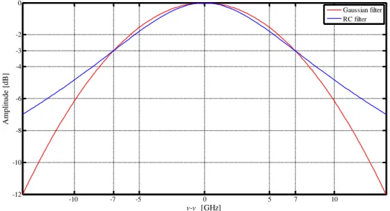
Figure 3.5 shows the group delay response of a RC electrical filter, for the –3 dB bandwidths Be 3.5, 7, 10 and 13 GHz. -10 -7 -5 0 5 7 10 -12 -10 -8 -6 -4 -3 -2 0 v-v o [GHz] A m pl it ude [ dB ] Gaussian filter RC filter
3. Optical DPSK communication system impaired by ASE noise
26
Figure 3.5 – Group delay of the RC filter for different electrical filter –3 bandwidths.
From Fig. 3.5, it can be concluded that RC electrical filter with smaller bandwidths exhibit a higher group delay. As the bit rate considered in this work is 10 Gbps, electrical filters with a –3 dB bandwidth of 3.5 GHz would lead to a severe signal degradation due to their higher delay distortion. Even for Be 7GHz, the delay distortion (inside the bandwidth of 10 GHz) is about 15 ps, i.e., about 15% of the bit period, and so a higher performance degradation is expected.
3.3. Validation of the Monte Carlo simulation
In this section, the MC simulation is validated by comparison with the analytical formalism developed in [7] for an isolated DPSK symbol. This analytical formalism can consider arbitrary optical and electrical filtering at the optical DPSK receiver. Notice that this validation is accomplished by comparison of BEP estimates obtained using the MC simulation with the estimates calculated by the analytical formalism [7]. The accuracy of the MC simulation BEP estimates with the number of bits and the number of errors used in the simulation is also studied. In this subsection, all the MC simulations are obtained for an ideal optical filter (OF) and an integrator electrical filter (EF). The bandwidth of the electrical filter is always the same, Be = 10 GHz.
In this section, the BEP estimates obtained from the MC simulation are depicted with a solid line or with a legend (S), while the BEPs obtained with the analytical formalism are depicted with a dashed line or with a legend (A).
-500 -40 -30 -20 -10 0 10 20 30 40 50 10 20 30 40 50 v-v o [GHz] G roup de la y [ps ] BoTb= 3.5 GHz B oTb= 7 GHz B oTb= 10 GHz B oTb= 13 GHz 15 ps
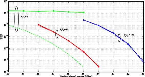
27 Figure 3.6 shows BEP estimates of the MC simulation, as a function of the optical signal power for different optical filter –3 dB bandwidths, compared with the BEP estimates of the analytical formalism [7]. The optical signal power is obtained at the optical pre-amplifier input.
Figure 3.6 – BEP as a function of the optical signal power, for the ideal OF and the integrator EF combination, considering BoTb = 1, 10 and 100.
As the MC simulation is obtained with a sequence of bits, it takes into account the ISI effect on the DPSK receiver performance. As the analytical formulation neglects this effect, for smaller normalized optical filter bandwidths
B To b 1 ,
the BEPs estimated from the MC simulation and the analytical formulation are very discrepant. For normalized higher optical filter bandwidths
B To b 10, 100 ,
the simulated results are very similar to the results obtained with the analytical formulation, and the MC simulator can be considered validated for this situation.Figure 3.6 also shows that, for the same optical signal power, there is a severe increase of the BEP with the optical filter bandwidth enlargement. This occurs because with the increase of the optical filter bandwidth, the filtered ASE noise power is higher, and the receiver performance is degraded.
Figure 3.7 depicts the BEPs obtained with the MC simulation and with the analytical formalism [7], for normalized optical filter bandwidths, where the ISI effect on the performance is relevant [BoTb 2].
3. Optical DPSK communication system impaired by ASE noise
28
Figure 3.7 – BEP as a function of the optical signal power, for the ideal OF and the integrator EF combination considering smaller normalized optical filter bandwidths.
Accordingly with Fig. 3.7, it can be assumed that the simulated results become similar to the analytical results above B To b 2. This means that the ISI effect starts to lose its influence as the dominant source of performance degradation and provides a reference for the optical filter bandwidth above which, the precision of the analytical formalism (that neglects ISI) is ensured. It is important to notice that the ISI effect on the performance depends on the optical and electrical filters combination.
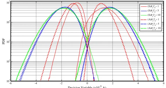
Figure 3.8 depicts the probability density function (PDF) for B To b equal to 1 (red), 5 (blue) and 10 (green), using an optical signal power of –47dBm.
Figure 3.8 – PDF of the decision variable, for the ideal OF and the integrator EF combination, considering
an optical signal power with –47 dBm and BoTb = 1, 5 and 10.
-6 -4 -2 0 2 4 6 x 10⁻⁵ 101 102 103 104 105 Decision Variable (x10-5 A) P D F 1 1.5 2 2.5 3 3.5 4 4.5 5 5.5 6 -2 0 2 4 6 8 10 12 14 16 (S)BoTb= 1 (S)BoTb= 5 (S)B oTb= 10 (A)B oTb= 1 (A)BoTb= 5 (A)B oTb= 10
29 The estimates of the MC simulation and the analytical formalism from [7] are represented by the solid and dashed curves, respectively. Accordingly with Fig. 3.8, a very good agreement is found between the PDFs estimated using both methods, for BoTb = 5 and
BoTb = 10, which ensures again the validation of the MC simulation implementation. Only for
smaller normalized optical filter bandwidths, near BoTb = 1 there exists a difference between
the PDFs of the bits ‘0’ and ‘1’, calculated using MC simulation and the PDFs estimated analytically. The ISI effect on the PDFs assumes the highest relevance with the decrease of the bandwidth of the optical filter, especially for smaller normalized optical filter bandwidths,
1,
o b
B T which leads to a growing asymmetry between the PDFs of the bits ‘0’ and ‘1’ and to an optimum decision threshold deviation from zero to negative values. This asymmetric behavior does not occur on the analytical formalism [7], because this formalism assumes an isolate DPSK symbol and neglects the ISI effect. The PDFs asymmetric behavior (observed in the MC simulation) is in agreement with the results presented in [27], which also consider a sequence of bits to obtain the PDFs.
Figure 3.8 also shows that for B To b 1, the optimum decision threshold is near zero and the PDFs crossing points increases with the increase of BoTb, which means that higher
BEPs are achieved due to the higher ASE noise power.
Figure 3.9 shows the eye diagrams at the decision circuit input for the ideal OF and the integrator EF, consudering B To b equal to 1 (left), 5 (middle) and 10 (right), using an optical signal power of –47dBm.
Figure 3.9 – Eye diagram at the decision circuit input for the ideal OF and the integrator EF combination, considering BoTb equal to 1 (left), 5 (middle) and 10 (right).
0 1 -2 -1 0 1 2 3x 10 -5 Normalized time Cu rren t (x 1 0 -5 A ) 0 1 -2 -1 0 1 2 3x 10 -5 Normalized time Cu rren t (x 1 0 -5 A ) 0 1 -2 -1 0 1 2 3x 10 -5 Normalized time Cu rren t (x 1 0 -5 A )