PARAMETRIC ANALOG SIGNAL
AMPLIFICATION APPLIED TO NANOSCALE
CMOS WIRELESS DIGITAL TRANSCEIVERS
PARAMETRIC ANALOG SIGNAL
AMPLIFICATION APPLIED TO NANOSCALE
CMOS WIRELESS DIGITAL TRANSCEIVERS
Thesis presented in partial fulfillment of the requirements for the degree of Doctor
of Philosophy in the subject of Electrical and Computer Engineering by the Universidade Nova de Lisboa, Faculdade de Ciências e Tecnologia.
The atoms left their heavenly path,
And by fortuitous embraces,
Engendered all that being hath.
And though they seem to cling together,
And form ’associations’ here,
Yet, soon or late, they burst their tether,
And through the depths of space career.
James Clerk Maxwell (1874)
This page would be always small to cope for the acknowledgments that I would like to publicly express to many people that have followed me along this journey.
First and foremost, I strongly acknowledge my supervisors Prof. A. Steiger Garção and Prof. João C. Goes.
I am sincerely grateful to Prof. A. Steiger Garção whose expertise, guidance, support, and patient have made this work possible. His personal and original view on electronics have broken me barriers and opened doors into this amazing scientific and technological world.
I would like to express my personal and deep gratitude to Prof. João C. Goes for his support, availability, encouragement and motivation, deep technical competence, commitment, orientation. He his the mentor for many of the breakthrough that made possible the work to pursuit towards the final objective.
I also would like to deeply acknowledge Prof. Yannis Tsividis for his kind encourage-ment and useful remarks. The suggestions kindly sent by Prof. Yannis Tsividis, about the MOS Parametric Cell, have been absolutely crucial to understand the operation details of this circuit.
To my colleagues and friends, Nuno Paulino for the deep technical discussions, Rui Tavares for his CAD support and to Luís Oliveira for the fruitful discussions on radio transceivers.
To Prof. Jorge Fernandes from INESC-ID who was always a unconditional supporter for this work with very helpful contributions.
Definitively to João Ferreira, Michael Figueiredo, Edinei Santin, José Custódio, Bruno Esperança for all the support and work performed. To Erik Snelling, João Faria, from Silicon and Software Systems(S3) for the lab support.
To José Faustino from INESC-ID for the excellent chip on board work.
• Department of Electrical Engineering of the FCT-UNL that provided the neces-sary conditions to realize the work,
• CTS-UNINOVA that provided the necessary conditions to realize the work,
• Fundação para a Ciência e Tecnologia that supported part of this work through the projects SPEED, LEADER and IMPACT.
I thank my parents and sister family, for their existence and unconditional friendship.
To my wonderful wife Lúcia and my son João, for their unconditional and persistent help, encouragement, motivation and support.
A atenuação que inevitavelmente ocorre na propagação de um sinal rádio entre a antena emissora e o receptor motivou uma procura persistente no domínio da amplificação electrónica de sinal. Todavia, o indissociável ruído existente quer no canal quer no dispositivo de amplificação em si torna a tarefa de recuperação do sinal original bem mais complexa.
Uma das formas de amplificação electrónica, surgida em meados do século passado, assenta na utilização de uma capacidade variável não linear. Através desta última é possível misturar o sinal de entrada com um outro fornecido por uma fonte auxiliar e forçar a transferência de energia entre as diversas componentes espectrais entretanto originadas. Desta forma e sob determinadas condições, é possível construir-se um amplificador paramétrico cujo o processo de amplificação é intrinsecamente ausente de ruído uma vez que não é baseado numa transconductância mas sim na variação paramétrica de uma reactância.
Apesar da técnica acima referida ser conhecida há várias décadas, apenas recentemente foram apresentados alguns exemplos da sua utilização na tecnologia CMOS. Nestes exemplos incluem-se aplicações quer no domínio do tempo contínuo quer em tempo discreto. A amplificação paramétrica em tempo discreto assenta na alteração periódica da capacidade do dispositivo MOS, obtida através da alteração forçada do seu regime de funcionamento enquanto mantém aprisionadas as cargas entretanto armazenadas na porta do dispositivo. Esta alteração da capacidade, enquanto se mantém a carga constante, terá de ser compensada por uma variação correspondente da tensão aos ter-minais do dispositivo. A amplificação do sinal assim obtida não depende directamente da transcondutância associada ao transístor MOS o que a torna uma opção a ter em conta no projecto de circuitos analógicos em tecnologias submicrométricas. Pretende-se, com o recurso a esta técnica, potenciar a utilização de células de amplificação com ganho reduzido e em malha aberta como forma de contornar as crescentes dificuldades de integração de amplificadores operacionais devido ao escalonamento verificado na tecnologia CMOS.
transreceptores rádio. É neste contexto que são analisados diversos circuitos que podem integrar amplificação paramétrica, nomeadamente, um comparador, um misturador passivo e, inclusivamente, um conversor analógico-digital. Dada a funcionalidade absolutamente fundamental de um conversor analógico-digital num receptor rádio dig-ital, demonstra-se experimentalmente a viabilidade da utilização da técnica através da integração, numa tecnologia CMOS de 130 nm, de um conversor analógico-digital de velocidade moderada com 8-bits de resolução e 120 MS/s de frequência de amostragem efectiva. Prova-se dessa forma e após caracterização experimental, que é possível construir um conversor analógico-digital que apenas utiliza dispositivos MOS e sem recurso a amplificadores operacionais de alto desempenho e consumo. Destes factos resulta a consolidação de uma técnica alternativa de processamento analógico de sinal que vem contribuir para o desenvolvimento de circuitos no seio das mais recentes tecnologias CMOS nanométricas.
Signal amplification is required in almost every analog electronic system. However noise is also present, thus imposing limits to the overall circuit performance, e.g., on the sensitivity of the radio transceiver. This drawback has triggered a major research on the field, which has been producing several solutions to achieve amplification with minimum added noise. During the Fifties, an interesting out of mainstream path was followed which was based on variable reactance instead of resistance based amplifiers. The principle of these parametric circuits permits to achieve low noise amplifiers since the controlled variations of pure reactance elements is intrinsically noiseless. The amplification is based on a mixing effect which enables energy transfer from an AC pump source to other related signal frequencies.
While the first implementations of these type of amplifiers were already available at that time, the discrete-time version only became visible more recently. This discrete-time version is a promising technique since it is well adapted to the mainstream nanoscale CMOS technology. The technique itself is based on the principle of changing the surface potential of the MOS device while maintaining the transistor gate in a floating state. In order words, the voltage amplification is achieved by changing the capacitance value while maintaining the total charge unchanged during an amplification phase.
Since a parametric amplifier is not intrinsically dependent on the transconductance of the MOS transistor, it does not directly suffer from the intrinsic transconductance MOS gain issues verified in nanoscale MOS technologies. As a consequence, open-loop and opamp free structures can further emerge with this additional contribution.
This thesis is dedicated to the analysis of parametric amplification with special empha-sis on the MOS discrete-time implementation. The use of the latter is supported on the presentation of several circuits where the MOS Parametric Amplifier cell is well suited: small gain amplifier, comparator, discrete-time mixer and filter, and ADC. Relatively to the latter, a high speed time-interleaved pipeline ADC prototype is implemented in a standard 130 nm CMOS digital technology from United Microelectronics Corporation
speed opamp has not been used in the signal path, being all the amplification steps implemented with open-loop parametric MOS amplifiers. To the author’s knowledge, this is first reported pipeline ADC that extensively used the parametric amplification concept.
The dynamic performance of this ADC was experimentally evaluated and confirmed with 3 chip samples that were mounted the printed circuit board using a direct-bonding technique. Experimental results show that the measured DNL and INL errors at 120 MS/s are within 0.8/+1.4 LSB and±2.0 LSB, respectively. The measured FFT for a 20 MHz input signal frequency (fin) and 120 MS/s sampling frequency (Fs), demonstrates
that the circuit achieves a peak SNR of 39.7 dB, a SFDR of 49.3 dB and a peak THD of 47.5 dB, corresponding to an ENOB of 6.2 bits. The ADC features an active area below 0.12 mm2 and dissipates less than 14.5 mW at 120 MS/s and 1.2 V supply, resulting in standard figure of merit (FOM) better than 191 [fJ.mm2 per conversion].
γ Body effect coefficient
µ Carrier mobility
µ0 Magnetic Permeability
µn Carrier mobility
φ Clock phase
φF Fermi potential
φt Thermal voltage, 0.0259 V at 300 K
ψs Surface potential
AIGS Gate leakage mismatch factor
AV T H Threshold voltage matching parameter
cov Overlap capacitance
Cox Total Oxide capacitance
C′
ox Oxide capacitance per unit of area
clk Master clock
dBF S dB Full Scale
F Noise factor
fin Input signal frequency
Fs Sampling frequency
fT Transition frequency
gm Transconductance
k Boltzmann’s constant
L Channel length
lov Overlapped length
NA Acceptor concentration
ND Donor concentration
p Intrinsic parametric gain factor
q Unity charge
S Elastance
T Absolute Temperature
tox Oxide thickness
Vt0 Threshold voltage with zero bias
Vth Threshold voltage
VF B Flat band voltage
vsat Velocity saturation
W Channel width
3G 3rd Generation for Mobile Communications
A/D Analog-to-digital
ADC Analog-to-digital Converter
ATG Asymmetric Transmission Gate
BB Baseband
BiCMOS Bipolar and CMOS technology
BS Bulk-switching
BSIM4 Berkeley Short-channel IGFET Model version 4
BTBT Band-to-band-tunneling
BW Signal Bandwidth
CMOS Complementary Metal-Oxide-Semiconductor
CT Continuous Time
D/A Digital-to-analog
DAC Digital-to-analog Converter
DCR Direct Conversion Receiver
DIBL Drain-induced-barrier-lowering
DNL Differential Nonlinearity
DT Discrete Time
EDT Edge-direct-tunneling
ENOB Effective Number of Bits
FFT Fast Fourier Transform
FOM Figure-of-merit
FQ Flash Quantizer
GaAs Gallium Arsenide
GIDL Gate-induced-drain-leakage
GPRS General Packet Radio Service
GSM Global System for Mobile Communications
IF Intermediate Frequency
IGFET Insulated-Gate Field-Effect Transistor
INL Integral Nonlinearity
IP Internet Protocol
LTE 3GPP Long Term Evolution
MASER Microwave Amplification by Stimulated Emission of Radiation
MDAC Multiplying Digital-to-analog Converter
MIM Metal-insulator-metal
MOM Metal-oxide-metal
MOS Metal-Oxide-Semiconductor
MOSCAP MOS Capacitor
MOSFET MOS Field Effect Transistor
MPA MOS Parametric Amplifier
MSB Most Significant Bit
MTBA Multiply-by-two Amplifier
NF Noise Figure
NF Noise figure in dB
NMOS N-channel MOSFET
NQS Non-quasi-static
opamp Operational Amplifier
PAMP Parametric Amplifier
PAN Personal Area Network
PCB Printed Circuit Board
PFBL Positive Feedback Latch
PMOS P-channel MOSFET
PSTN Public Switched Telephone Network
PVT Process-supply-temperature
RF Radio Frequency
S/H Sample-and-hold
S/N Signal-to-noise Ratio
SC Switched Capacitor
SCE Short Channel Effects
SDR Software Defined Ratio
SF Source Follower
SFDR Spurious Free Dynamic Range
SICAS Semiconductor International Capacity Statistics
SINAD Signal-to-noise and Distortion Ratio
SNDR Signal-noise-plus-distortion Ratio
SNR Signal-to-noise Ratio
SoC System-on-chip
TG Transmission Gate
THD Total Harmonic Distortion
UWB Ultra WideBand
WiFi Standard for wireless local area networks
WLAN Wireless Local Area Network
WSpW Wafers per Week
Acknowledgments vii
Sumário ix
Abstract xi
List of Symbols and Acronyms xiii
List of Figures xxxi
List of Tables xxxiii
1 Introduction 1
1.1 Motivation and Scope . . . 1
1.2 Contributions of this work . . . 3
1.3 Thesis Organization . . . 4
2 Wireless system and circuit design space in modern digital CMOS technology 7 2.1 Introduction . . . 7
2.2 Wireless System Overview and Requirements . . . 8
2.3 CMOS Scaling Impose Challenges for Analog Design . . . 14
2.3.1 gm, gds, and transistor’s intrinsic gain . . . 16
2.3.4 Leakage and OFF state current . . . 21
2.3.5 Transistor’s Matching . . . 23
2.3.6 Passive components: MIM Capacitors and Inductors . . . 24
2.4 Architecture Considerations for RF Transceivers in Submicron CMOS . 25 2.4.1 SuperHeterodyne Receiver . . . 26
2.4.2 Zero-IF and Low-IF receivers . . . 27
2.4.3 Universal Software Defined Radio (USDR) . . . 29
2.4.4 Receiver with (sub)sampling . . . 30
2.4.5 Energy Detector based Receiver . . . 33
2.5 Emerging circuit design strategies for CMOS nanoscale wireless transceivers 34 2.5.1 Digital assisted analog approach . . . 34
2.5.2 Open Loop and reactance based amplifiers . . . 35
2.6 Summary . . . 37
3 Parametric Signal Amplification in Continuous Time Domain 39 3.1 Introduction . . . 39
3.2 Using a reactance to build a transistor-free amplifier . . . 40
3.3 Varactors in CMOS technology . . . 48
3.4 Manley-Rowe power relations for nonlinear reactances . . . 51
3.5 CMOS parametric amplification with frequency conversion in continuous time domain . . . 54
3.6 Summary . . . 59
4 Discrete Time Parametric Amplification in digital CMOS technology 61 4.1 Introduction . . . 61
4.3 Implementation of a Discrete-Time MOS Parametric amplifier . . . 67
4.4 Analysis of the discrete-time MPA cell as an amplifier . . . 70
4.4.1 Amplification Gain . . . 71
4.4.2 Harmonic distortion . . . 81
4.4.3 Time response (speed) . . . 87
4.4.4 Noise analysis . . . 93
4.4.5 MPA cell design . . . 96
4.5 Some applications of the MPA cell . . . 100
4.5.1 A Multiply by Two Amplifier (MTBA) . . . 100
4.5.2 Comparator . . . 106
4.5.3 A Mixer for a discrete-time receiver . . . 110
4.6 Summary . . . 115
5 Design of a pipeline ADC fully based in MOS parametric amplifica-tion 117 5.1 Introduction . . . 117
5.2 Description of the ADC architecture . . . 118
5.3 Analog Building blocks . . . 121
5.3.1 Full time-interleaved pipelined stage . . . 121
5.3.2 MDAC for the 1.5-bit pipelined stage . . . 124
5.3.3 Flash quantizers for the 1.5-bit and 2-bit stages . . . 125
5.3.4 Replica bias circuit (RBC) . . . 129
5.3.5 The front-end S/H circuit . . . 130
5.4 Digital logic and Clock Generation . . . 132
5.4.1 Digital synchronization logic . . . 132
5.4.2 Digital correction logic . . . 133
5.6 Overall ADC simulation . . . 136
5.7 Summary . . . 137
6 Integrated prototype and experimental evaluation 139
6.1 Introduction . . . 139
6.2 Integrated prototype . . . 140
6.2.1 Full chip . . . 140
6.2.2 Layout of the different building blocks . . . 142
6.2.3 Overall ADC post layout simulations . . . 147
6.3 Test bench . . . 148
6.3.1 Printed circuit board used in testing . . . 148
6.3.2 Test setup . . . 149
6.4 Measurement Results . . . 150
6.5 Summary . . . 156
7 Conclusions and Future Work 159
7.1 Conclusions . . . 159
7.2 Future Work . . . 161
A One approach for RF front-end receiver design 163
A.1 Introduction . . . 163
A.2 Low Noise Amplifier . . . 164
A.3 Frequency translation . . . 168
A.4 Co-design and merging strategies . . . 170
Appendices 163
Bibliography 184
Index 198
1.1 Comparative evolution of the Bipolar and MOS installed wafer produc-tion capacity, based on data available from SICAS. . . 2
2.1 Shannon channel capacity. . . 10
2.2 Simplified point to point communication model. . . 10
2.3 All IP network architecture approach. . . 12
2.4 Multimedia wireless equipment (OpenMoko) and wireless sensor node (BTNode). . . 13
2.5 Transit frequency comparison between CMOS and Bipolar technology. . 14
2.6 NFmin versus fT. . . 20
2.7 Ideal digital receiver. . . 26
2.8 Heterodyne receiver. . . 27
2.9 Low-IF or Zero-IF receiver. . . 28
2.10 Universal software defined radio. . . 30
2.11 IF subsampling receiver architecture. . . 31
2.12 Spectrum transformation in a subsampling receiver. . . 32
2.13 UWB receiver with direct subsampling. . . 33
2.14 Envelope detection receiver architecture. . . 34
2.15 Dynamic Source Follower Amplifier. . . 36
2.16 Voltage waveforms at the input and output of the Dynamic Source Follower Amplifier, without body effect (Vsb = 0). . . 37
3.1 Simple model for the parametric capacitor. . . 41
3.2 Equivalent model for a two-tank parametric amplifier. . . 43
3.3 Equivalent model for a two-tank parametric amplifier at resonance. . . 45
3.4 Model for a traveling wave parametric amplifier. . . 46
3.5 Simplified model of a MOSFET distributed amplifier. . . 47
3.6 P+ to n-well diode based varactor. . . 49
3.7 Accumulation mode MOS varactor. . . 50
3.8 Inversion mode MOS varactor. . . 51
3.9 Circuit model for the Manley-Rowe relations. . . 52
3.10 Equivalent simplified model for the parametric mixer. . . 55
3.11 Parametric downconvertion mixer gain and NF. . . 58
3.12 Simplified model of a MOSFET parametric down converter. . . 58
4.1 Conceptual discrete-time parametric amplifier. . . 62
4.2 Voltage gain versus normalized load capacitor (CL/Cφ1). . . 64
4.3 Gain improvement by applying parametric amplification to a S/H. . . . 65
4.4 Energy and voltage gain versus normalized load capacitance CL/Cφ1. . 66
4.5 Dynamic MOS logic with bootstrap varactor. . . 68
4.6 MOS parametric amplifier cell. . . 69
4.7 Total gate charge and capacitance for a pump source of 0 V and 1.2 V. 74
4.8 Model for the variation of the total gate charge, QG, for a pump source
of 0 V and VDD. . . 75
4.9 Comparison of the intrinsic parametric amplification gain obtained from (4.27) and (4.26). . . 77
nology. . . 77
4.11 Extrinsic capacitance model of the MPA cell. . . 78
4.12 The impact of the device length on the MPA cell gain. . . 79
4.13 MPA gain obtained for different combination of parasitic, overlap and load capacitances, in an 130 nm CMOS technology. . . 80
4.14 SPICE simulations obtained with NMOS MPA cell, in an 130 nm CMOS technology. . . 82
4.15 Harmonic distortion analysis, using parameters from a 130 nm standard CMOS technology. . . 84
4.16 Differential structure for the MPA cell based amplifier. . . 85
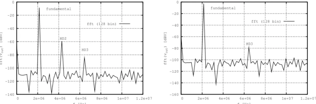
4.17 128 point based FFT obtained from SPICE simulations data, in a 130 nm CMOS technology. . . 86
4.18 MPA cell time response model. . . 88
4.19 MOS capacitance model. . . 88
4.20 Layout schematic for substrate resistance model. . . 90
4.21 MPA cell during track time period. . . 91
4.22 MPA cell during amplification and hold time period. . . 92
4.23 Simplified noise model for the MPA cell. . . 93
4.24 Modified MPA cell with two MOS devices: bottom-left - original “DS configuration”; bottom-right - modified “FT configuration”. . . 98
4.25 Discrete-time MPA with complementary structure. . . 100
4.26 Q-V analysis of the DT MPA with complementary structure. . . 101
4.27 CMOS discrete-time amplifier (MPA block) with output level shift control.102
4.28 Four MPA connected in a time interleaved structure. . . 103
4.29 Half MPA single-ended circuit (p version). . . 103
4.30 Replica bias block used to generate Vbias for the 2 source-followers used in the MBTA block. . . 105
ing at 100 MHz clock rate, and for a 10 MHz input signal. . . 106
4.33 Block diagram of the parametric based comparator. . . 107
4.34 Input SC network with embedded parametric amplification. . . 107
4.35 Comparator circuit schematic with embedded parametric amplification in the input SC network. . . 109
4.36 Monte Carlo simulations (800) to determine the input-referred offset of the comparator. . . 110
4.37 Electrical simulations to evaluate the worst-case time response of the comparator. . . 111
4.38 Discrete-Time and charge based FIR filter employing a MPA technique. 112
4.39 Discrete-Time Mixer with embeded MPA technique. . . 113
4.40 The effects of L variation on the DT-mixer gain and NF, for DCMPA
and FTMPA circuits. . . 114
4.41 Discrete-Time frequency response obtained from SPECTRE simulator, using an 130 nm CMOS technology. . . 115
5.1 Global architecture for the ADC. . . 120
5.2 Block diagram of a pipelined stage of the ADC (N-type). . . 122
5.3 The variation of the common-mode voltage along the pipeline. . . 123
5.4 MDAC conversion characteristic for a full-scale input ramp signal. . . . 124
5.5 N-Type Half-MDAc schematic. . . 124
5.6 Simplified schematic of the 1.5-bit FQ. . . 126
5.7 1.5-bit flash quantizer ideal transfer function. . . 126
5.8 2-bit flash quantizer. . . 127
5.9 Schematic of the comparator used in the FQs. . . 128
5.10 Schematic of the N-type RBC block. . . 129
5.12 Block diagram of the input S/H with gain of two. . . 131
5.13 Input S/H replica bias circuit. . . 131
5.14 Single-channel digital synchronization logic. . . 132
5.15 Digital error correction logic circuit for a single-channel ADC. . . 133
5.16 Clock phases timing diagram. . . 134
5.17 Schematic of the clock-phase generator used in the ADC. . . 135
5.18 MDAC simplified model for noise analysis. . . 135
5.19 Simulated 512 bins FFT spectrum . . . 137
6.1 Die photo of the test chip with overlaid layout plot. . . 140
6.2 Chip floorplan. . . 142
6.3 Layout of the time-interleaved pipeline stages (type N and P). . . 143
6.4 Layout plot of the 1.5-bit and 2-bit FQ. . . 144
6.5 Layout plot of one 50 mV comparator. . . 144
6.6 Layout plot of a time-interleaved MDAC of a N-type stage. . . 145
6.7 Layout plot of a RBC block used in a N-type stage. . . 146
6.8 Layout plot of the front-end S/H. . . 146
6.9 Example of a FFT obtained from post layout simulations. . . 148
6.10 PCB used for testing the chip, which was directly wire-bonded to the board. . . 149
6.11 Block diagram of the experimental test environment. . . 150
6.12 DNL experimental results from one sample. . . 151
6.13 INL experimental results from one sample. . . 151
6.14 Calculated FFT from experimental data obtained from one sample. . . 152
6.15 Measured ENOB versus fin (-0.1 dBFS and Fs = 120 MS/s). Results
obtained form 3 different chip samples. . . 152
6.17 Measured THD versus fin (-0.1 dBFS and Fs = 120 MS/s). Results
obtained form 3 different chip samples. . . 154
6.18 Measured THD versus Fs (-0.1 dBFS and fin = 20 MHz). Results
obtained form 3 different chip samples. . . 154
6.19 Measured SFDR versus fin (-0.1 dBFS and Fs = 120 MS/s). Results
obtained form 3 different chip samples. . . 155
6.20 Measured SFDR versus Fs (-0.1 dBFS and fin = 20 MHz). Results
obtained form 3 different chip samples. . . 155
6.21 Measured Power consumption versusFs(-0.1 dBFS and fin = 20 MHz).
Results obtained form 3 different chip samples. . . 156
A.1 Narrowband Low Noise Amplifiers. . . 165
A.2 Definition of the 1 dB compression point, IIP2 and IIP3. . . 166
A.3 Wideband LNAs. . . 167
A.4 Active and passive mixer. . . 169
A.5 RC Two-Integrator Oscillator circuit with quadrature outputs. . . 171
A.6 Linear model for the RC Two-Integrator Oscillator. . . 171
A.7 LNA, Mixer and LO circuit diagram. . . 172
A.8 SpectreRF PSS simulation results for the co-design of LNA, mixer and LO. . . 173
A.9 An LNA, mixer and Oscillator merged cell, LMV. . . 174
B.1 Basic Track and Hold circuit. . . 177
B.2 S/H errors. . . 178
B.3 Basic MOS switches. . . 179
B.4 Total conductance and resistance of the CMOS switch. . . 179
B.5 Charge injection and Clock feedthrough in NMOS switch. . . 180
B.7 Bottom plate sampling technique with an NMOS switch. . . 181
B.8 SLC technique applied in CMOS switch. . . 182
B.9 ADC evolution trends in last decade. . . 183
2.1 Summary of most common wireless network standards. . . 12
2.2 Theoretical CMOS scaling impacts. . . 15
2.3 IBM digital CMOS technology characterization. . . 18
3.1 Performance comparison between varactor in MOS technology. . . 51
4.1 Comparative harmonic distortion results. . . 87
4.2 SNR and THD for two sized single-ended MPA devices, combined or not, in a pseudo-differential structure. . . 96
4.3 Capacitances values during sampling and amplification phases. . . 99
4.4 Comparative results for the three sampling cell cases. . . 115
5.1 MOS device dimensions for the HMDAC. . . 125
6.1 List of all Pads used in the ADC prototype. . . 143
6.2 Difference between ENOB from both interleaved channels. . . 153
6.3 ADC key features and measured Results. . . 157
A.1 Simulation results for the co-design. . . 174
B.1 S/H circuit performance issues. . . 178
Introduction
1.1
Motivation and Scope
Silicon-based electronics has been one of the key factor contributing for the creation and refinement of modern and sophisticated end-user applications. Examples of these achievements are reflected by the most recent mobile platforms able to carry out very complex tasks. In fact, they aggregate, in a single product, complex multi-standard and multi-mode radio transceivers (e.g., GSM, 3G, WiFi, Bluetooth) as well as digital processors able to reach high processing capabilities reinforced by significant amount of memory. But these driving forces are still strongly accelerating, and therefore pushing the technology to continue to grow at a high rate. The known Moores’ law [1] for digital technology, Edholm’ law [2] for access bandwidth and Metacalfe’ law [3] for network value, try to quantify this technology escalation.
At the end of 2008, more than 4 billion mobile phones were estimated to exist world-wide, representing more than 60% of penetration. Another emerging market of wireless sensor networks will tend to grow significantly in the next years, which can already reach approximately 120 million of remote units by 2010. Those huge numbers of devices results from the continuous and successful increase of the digital processing capacity and also, indirectly, from the selected supporting technology: the Comple-mentary Metal-Oxide-Semiconductor (CMOS). Alternative technologies, like Bipolar or GaAs, are less attractive for transistor density increase due to downscaling lithography issues.
In the last decades, the technology has evolved from minimum device length ranging from 10 µm in 1971 to 45 nm in 2008 [4] and 32 nm in 2010. Interestingly, Figure
1.1 shows the evolution of the installed wafer production capacity, in Wafersper Week
is clear from it that the production capacity has been completely dominated by MOS technology in last years1. Relative process simplicity and high manufacturing capacity contributed to lower the wafer die cost of CMOS when compared to Bipolar-CMOS (BiCMOS) or other alternative compound of distinct semiconductor technologies. It
0 500 1000 1500 2000 2500
1Q94 1Q95 1Q96 1Q97 1Q98 1Q99 1Q00 1Q01 1Q02 1Q03 1Q04 1Q05 1Q06 1Q07 1Q08 1Q09
WSpW x 1000
Year
1999
2003
2008
CMOS Bipolar
Figure 1.1: Comparative evolution of the Bipolar and MOS installed wafer production capacity, based on data available from SICAS [5].
is likely that competitive pressure will dictate that wireless applications (namely those related to a software defined radio architecture in a single chip), which can be im-plemented with acceptable performance in CMOS, will be effectively imim-plemented in CMOS.
The CMOS scaling path has been evolving towards to higher integration level. In addition to this corresponding increase in device density, the process has significantly improved the switching speed, which is the result of higher transistor transition fre-quency (fT) (this is a positive improvement for the integration of analog radio-frequency
stages). On the other hand, the total chip power dissipation tends to be more de-manding due to higher number of transistors per area unit. One of the selected countermeasure consists in reducing the applied power supply voltage, which will be as low as 0.5 V by 2020 [6]. Relatively to the transistor intrinsic gain (defined as the ratio between the device transconductance and the output conductance, gm/gds), this value
has decreased due to higher gds, degrading the gain achieved by operational amplifiers
(opamps) and worsen the performance of closed loop configurations.
As a partial conclusion, while Moore’s Law has been predictive of continuous gains
1
As an out of scope remark, it can be detected in graphic 1.1 the impact of economic crisis in 1999, 2003 and 2008.
in digital circuit scaling, the relative performance of analog circuits has not scaled along with digital ones, and some inherent challenges intensify with reduced supply voltage. In order to overcome some of these issues, new design methodologies both at the circuit and system levels have to be addressed together for the design of optimum wireless transceivers in submicron and nanoscale CMOS.
As digital circuitry has scaled down, it has become practical to use digital processing in conjunction with analog functions to offload some of the already known bottlenecks, making the track of digitally assisted analog an important one. At the analog circuit level, amplifier configurations stages with gain directly dependent on the gm/gds ratio
will experience a performance degradation due lower size MOS transistors. Alter-natively, new amplification approaches have to be found or recovered from earlier electronics, one of them being the Parametric Amplification.
In a Parametric Amplifier (PAMP), the amplification is governed by varying, with time, the reactance value of a capacitor or an inductor. In a traditional amplifier, the gain is mostly dependent on the transconductance and output conductance, and therefore, relies in a "resistive" type of configuration. Since the intrinsic gain process of a PAMP does depend on a time-varying reactance rather than on a "resistance", it is intrinsically noiseless. Moreover, due to its simple nature, it adapts well to a low power supply, and since this reactance can be implemented using standard digital MOS devices, it is a promising technique to be used in digital nanoscale technologies. In order words, this contributes for the task of designing a full transceiver integration in a pure digital technology towards a low-cost MOS-only implementation.
1.2
Contributions of this work
The main objective of this work is to demonstrate the use of the parametric ampli-fication technique as an alternative approach to overcome some of the difficulties of designing traditional analog circuits, as CMOS technology scale evolves into nanoscale range. This is achieved by a set of research contributions [7, 8, 9, 10, 11, 12] that are described ahead in more detail.
loading effect on the effective gain. Main expressions are derived for this class of MOS parametric amplifier cells.
• Application of this amplifier cell in some of the most important modern transceiver building blocks. It is shown how this cell can be used in an original passive sampling mixer [12], a comparator [7] (for low resolution flash ADC) and in mul-tiplying digital-to-analog (D/A) converter (MDAC2) for multi-step, algorithmic or pipeline ADCs, [10].
• Both for the comparator and MDAC/residue-amplifier, analytical expressions are derived and are related with offset, gain accuracy, noise. This supports a design methodology for this type of cells. They demonstrate that it is possible to design medium resolution (5 to 8 bit) ADCs [11] using this parametric technique and without the need of post-processing digital calibration.
• An 8-bit 120 MHz time-interleaved pipeline ADC is designed and fabricated in 0.13µm digital CMOS technology, using only MOS devices as consequence of the
extensive use of parametric amplification techniques within the comparators and MDACs. It is then proved, by experimental results obtained from three different samples, that this parametric amplification technique is well adapted for purely digital CMOS technology, [11].
To the author’s knowledge, this work presents the first silicon proved pipeline ADC fully implemented using a discrete-time parametric technique, under digital CMOS technology. Therefore, benchmark with other analogous implementation is, at the moment, difficult to achieve.
1.3
Thesis Organization
This thesis is structured in seven Chapters, which are complemented by a couple of Appendixes. After this introductory Chapter the following one is dedicated to give an insight into the design space of modern wireless systems supported on modern nanoscale digital CMOS technology. As a result of the previous analysis, it becomes clear that the CMOS analog design process faces the need to use alternative circuit and transceiver system design techniques to achieve power, area and cost requirements. Within this context, Chapter 3 goes into the foundations of the parametric amplification principle,
2
known since the middle of the 20th century. This technique is presented as a promising one to be recovered and adapted to CMOS digital technology, by means of a discrete time configuration, which is fully analyzed in Chapter 4. Latest sections of Chapter 4 focus on the use of parametric amplifiers in major digital transceiver buildings blocks, specially inside an ADC. For this last circuit, the design, implementation and testing details of an integrated prototype that is fully based on parametric amplification are given under Chapters 5 and 6.
In more detail, Chapter 2 aims to demonstrate that the wireless system design space is shaped by the increasing diversity of modern multi-standard wireless system require-ments on the one hand and, on the other hand, by the evolution of CMOS technology into deep submicron range. Not only the former pushes the transceiver architecture towards a software defined one but also, the technology scaling increases the available digital processing power per unit of wafer area. Therefore, this Chapter presents an
overview of the technology scaling and its impact on the devices performance, and also gives an overview concerning the most suited transceiver architecture for the modern CMOS based wireless environment.
The analysis in Chapter 2 concerning CMOS scaling shows the impact on device conductance, intrinsic gain, speed, noise and leakage. It reveals that the design of traditional analog blocks, e.g., operational amplifiers, are getting more difficult to achieve due to several reasons, one of them being the reduction of the available voltage headroom. This Chapter ends with an overview about present emerging circuit design techniques to overcome some of the above limitations. This Chapter is complemented by the Appendix A in which, the signal amplifier from RF to baseband, mixer and oscillator are discussed, with the emphasis on inductor less topologies as well as open-loop configurations. This first Appendix also presents a simple co-design strategy involving these three circuits and also refers to an alternative merged topology.
Interestingly, many of these blocks only need limited gain amplifiers, and therefore the use of a reactance based amplifier is an alternative that the following Chapters demonstrate to be compatible with CMOS digital technology.
parametric change to the capacitance value, it has the advantage of being intrinsically noiseless.
The extension of the parametric amplification to the discrete-time domain is described in Chapter 4. This Chapter describes the principle of operation of the basic parametric amplifier cell complemented by analytical models for the gain and noise. A modified MOS parametric cell is then presented in order to reduce some parasitic capacitance effects from the original cell, [13]. The Chapter ends with the use of parametric amplification in common analog MOS circuits. The main focus goes to a discrete-time mixer and filter, a comparator and a multiplying by two amplifier. It is shown that the MOS parametric cell can be used from high to low frequency applications.
Chapter 5 is completely dedicated to give a detailed description about the design of a time-interleaved pipeline ADC for intermediate frequencies (IF) frequencies. The design is validated through pre and post layout simulations using BSIM3v3 MOS model. For the used 0.13µm technology, this is the most advanced model available since BSIM4 is only available for lower technology nodes.
The experimental results of the pipeline ADC prototype described in Chapter 5 are presented in Chapter 6. The achieved results, based on measurements of three chip samples, show the effectiveness and reliability of using parametric amplification tech-niques in the design of moderate speed and medium resolution ADCs.
Wireless system and circuit design
space in modern digital CMOS
technology
2.1
Introduction
Among all available processes, GaAs process has better speed footprint when compared to standard CMOS digital technology. The former presents charge carriers with greater mobility and saturation velocity, vsat, thus pushing the fT to more than 250 GHz
[14]. Considering comparable generations (technology nodes), CMOS has a lower fT,
lower gm and lower driving capabilities. Nevertheless, CMOS has lower cost since it
is fabricated from Silicon and has less demanding fabrication process. Moreover, the mobility of the PMOS transistor is much higher when compared to an equivalent GaAs structure, which enables the implementation of efficient and complementary digital gates, thus reducing drastically static power consumption.
While that an initial product version can use RF front-end built on high performance technology (e.g., GaAs), the success market grow of one particular solution will deter-mine the need to lower costs. Usually, this will reflect the necessity to push analog RF components into CMOS. This technological migration step, is most of the times, not just a simple transistor replacement from traditional circuits, but frequently involves the research for new circuits and/or alternative systems as well as for new design paradigms.
In this Chapter, an overview over new and existing techniques within the context of modern multi-standard wireless systems (from low data rate sensor to high data rate multimedia applications) is presented. The strategically adopted top-down approach will aggregate the information into three designer perspectives:
• Device Level: lithography scaling impact on MOS device performance,
• System Level:
Application/Network Level,
End-user terminal architecture,
• Circuit Level: CMOS analog design options.
The design space that appears over the following sections reflects the trends to achieve a better co-design parameterization between system and constituting circuits, to reach a transceiver plus baseband integrated in a single chip (i.e., in a System-on-Chip, SoC)
One of the objectives of this Chapter is to revisit some of the key building blocks of an RF transceiver and check if they can benefit from alternative designs that are better adapted to standard digital CMOS technology. One proposal of this work is to recover the concept of Parametric Amplification (historically significant in the period from 1947 to 1970) and applying it, wherever possible, inside the digital transceiver and baseband circuitry. One of the building blocks is the ADC (the last analog block in the signal path receiver chain) which will be described in more detail in last chapters.
2.2
Wireless System Overview and Requirements
access mode which ranges from wired to wireless types. In both cases, the associated communication channel is affected by additive noise that difficults the recovery of the information at the receiver side. If the added noise is considered to have a flat power spectral densityN0 in [dBm/Hz] (N0 =kT,kbeing the Boltzmann constant and T the temperature in Kelvin), over the channel bandwidth (BW) in [Hz], then by applying
the Shannon’s theorem [14] to it, the upper bound for the channel capacityC in [bits/s]
is expressed by
R≤C =BW ·log2[1 +S/N] =BW ·log2
1 + Eb
N0 ·
R BW
, (2.1)
where S denotes the received signal power in [W], N denotes the total power of the
white noise impairing the received signal andRdenotes the information rate in [bits/s].
Furthermore, under these conditions, the signal power can be expressed by the product between the energy per information bit,Eb, and by the information rate R. Similarly,
the total noise power N from the channel is simply given by multiplying the noise
power spectral densityN0 and its bandwidth BW.
Expression (2.1) shows that higher data rates are achieved by increasing the channel bandwidth. The same result is predicted by increasing the signal power but at lower changing rate (due to the logarithm function). Interestingly, it also shows that the increase of the channel bandwidth can be used to reduce the transmission power as long as a low data rate value is kept. Results from the application of (2.1) to narrowband and wideband channels cases are presented in Figure 2.1(a), where a constant total power at the transmitter has been assumed. For both cases, the graphic represents the decrease of channel capacity when moving the receiver away from the emitter. This reflects the signal to noise ratio, S/N, degradation due to signal power attenuation
which is dependent on the distance between emitter and receiver [17]. More visible than in the narrowband case, the ultra wideband (UWB) communications offers both high data rate transmission over short distances and low data-rate over long ones. One alternative way to use UWB signal is to generate short duration impulse radio signals [18, 19]. This pulse-based signal can be implemented using simple digital gates [19], a power amplifier and a wideband antenna, mounted in a topology well adapted to digital CMOS technology.
A path for approaching the Shannon’s limit consists on using modulation schemes over the communication channel. Figure 2.1(b) shows the relative position of typical modulation schemes. Unfortunately, the theorem does not describe any modulation type that reaches the Shannon’s limit, and most popular schemes require far greater
0 0.5 1 1.5 2 2.5 3
0 10 20 30 40 50
Channel Capacity [Gb/s]
Distance [m] Wlan
UWB
(a) Wide versus narrowband
0.1 1 10
0 5 10 15 20 25
Spectral Efficiency R/B [bit/s/Hz]
Eb/No [dB]
Shannon Capacity Limit
BPSK 2-PAMSSBBPSK
QPSK 4-QAM
4-QAMSSB 16-QAM 16-PSK
32-PSK 64-QAM
(b) Modulation and Shannon limit
Figure 2.1: Shannon channel capacity.
demands for higherS/N levels and also for more digital signal processing to recover the
original digital stream. However, this overhead digital processing is well supported by CMOS digital processors that tends to get more powerful with technology downscaling.
Figure 2.2: Simplified point to point communication model.
This initial discussion has intrinsically assumed the simplified wireless communication path model depicted in Figure 2.2. In this point-to-point model, the user data is delivered to the baseband processor unit that prepares and encodes the data to be sent over the modulated signal injected in the channel. Since the radiated signal by the antenna is intrinsically analog, a Digital-to-Analog (D/A) Converter (DAC) is needed at the transmitter side. Due to reasons that are clarified in section 2.4, the DAC output does not feed directly the antenna. A intermediate RF stage is used to modulate and increase signal power before radiating it.
enormous degradation [17] along the propagation path in direction to the receiver. Signal attenuation, additive noise, multipath fading, co-channel interferer, are just a few examples that will difficult the information recovery at the receiver side [17].
At the reception equipment the reverse operation is performed. Starting from a RF front-end block, the amplified and downconverted signal is delivered to the Analog-to-Digital (A/D) Converter (ADC) which will deliver the digital signal for the baseband (BB) processor. Its function is to recover the original data information. By using a digital transmission, the task of detecting transmission errors and correct them is most likely shifted to an algorithm and software issue, which contributes for an improved flexibility. Shifting the signal processing as much as possible to the digital domain, has pushed the development efforts towards a SoC approach by means of integrating in the same technology (CMOS in this case) and inside the same chip the RF, ADC and digital processing parts.
From the perspective of the Metcalfe’s law [3] this point to point communication case is of limited interest since this law states that the value of a communication system is related to the square of the number of connected users in the network. The evolution of the wired and wireless networks are now entering into a complementary phase in which very high data rate services are supported by the former type of networks while mobility at moderate to high data rate are given by a variety of wireless network standards. Major advances have been achieved, with efforts focused primarily on voice communications over cellular networks and short-range Wireless Local Area Network (WLAN) data communications.
Today, a wireless device needs to communicate in a heterogeneous environment, includ-ing current and next-generation cellular wide area networks, medium-range WLAN, and short-range Personal Area Network (PAN). This evolution has been supported in a paradigm on how the digital stream is sent over the network. In fact, the necessity to better adapt and optimize network resources to multi-applications environment, e.g. multimedia, has forced the evolution from switched-circuit centric approach (due to historically structure of the rele-based PSTN) to a packet switched centric one. This migration has, in great extent, being promoted by the networking layer defined by the Internet Protocol (IP) communication stack, [20]. This layer has being one the most successful technologies used to interconnect all kind of networks, extending the concept of the Internet to the wireless environment.
Figure 2.3: All IP network architecture approach.
Coverage Standards RF
Frequencies Access Modulation Data Rate Application Centric
C
el
lu
la
r GSM /
GPRS 900 MHz, 1.8GHz FDM/TDMAGMSK 170 kbps
Voice. First CMOS IC in 2001. Power amplifier in GaAs or Bipolar.
UMTS 2.1 GHz W-CDMA QPSK 384 kbps, 14 Mbps
(HSPDA mode)
Voice, moderate data mobile. Implementation in
CMOS reduces costs.
3GPP LTE 2.1 GHz OFDMA,
SCFDMA
360 Mbps Multimedia, Hight data rate. Implementation in CMOS reduces costs.
Sh or t-M ed iu m R an
ge WiMaxIEEE
802.16e
2-6 GHz TDMA
OFDMA-64QAM 144 Mbps
Multimedia, High data rate, Long range. Implemen-tation in CMOS reduces costs.
WLAN IEEE 802.11(abg)
2.4 GHz, 5.4 GHz
CSMA-CA DPSK, OFDM, DQPSK
280 Mbps Multimedia, High data rate. Dominated by CMOS.
802.15.3a UWB
3.1-10.6 GHz OFDM QAM 500 Mbps Wireless personal network, multimedia. Impulse Ra-dio UWB is a promising technique for low cost CMOS implementation.
Bluetooth 2.4 GHZ FHSS GFSK 1 Mbps Wireless personal network, short range, Audio. Dom-inated by CMOS.
ZigBee 2.4 GHz CSMA-CA QPSK 250 kbps Monitoring, Low data rate and Ultra-low power.Dominated by CMOS.
Table 2.1: Summary of most common wireless network standards.
maintenance free over the network live age (from 2 to 10 years). Interestingly, besides the effort to reduce energy consumption at the circuit level, e.g., by choosing alternative circuit topologies, important research is being done to find multiple low-cost solutions for local energy harvesting [14] to be integrated within the sensor nodes. The very tight specifications concerning the power consumption are balanced by less stringent data rate requirements due to the nature of the data transmitted by the majority of the sensors. Additionally, the low cost demand is pushing to a CMOS SoC solution for the sensor node. ZigBee, IEEE 811.15 are just standards specially defined for wireless sensor networks.
Figure 2.4: Multimedia wireless equipment (OpenMoko) [15] and wireless sensor node (BTNode) [22].
of service (QoS). Some of the key specifications of modern wireless data systems are presented in Table 2.1.
Heterogeneous networks that use several types of radio systems are more suitable for diverse user demands than homogeneous networks (that use a single radio technology). Portable devices typically have more than one type of wireless interface built-in. To satisfy the bandwidth and QoS requirements of the applications, the mobile devices need to be able to seamlessly switch among their wireless network interfaces.
Each network infrastructure tends to be divided into layers: application layer, transport and backbone network, access network and user equipment. This division will be more explicit in the next generation networks, being the 3GPP LTE one of the strongest proposed path [21]. Interestingly, the integration of several radio access modes have been implemented in first place at the user terminal side. An excellent example is the modern smart phone OpenMoko [15]. The OpenMoko block diagram is shown in Figure 2.4 to illustrate the integration of GSM/GPRS, Wi-Fi and Bluetooth radio modules in the same platform.
0.1 1 10 100 1000
1970 1975 1980 1985 1990 1995 2000 2005 2010
ft [GHz]
Year CMOS
Bipolar
TV-VHF Tunner GSM 900
GSM 1800, Bluetooth WLAN, UMTS
Figure 2.5: Transit frequency comparison between CMOS and Bipolar technology.
preferentially, in a single chip. As stated before, several technologies are available (e.g. GaAs, Bipolar) but cost dictates CMOS. The problem is that the scaling of CMOS has a global negative impact in analog circuits due to reasons explained next, in section 2.3. This demands new circuit design techniques, but, most likely, this is still not enough to solve entirely all the issues. Instead, a more closed and jointly design between system and circuit is gaining momentum. A good example is the implementation of routing energy aware protocols [14] in wireless sensor networks.
2.3
CMOS Scaling Impose Challenges for Analog
Design
MOS devices are scaled down with the objective of enhancing speed performance and inserting more units within the same Silicon wafer (to reduce cost per transistor and
increase digital processing capacity). As referred previously, for the last three decades, the feature size of the MOS transistor has been reduced due to significant improvements in lithography at a rate of 0.7 times every three years. When the technology progressed to the turning point where high volume process nodes provided transition frequencies,
fT, on the range of 30-40 GHz (final of the 1990 decade), it begun to be possible to
integrate the design of RF circuits sharing the same CMOS substrate that was used by the baseband circuits. Figure 2.5, shows a speed performance (in terms of fT)
Parameter Constant Field Scaling Constant Voltage Scaling
Dimensions (W,L) 1/α 1/α
tox 1/α 1/α
V DD 1/α 1
Fields 1 α
Vth 1/α 1
Idrive 1/α α
Cg 1/α 1/α
Delay time 1/α 1/α2
Power.Delay 1/α3 1/α
Power / Circuit 1/α2 1/α
Power / Area 1 1/α3
Line Resistance α α
RC 1 1
I.R/VDD α α2
Table 2.2: Theoretical CMOS scaling impacts, [24].
The scaling of MOS devices is performed in both the vertical and the lateral directions. The lateral shrinking is performed to obtain a shorter gate and a higher packing density, while the vertical is scaled accordingly to maintain the MOSFET functionality. Considering a classical constant field scaling approach, the supply voltage is scaled along with the oxide such that the electric field in the oxide remains constant. Since the MOS transistor is mainly driven by a current drift physical phenomena, the current density is strongly related to the electric field. Hence, if the same scaling factor, α,
is applied to all dimensions and voltages, the electric field and current density remain constant and the DC characteristics are unchanged. The doping level of the substrate is increased byα so that the depletion layer thickness scales down withα. Under these conditions the circuit gets faster by a factorα, the powerper circuit is reduced byα2, the power delay product improves byα3, and the density power remains constant. An alternative constant voltage scaling approach was also followed in the past but this approach ended when the gate length reached 0.5µm and tox near 10 nm [23], since at
this point the high fields and high currents tend to damage the gate oxide and leaded to device deterioration.
2.3.1
g
m,
g
ds, and transistor’s intrinsic gain
One important parameter for the design of analog circuits is the gain achieved by an active device. In general, for a linear transconductance based device, as the case of a MOS transistor, the intrinsic gain is given by equation 2.2, where gm is
transconduc-tance and gds is the output transistor conductance.
Avi =
gm
gds
(2.2)
To obtain amplification it is usual to bias the MOS device into saturation where, assuming an approximate square law for the drain current (iDS), the small signal
transconductance is given by equation
gm =µC
′
ox
W
L
(VGS−Vt) (2.3)
whereµis the carrier mobility, C′
ox is the oxide capacitance per unit of area, W and L
is width and the length of the transistor, respectively, Vt is threshold voltage and VGS
is the biasing voltage between the gate and the source of the MOS transistor.
Short channel effects (SCE) are becoming more important with the decreasing of the transistor lateral dimensions. When entering in carrier velocity saturation state, the transconductance is no longer dependent on the channel length, as shown in,[25],
gm =
1 2W
ǫox
tox
υsat. (2.4)
The corresponding transconductance efficiency,gm/IDS, in strong inversion is given by
gm
IDS
= 2
VGS−Vt
= 2
Vov
(2.5)
which reduces to
gm
IDS
= 1
Vov
(2.6)
when the device suffers from carrier velocity saturation. Interestingly, gm andgm/IDS,
in strong inversion are independent of the transistor sizing and process parameters. They mainly depend on the DC drain current biasing IDS and the overdrive voltage
Vov (= VGS −Vth). Another interesting result is that, to a first order analysis, the
transconductance efficiency halves the value when the device enters in velocity satura-tion case.
is channel length modulation, drain-induced barrier lowering (DIBL) effect due to SCE also has to be considered [25]. In short channel devices, sinceVt decreases when
increasing VDS, the overdrive voltage, Vov, increases thus increasing the drain current.
This increase of drain current with the increase of VDS gives rise to an additional
component to gds. The transistor’s output conductance increase as VDS/L increases.
This ratio is growing becauseVDD is not scaling as fast as the gate length. Furthermore,
beyond 90 nm, gate leakage restricts the scaling of the oxide so thatLandtox cannot be
reduced proportionally. Despite the predicted increase of the device transconductance with scaling, the intrinsic gain is in fact reducing instead of growing, mainly due to the increase of thegds, as explained. High gain opamps are therefore harder to design,
since not only the intrinsic gain of the active devices are lowering but also due to small voltage headroom available at lower power supply voltage. As a result, cascode techniques are getting more difficult to be employed. Alternatively, system topologies less dependent on complex opamp structures have been under research, being this work an example of this investigation.
In another important circuit block, the switch, the ohmic operation region of the MOS device is used instead of saturation. The ON and OFF states quality depends greatly on the output conductance of the transistor not only due to its nominal value but also due its dependence on the input signal. As technology scales, maintaining the linearity of the switches is a challenging task [24]. Determined for VDS = 0 V, the parameter
given by
gds =µnC
′
ox
W
L (VGS−Vt) (2.7)
represents the small signal output conductance of a MOS transistor. Despite the result expressed by (2.7) is used for small signal analysis, a few remarks can be extrapolated with respect to MOS scaling effect in switches. Since the threshold voltage does not scale linearly with the supply voltage, the ON resistance tends to increase in smaller size CMOS nodes, which leads to longer settling times in Switched Capacitor (SC) circuits if not correctly addressed.
In a short conclusion, technology scaling tends to achieve a higher gds in saturation
which degrades the gain but, at the same time, due to limited voltage range, the gds
in linear region tends to be lower, degrading the ON resistance of the switch.
2.3.2
f
T,
f
max, and parasitic capacitances
Node nm 250 180 130 90 65
L nm 180 130 92 63 43 tox nm 6.2 4.45 3.12 2.2 1.8
VDD V 2.5 1.8 1.5 1.2 1
Vth V 0.44 0.43 0.34 0.36 0.24
gm (peak) µS/µm 335 500 720 1060 1400
gds µS/µm 22 40 65 100 230
gm/gds - 15.2 12.5 11.1 10.6 6.1
fT GHz 35 53 94 140 210
Table 2.3: IBM digital CMOS technology characterization, from [26].
used to characterize the frequency response of an active transconductance device and it is defined as the frequency at which the current gain of the transistor is unity. Transposing this concept to the MOS transistor, results in afT given by
fT =
gm
2πCgg
(2.8)
where gm is the transconductance value and Cgg is the total MOS gate capacitance.
It is visible in Table 2.3, that the fT has entered in the hundred GHz range, which is
an indication that the MOS transistor can be used in the RF domain.
The fT mark is of limited use since in the majority of amplifier cases it is useless
to use a device at the frequency where it produce an unity current gain. Instead, other parameters can be defined to complement this frequency characterization, as the maximum operation frequency [27].
Another useful parameter is the maximum oscillation frequency at which the maximum power gain is one [27, 14, 28]. This frequency mark is calculated by
fmax=
fT
2qgds(Rg,poly+Ri+Rs) + 2πfTRgCgd
(2.9)
where Rg,poly and Rs are the gate and source resistance, respectively. Ri is the real
part of the input impedance due to Non-Quasi-static effects [29], andCgd is gate-drain
capacitance.
The analysis of (2.9) reveals that this frequency parameter is significantly dependent on the gate resistance and parasitic capacitances of the MOS transistor. Therefore, the device layout will play an important role on the calculation of fmax and there is no
fixed trend for scaling it. Reported results from [14] show that fmax can be as high as
2.3.3
Noise and dynamic range
At RF frequencies, the noise components of a MOS device are generated thermally by the contribution of the channel and the gate. The first component, the drain channel noise i2
d, is due to the charge carrier fluctuation over the channel. These
thermal fluctuations capacitively couple through gate-channel capacitance resulting in an induced gate noise current, i2
g. Clearly these two components are correlated and
can not be treated independently. A third, statistically independent, noise source is thermally generated by the gate resistance and it can be modeled simply by
v2
g =kT Rg△f , (2.10)
where Rg is the distributed gate resistance, k is Boltzmann’s constant, T is the
tem-perature in Kelvin, and △f is the noise bandwidth. Comparatively with the others
noise sources, the height of this one can be reduced if a multi finger structure is used for the gate layout.
The most dominant transistor noise component comes from the channel. As usual, this power current noise can be input referred just dividing by the square of the transconductance v2 g,id= i2 d g2 m
= 4kT γ△f gd0 g2
m
, (2.11)
where gd0 is the zero drain-source voltage conductance of the channel, γ reflects both non-uniform charge distribution and high-field effects. For a long channel, γ (which
reflects the excess drain noise) is theoretically equal to 2/3, but it may increase with
the growth of the electrical field within the channel, when velocity saturation begins to dominate, [25].
The impact of the CMOS scaling on this noise component is primarily modeled by the term gd0/g2
m and therefore the noise performance should improve with successive
technology nodes.
From classical two-port theory, if a certain optimized noise driven matching strategy is followed, the circuit Noise Figure (F) reduce to a minimum value, Fmin which is
directly associated with the active device. Fmin of a MOS transistor can be estimated
using (2.12), [30, 14],
Fmin = 1 + 2
f fT
r
gmRg
γ
α > 1 + 2 f fT s 1 5 γ
α, (2.12)
Non-Quasi-Static (NQS) gate resistance (Rg =Rg,poly+RN QS), α assumed to be gm/gds0. The
lower bound has been determined by assuming that a multi-finger device was used to reduce Rg,poly and therefore the total gate resistance is approximately given byRN QS,
which is estimated to be roughly equal to 1/5gm, [29]. This lower bound for the noise figure indicates that for a given operating frequencyf, increasingfT tends to improve
noise performance, as reflected in (2.12). In Figure 2.6 the NFminversusfT is presented
for several signal frequencies.
0 1 2 3 4 5
20 40 60 80 100 120 140 160 180 200
NFmin [dB]
fT [GHz] 2 GHz
5GHz 10 GHz
130 nm 90 nm 65 nm
Figure 2.6: NFmin versus fT, [14].
An additional noise contribution appears in the drain current mainly due to fluctuations of channel-free carriers (electrons in an NMOS device) as the result of random capture and emission of charge carriers by interface traps located at the Si-SiO2 interface. An unified theory [31], indicates that this random capture and emission of carriers not only causes fluctuations in carrier number but also in their mobility. This latter fact introduces some level of dependence on gate biasing, which was not predicted in the previous results. Nevertheless, a 1/f noise spectrum is predicted for this noise
component, known as flicker noise, if the trap density is uniform in the oxide. This noise component is dominant at low frequencies but it directly reflects on the phase noise of an RF VCO as well of mixers and, naturally on baseband circuits. The drain current noise power spectral density,Sid, is obtained by the trap density, the density of
channel carriers and by the gate area. A few number of models have been developed, one of them being described by (2.13), [30], whereK is a technology parameter for the
device.
Sid=
K g2
m
C′2
oxW L
1
f (2.13)
![Figure 1.1: Comparative evolution of the Bipolar and MOS installed wafer production capacity, based on data available from SICAS [5].](https://thumb-eu.123doks.com/thumbv2/123dok_br/16579247.738421/36.892.242.636.261.546/figure-comparative-evolution-bipolar-installed-production-capacity-available.webp)