Ismael Duarte Domingos
Mestrado Integrado em Engenharia de Micro e Nanotecnologias
Nickel nanowire synthesis for next-generation
transparent conductors
Dissertação para obtenção do Grau de Mestre em Engenharia de Micro e Nanotecnologias
Orientador:
Dr.
Pedro
Miguel
Cândido
Barquinha,
Professor Auxiliar, Universidade Nova de Lisboa
Júri:
Presidente: Professor Dr. Rodrigo Ferrão de Paiva Martins
Arguente: Professora Dra. Daniela da Silva Nunes Gomes
Vogal: Professor Dr. Pedro Miguel Cândido Barquinha
Nickel nanowire synthesis for next-generation transparent conductors
Copyright © Ismael Duarte Domingos, Faculdade de Ciências e Tecnologia, Universidade Nova de Lisboa
Acknowledgements
Em primeiro lugar é importante prestar os devidos agradecimentos à Faculdade de Ciências e Tecnologia pela possibilidade de frequentar este excelente curso que é o Mestrado Integrado em Engenharia de Micro e Nanotecnologias que tanto contribuiu para o meu crescimento intelectual e pessoal. De seguida ao departamento de ciências dos materiais e ao Centro de Investigação de Materiais pela possibilidade de desenvolver este projecto num local de tanto renome e com tão boas condições de trabalho, tanto materiais como de pessoal com uma equipa excepcional que me acompanhou ao longo deste árduo percurso.
Ao professor Rodrigo Martins pela motivação que dispõem a todos os que vão ao seu encontro em busca de ajuda e também pelo excelente trabalho que tem feito com esta faculdade e particularmente com o curso de micro e nanotecnologias que permitiu o avanço e a formação de pessoas excepcionais que em tudo representam esta instituição por todo o mundo.
Ao professor Pedro Barquinha por me ter cativado para esta área ao longo do mestrado e agora no final por orientar esta tese e por continuar a mostrar interesse e prestar moti-vação ao longo deste projecto e ainda por todo o apoio que ofereceu durante todo este percurso, pela amizade e excelente personalidade.
Agradeço ainda a todas as pessoas do CENIMAT que estiveram comigo durante este ano que passou e que me ajudaram em todo o tipo de tarefas que permitiram o desenvolver deste tema.
E por fim à minha família e amigos por sempre me apoiarem nas decisões, mostrarem interesse nos temas que exponho e me incentivarem nos momentos mais difíceis, porque sem eles não me tinha sido possível chegar onde cheguei. Agradeço particularmente aos meus pais por estarem sempre presentes e por serem as pessoas que mais apoio me deram, não só neste último ano, mas sim ao longo de toda a minha vida.
Abstract
Nowadays, transparent and touch-related interaction are two significant trends in information and communication technologies (ICTs). For this reason new alternatives to indium-tin oxide (ITO) are being developed, with this work focusing on one possible approach, based on nickel nanowire networks. These are interesting because of its charac-teristic high conductivity derived from the metal properties, while having the advantage of the chosen material existing with a large abundance, with much lower cost than materials like indium or silver.
Several methods for producing these structures were studied. Initially by an hydrother-mal process that proved necessary to have a good control of the applied magnetic field, allowing to obtain nanowires with diameters of 800nm but with a wide variety of lengths. To assure a better process control another route was explored, based on electrodeposition using a mold, varying the reaction time, the applied current and also the electrolyte con-centration. For this mold was firstly used an anodized alumina membrane that revealed to require a good etching process of the contact in the mold for a good separation to occur between this and the final product. This resulted in nanowires with about 200 nm diameter and lengths around 60 µm. Finally, alternative materials were used for molds, such as wax, polydimethilsiloxane (PDMS) and epoxi-based photoresist (SU-8), but all resulted in low aspect ratio structures. This work opens pathways for low cost conductive nanostruc-tures, with applications ranging from transparent conductors to 3D interconnectivity in integrated circuits.
Keywords: nickel nanowires, hydrothermal synthesis, electrodeposition, anodized alu-mina membrane
Resumo
Hoje em dia, a interação relacionada com o tato e com componentes transparentes são duas tendências significativas nas tecnologias de informação e comunicação (ICTs). Por esta razão, novas alternativas para óxido de índio-estanho (ITO) estão a ser desenvolvidas, focando-se este trabalho numa possível abordagem, com base em redes de nanofios de níquel. Estas são interessantes devido à sua característica alta condutividade derivada das propriedades metálicas, apresentando a vantagem de os materiais escolhidos existirem com uma grande abundância e com custo muito menor do que materiais como índio ou prata.
Foram estudados vários métodos para produzir estas estruturas. Inicialmente, com um processo hidrotermal que revelou ser necessário ter um bom controlo do campo magnético aplicado, permitindo a obtenção de nanofios com diâmetros de 800 nm, mas com uma grande variedade de comprimentos. Para assegurar um melhor controlo do processo outra rota foi explorada, com base em electrodeposição utilizando um molde, variando o tempo de reacção, a corrente aplicada e também a concentração de electrólito. Para este molde foi primeiramente utilizada uma membrana de alumina anodizada, sendo necessário um bom processo de erosão do contato presente no mesmo para uma boa separação entre este e o produto final. Isto resultou em nanofios com cerca de 200 nm de diâmetro e comprimentos de cerca de 60 micrómetros. Finalmente, foram usados materiais alternativos para o molde, tais como cera, polidimetilsiloxano (PDMS) e fotoresiste baseado em epoxi (SU-8), mas todos resultaram em estruturas de reduzido coeficiente de forma. Este trabalho abre caminhos para nanoestruturas condutoras de baixo custo, com aplicações que vão desde condutores transparentes a interconexões 3D em circuitos integrados.
Palavras-chave: nanofios de níquel, síntese hidrotermal, electrodeposição, membrana de alumina anodizada
C
ONTENTS
xv
xix
1
List of Acronyms
ListofFigures
ListofTables
Objectives
Introduction 3
2.1 Transparent Conductive Oxides (TCOs) . . . 3
2.1.1 Indium Tin-Oxide (ITO) . . . 3
2.2 Conductive polymers . . . 4
2.3 Carbon NanoTubes (CNTs) . . . 5
2.4 Graphene. . . 5
2.5 Metallic nanowires network . . . 6
3 Materials and methods 9 3.1 Hydrothermal synthesis . . . 9
3.2 Electrochemical synthesis . . . 10
3.2.1 Alumina membrane . . . 11
3.2.2 Wax mold . . . 11
3.2.3 Polydimethylsiloxane (PDMS) . . . 12
3.2.4 Epoxi-based photoresist (SU-8) . . . 12
3.3 Characterization. . . 13
4 Results and discussion 15 4.1 Synthesis of nickel structures by hydrothermal method . . . 15
4.1.1 Without magnetic field . . . 15
4.1.2 With magnetic field . . . 16
4.2 Synthesis by electrochemical method . . . 18
4.2.1 Alumina membrane . . . 19
4.2.2 Wax mold . . . 22
4.2.3 Polydimethylsiloxane (PDMS) and parylene . . . 27
4.2.4 Epoxi-based photoresist (SU-8) . . . 28
5 Conclusion 35
xi
CONTENTS
Bibliography 37
xiii
L
IST
OF
A
CRONYMS
1
2
3
4
- Carbon nanotubes
5
- E-beam lithography
6
- Energy-dispersive X-ray spectroscopy
7
- Face-centered cubic
8
- Information and communication technologies
9
- Isopropyl alcohol
10
- Indium-tin oxide
11
- Joint committee on powder diffraction standards
12
- nano-electromechanical systems
13 14 15 16 17 CNT EBL EDS FCC ICT IPA ITO JCPDS NEMS NW OLED PD PDMS
- Nanowires
- Organic light-emitting diodes
- Photodetectors
- Polydimethilsiloxane
18
PEDOT:PSS - Poly(3,4-ethylenedioxythiophene) polystyrene sulfonate
19
PET - Polyethylene terephthalate
20
PGMEA - Propylene glycol monomethyl ether acetate
21
PLED - Polymer light-emitting devices
SEM
TCF
TCO
XRD
- Scanning electron microscopy
- Transparent conductive films
- Transparent conductive oxides
L
IST OF
F
IGURES
2.1 Illustration of nickel nanowires growth mechanism in an hydrothermal
synthe-sis, adapted from [16] . . . 7
2.2 Illustration of electrochemical synthesis steps until obtain free nickel nanowires,
adapted from [1]. . . 7
3.1 Illustration of nickel nanowires growth mechanism in an hydrothermal
synthe-sis, adapted from [16] . . . 10
3.2 Schmatic for the electorchemical method used to produce nickel structures
(left) and also showing both solutions used (right). . . 11
4.1 Morphology analysis by SEM of nickel particles obtained by hydrothermal
method with nickel sulphate hexahydrate (a) and with nickel chloride (b). . . 15
4.2 XRD pattern of Nickel particles synthesized by hydrothermal method showing
fcc phase nickel peaks. . . 16
4.3 Optical microscopy analysis of nickel nanowires obtained by hydrothermal
method dispersed in IPA and dropcasted in a glass substrate with an inset on
one of the aggregates (b). . . 17
4.4 Morphology analysis by SEM of nickel nanowires obtained by hydrothermal
method with magnetic field, showing a bead composition observable in the
inset (b). . . 17
4.5 Morphology analysis by SEM of nickel nanowires obtained by electrochemical
method with an alumina membrane and batteries as voltage source. . . 18
4.6 Optical microscopy analysis of nickel nanowires obtained by electrochemical
method with an alumina membrane and batteries as voltage source dispersed in IPA and dropcasted in a glass substrate with an inset on the centre aggregate (b).. . . 19
4.7 Plots of Applied voltage vs final thickness (a) and Applied current vs final
thickness (b) of nickel films deposited on samples of gold and titanium on glass
substrate using two different solution concentrations. . . 19
4.8 Morphology analysis by SEM of nickel nanowires obtained by electrochemical
method with platinum backcontact on an alumina membrane, where it is
possible to see the platinum fragments (b) with several nanowires on top (a). 20
LIST OFFIGURES
4.9 Element analysis by SEM-EDS of platinum on nickel nanowires sample
ob-tained by electrochemical method with platinum backcontact on an alumina
membrane, where it is possible to see the platinum fragments in blue (b).. . . 20
4.10 Plot of SEM-EDS element analysis of the previous nickel nanowire sample
presented in figure 4.9. . . 21
4.11 Optical microscopy analysis of nickel nanowires obtained by electrochemical method with gold backcontact on an alumina membrane, dispersed in IPA and
dropcasted in a glass substrate. . . 21
4.12 Morphology analysis by SEM of nickel nanowires obtained by electrochemical method with gold backcontact on an alumina membrane, showing a mean
width of 200 nm and a very regular shape.. . . 22
4.13 Time sequence for reaction of nickel nanowires in solution, obtained by
electro-chemical method with an alumina membrane, to an external magnetic field. . 22
4.14 Optical microscopy analysis of holes printed with wax on PEN with gold
substrates from designs with 500µm circles (a) and 250µm circles (b) resulting
in approximately 400µm and 150µm widths respectively. . . 23
4.15 Optical microscopy analysis of holes printed with wax on PEN with gold
substrates from a design with 125µm circles resulting in around 40µm widths
(a), however, showing some randomness in the pattern (b). . . 23
4.16 Optical microscopy analysis of holes printed with wax on PEN with gold
substrates from designs with 500µm squares resulting in approximately 400µm
widths (a) and from 125µm squares showing some randomness in the pattern (b). 24
4.17 Optical microscopy analysis of holes printed with wax on PEN with gold
substrates from a design with 250µm squares resulting in around 150µm widths
(a), reduced to 100µm when affected by proximity (b). . . 24
4.18 Plots of time vs final thickness (a) and current vs final thickness (b) of nickel structures produced by electrochemical method on samples of wax molds on
top of gold covered PEN substrates. . . 26
4.19 Optical microscopy analysis of nickel structures obtained by electrochemical
method with a wax mold on top of gold covered PEN substrates. . . 26
4.20 PDMS disc after patterning by laser printing. . . 27
4.21 Optical microscopy analysis of PDMS disc after patterning by laser after pa-rameter optimization,showing the upper face in (a) and the lower face in (b)
both with identical dimensions. . . 28
4.22 Pattern used in e-beam lithography of SU-8 on top of gold covered glass samples, as introduced in the imaging software (a) and after transferred to the
material, analysed by optical microscopy (b). . . 28
4.23 Optical microscopy analysis of SU-8 samples after e-beam lithography process
with 10kv (a) and 20kV (b) of accelerating voltage. . . 29
4.24 Thickness of one SU-8 sample prepared by e-beam lithography with a 20 kV
accelerating voltage analysed by profilometry. . . 30
LIST OFFIGURES
4.25 Surface profilometry analysis of SU-8 samples prepared by e-beam lithography
with a pixel sizes of 0.1µm (a) and 0.5µm (b). . . 30
4.26 Thickness of SU-8 samples prepared by e-beam lithography with a 20 kV
accel-erating voltage and different doses, 1 µC/cm2(a) and 4 µC/cm2(b) analysed
by profilometry. . . 31
4.27 Optical microscopy analysis of an SU-8 sample after standard photolithography process on gold covered glass substrates, showing the narrower feature with
approximately 5µm. . . 31
4.28 Thickness of SU-8 samples prepared by standard photolithography on gold
covered glass substrates, analysed by profilometry.. . . 32
4.29 Schematic for the sample used in the stripping test . . . 32
4.30 Test sample during the stripping process, with pictures taken every 10 minutes. 32
4.31 Stripping process of one sample made by standard photolithogtaphy observed every 15 minutes, showing the nickel structures that remained in the substrate
in the end of the process (bottom right). . . 33
L
IST OF
T
ABLES
4.1 Parameters chosen to study the time influence in nickel structures produced by
electrochemical method on samples of wax molds on top of gold covered PEN
substrates. . . 25
4.2 Parameters chosen to study the current influence in nickel structures produced
by electrochemical method on samples of wax molds on top of gold covered
PEN substrates. . . 25
4.3 Design of experiment for e-beam lithography of SU-8 on top of gold covered
glass samples. . . 29
Chapter 1
Objectives
Nowadays, technologies are all around us, in our pockets, our vehicles, our working space and even at home. All this constantly present technology has a great influence in the population daylife and need to be improved in order to integrate and involve everyone. To promote a good integration it is necessary to allow a very comfortable interaction between the user and the devices. This necessity pushes the technologies to more transparent and touch related applications. This presence is noticeable in cellphones, televisions, photovoltaics and much more, having every one of these devices one thing in common with each other, a component within that must be electrically conductive and yet transparent to visible light. The demand for an element with these characteristics is increasing in order to sustain the growth of the transparent and touch related market.
Indium-tin oxide (ITO) is one of the most used material worldwide to fulfil this purpose, but due to its downsides other alternatives start to enter the market, such as, metallic nanowire networks that present a great potential to replace this dominant material. These structures have an extensive research with silver nanowires, however in this work we aim to more affordable and low cost materials and techniques, which leads us to nickel, being around 55 times less expensive than silver. These nanowire networks will play a determinant role in next-generation optoelectronics and therefore the outcome of this work can have a direct impact in commercial products.
In this context, the main objective of this work was to establish solution-based methods to obtain nickel nanowires, having requirements of low cost, low temperature, simplicity and the possibility of being transferred to large area fabrication. The achievement of this objective will enable subsequent works where the nickel nanowires can be used to create next-generation transparent conductors on flexible substrates.
Chapter 2
Introduction
TransparentconductivefilmsorTCFsarematerialsthathaveverylowabsorptionin thevisiblelightwavelength,i.e.theyseemtransparenttothislightandatthesametime areelectricallyconductive,beingpartofalmosteverynowadayselectronicdevices.Itis predictedthatthetransparentconductivefilmmarketreachUS$1.2bnin2025andthis revealstheimportanceoftransparentconductingmaterialsinmoderntechnology.[3,6] Thesehavebecomestudysubjectofalotresearchactivitiesinthepastyearsduetotheir importanceasmaterialfor variousoptoelectronicdevices, fromenergy efficientcoating to reflectInfrared heat on energy-conservingwindows toflat-paneldisplays.Withall the evolution of these devices over the years the demand for TCFs with flexibility and stretchabilityhasseverelyincreased.[8]
With the fast advances in the transparent conductive materials there are a lot of new technologies to serve the purpose referred above in order to integrate all kind of innovative devices. The type of TCFs that have been a strong target of study and research, as also the most used worldwide in all kind of applications, are the Transparent Conducting Oxides.
2.1
Transparent Conductive Oxides (TCOs)
Theseusedopedmetaloxides,thatareusuallyn-typesemiconductors,contributingto systemsthathavebeenwellresearchedandanalysedforoverfiftyyears.Theinventionof thesematerialsdatebackto1930’s(USPatent#2118795,filedSept.21,1931)froman acci-dentduringexperimentationswithmetaloxideinsulators,beingposteriorlyresearched withclearintentionsofmixingindiumandtinoxideinthe1940’s(USPatent#2564707).[6] Even thoughthereareseveraltypesofconductivemetal oxides,themost widelyused materialisonemixcalledIndium-Tin Oxide.Overtheyearsmoreadvancedtechniques toproduce thin filmTCOshavebeen discovered.These materialsareverytransparent due to the wide band gap that allows the transmission of visible light and also very conductive due totheirdonor levelclose tothe conductionband,buteven withthese advantages they always present somedownsides such as brittleness that can be very incapacitatingwhenconsideringflexibleapplications.[5]
2.1.1 Indium-TinOxide (ITO)
CHAPTER 2. INTRODUCTION
ITO is a material composed of indium and tin oxide mixed with a certain ratio, being referred as a mature technology with a growing demand. Nowadays this demand has diminished, continuing to be the dominant material as an essential component for various displays, touch panels, solid state lighting, solar cells and e-paper. This, however, has several key drawbacks relating both to various material properties and cost. Due to the ceramic nature, the probability of cracks and fractures at relatively low strains is very high, leading to a characteristic brittleness. This effect is a huge limitation to the application in flexible substrates contributing to the increase of sheet resistance values over the usage cycles. For this reason ITO coating on flexible substrates such as polyethylene terephthalate (PET) has higher sheet resistance than ITO formed on glass. This possible cracking of the material during manufacturing, handling and device assembly is very difficult to control, even in rigid devices, leading to a significant yield loss. It’s also important to mention the high processing cost involving patterning and deposition in where sputtering is very important. The deposition process for this material is highly inefficient depositing only around 30% of the target material. Another drawback related with the nature of the material is the corrosion probability in contact to traces of salt or acids in the environment or other device components that can cause lifetime issues. Although these issues and the high index of refraction, that difficult coupling with lower index materials and sometimes demand expensive anti reflection coating, present relevant problems , but the biggest and more important is related with one of it composing elements, indium. This element is nowadays inserted in a complex market, which greatly affects his price, reflecting in a significant influence in the associated costs of ITO itself.[6, 13]
Transparent conductive oxides, more properly ITO, have been in domination of opto-electronics for several decades due to the fact that it can be applied at low temperatures, etched more easily than most transparent conductive materials and also due to all the technology advances regarding production and optimization of this material.[13] But, with all the downsides, comes the necessity to look for alternative materials.
2.2
Conductive polymers
With this search for alternatives, new materials started to be investigated, such as conductive polymers. These date back to 1970’s with the discovery of polyacetylene as a high conducting polymer after addition of n or p-dopants, but not very reliable due to its instability in air. This technology only gained some importance around 1980 when it was discovered that several common polymers like polypyrrole or polyaniline could exhibit electrical properties through doping schemes in order to achieve high conductivity. Since there the doping mechanisms allowed these materials to gain stability and to dissolve in common solvents, bringing them to research and industrial laboratories. The solution based polymers brought their characteristic non-brittleness to reduce defect generating of TCFs facilitating their use in flexible applications. One of the most used worldwide is poly(3,4-ethylenedioxythiophene)
2.3. CARBON NANOTUBES (CNTS)
polystyrene sulfonate (PEDOT:PSS) and it can be very versatile for several proposes from Organic light-emitting diodes (OLEDs) hole injection layers to smoothing layers. However these type of TCFs have some issues, like environmental instability, resulting in conductivity reduction upon exposure to high temperatures, humidity or UV light, and the characteristic colour of some materials when used in thicker films that can be very problematic in most display applications. [6]
2.3
Carbon NanoTubes (CNTs)
With the 21st century arrived several new material options that would challenge the position of ITO in traditional applications, opening possibilities for different and new ones in the future. With these new technologies comes percolating networks of carbon nanotubes. These made the first appearance in the early 1990’s, being studied in the subsequent decade. They have been extensively explored as one possible alternative since then and already used in flexible transparent electrodes, but it’s still a lot of work yet to be done in order to reach the standards of most common ITO films due to the lack of simultaneous low sheet resistance and high transmittance and also, in some way, to the inability to produce bulk quantities with a proper purity. However, this is a matter that has suffered a lot of research and optimization, putting this material in a very good place as a promising future technology. Although, large scale and low cost production remains one of the biggest challenges to these materials.[5,6,13]
2.4
Graphene
Another option can be graphene. When used in 2 dimensional structures it can be considered a very good potential TCF for the future optoelectronic devices with unique applications in this area. In pure single layer flakes this material can form sheets that have a high in-plane conductivity, but this is also an impediment because as we add layers, not only this electrical property will vary as also the film transmittance. Another problem related with this characteristic in-plane nature is the presence of significant defects in the material when produced by solution methods, contributing greatly for the conductivity reduction and making it much more difficult for a large-scale production. For this reason there are a lot of academic and industrial interest in this subject in order to bring this to roll-to-roll processing. This turn us not only to the single flake graphene, but also to networks and composites.[6]
Carbon nanotubes and graphene share some chemical properties that allow the meth-ods and understandings of the CNTs along the years to be applied in graphene research. However this does not eliminates the graphene nature, demanding always some careful
CHAPTER 2. INTRODUCTION
and attention when considering its processing, being probably necessary planar surfac-tants or other reagents in this area of interest.
2.5
Metallic
nanowire
network
s
More recently, researchers have shown films of metallic nanowires with conductivities and transmittances comparable to ITO. Nanowires (NWs) are elongated structures with a high aspect ratio, where two dimensions are similarly nanosized and the third one is typically several hundreds of nanometers longer, leading to unique properties.[14]. These structures can be arranged in networks, in order to create conductive meshes that can be transparent to visible light. These metallic grids are composed by narrow lines (nanowires) conducting the electrical current through the mesh lines, providing conductivity, and at the same time allowing the light to pass between the lines, making them transparent conductors.[3]
Silver nanowires (Ag NWs) in particular have been one of the most promising and interesting alternatives as well as candidates for next-generation transparent conductive films due to their high electrical and thermal conductivity showing excellent scalability and mechanical stability. Networks of these Ag NWs have shown promise to reach ITO performances at sheet resistance and optical transparency levels in some studies.[8, 9] They can be incorporated in several applications, requiring sometimes a good control of production in order to achieve nanowire-based transparent conductive films.[9, 14] These nanostructured materials will certainly play a fundamental role in next-generation optoelectronic devices, including the emerging transparent and flexible electronics area. Hence, the proposed work is highly relevant and timely within scientific community and its outcomes can have a direct impact in commercial products. However, a major problem with silver is that it is also similar to ITO in price and scarcity.[3, 13] This forces us to look for another metallic sources that are considered more abundant and affordable in today’s market, such as, for example, copper or nickel. When comparing these materials it was possible to understand the advantages of choosing nickel for this study because, even though it presents lower electric conductivity than copper, it is very resistant to oxidation and reacts to magnetic fields. This last property can be very useful for synthesis processes as described in [16] and [7] for example, or even to manipulate nickel nanowires as described in [17]. This material is then a good alternative to silver due to the reason cited above and this is clear when comparing the prices of 1kg for both metals, where nickel costs proximately 55 times less than silver (9.3 and 515 €/kg respectively).
These metallic structures can be produced by several methods and also bought from any company that provides them. Some processes can produce structures with very high aspect ratios, like for example, in chemical vapor deposition methods as described in [4]
2.5. METALLIC NANOWIRES NETWORK
and [12], but it is always necessary a nanotube template usually produced with carbon nanotubes and the process itself requires high temperatures.
Figure 2.1: Illustration of nickel nanowires growth mechanism in an hydrothermal synthesis, adapted from [16].
Therefore, in this work, other options with lower cost and pro-cess temperatures were investi-gated. These consist in solution based methods, like for example, hydrothermal processes where, typically, a solution with a nickel ion source is reduced by a re-duction agent (usually hydrazine monohydrate) and then mixed with an OH- ions source. These reagents will promote nickel par-ticle formation, which will align according to an applied magnetic field and fuse themselves with the
help of temperature in order to obtain nanowires as described in [15] or [18] and shown in figure2.1.
Figure 2.2: Illustration of electrochemical synthesis steps until obtain free nickel nanowires, adapted from [1]
Another method is based in an electrochem-ical process with a porous template. This com-ponent is attached to a contact and submerged in a solution with a nickel ion source, where, through an applied electrical current, the ions are forced onto the contact and start to fill the pores with this material, resulting in nanowires after dissolving the template in the end, as illus-trated in figure 2.2 and described in [1] and [10]. In this work both methods explained will be explored. Techniques as Drop-cast, Mayer rod, doctor blade, vacuum filtration, spray gun, electrospinning and spin-coating are generallyadoptedforcoatingthenanowireson specific substrate.
The possibilities for this type of TCFs areimmense, starting with solar cells, all type ofoptoelectronic devices, even flexible andstretchable, asintegrated circuits, bio-sensing, plasmon carriers,nano-electromechanicalsystems (NEMS), polymer light-emittingdevices(PLEDs),fuelcells,UVphotodetectors(PDs)andmuchmore.[14]
Chapter 3
Materials and methods
Inthisworktwotypes ofmethodswereinvestigated,moreproperly,hydrothermal and electrochemical processes. Both were chosen due to their associated low cost, low operatingtemperaturesandalsohighpurityresults.Itshouldbenotedthatallreagentsin thisworkwereusedwithoutfurtherpurification.
3.1
Hydrothermal synthesis
Inafirstattempttoproducenickelnanowiresitwastriedanhydrothermalapproach. Atthe beginning,sometestswere madewithoutthe useofany magneticfield appliedto thesolutiontounderstandtheexactproductwithouttheinfluenceofthisvariable.
Atfirstthereactionwasbasedonthearticle[15]wherevariousreagentswereincluded fromwhichnickel sulfatehexahydrate (NiSO4.6H2O)servedas source ofNi(II) ions, deionizedwaterhadtheroleofsolvent,hydrazinemonohydrate(N2H4.H2O)wasusedas thereducingagentandsodiumhypophosphitemonohydrate(NaH2PO2.H2O)asaprimer. Itwasfurtheraddedsodiumhydroxide(NaOH)asasourceofOH-ionsandtrisodium citratedihydrate(C6H5Na3O7.2H2O)asacomplexingandnucleatingagent.Initiallywere mixed0.1gofN2H4.H2Oand0.12gofC6H5Na3O7.2H2Oin60mlofdeionizedwaterina teflonbeakerwhilemaintainingthesolutionat65°C.Thiswasthensubmittedtostrong agitation(around900rpm)forabout30minutes.Afterthisperiod0.25gofNaOH,2mlof hydrazinemonohydrate(65wt%)and0.01gofNaH2PO2.H2Owereaddedandtherehave been a change of colour to sky blue. Then waited several minutes until there was an increase in turbidity of the solution. Finally washed 3 times the final product with deionized water and 3 times with ethanol alternately. The resulting product could be dispersedinethanol,butin this work was dried in a vacuum oven at 50°C for 12h to beused instructural and elemental characterization.
The second attempted method had the same essence, but different reagents. This time 0.08 g of nickel chloride (NiCl2.6H2O) were dissolved in a mix of 23 ml of ethanol with 27ml of deionized water as described in [18]. Then 16ml of hydrazine monohydrate (65 wt%) were added, at this time the solution reaches a light blue colour. After this it was necessary a 5 mol/L solution of NaOH to adjust the pH to around 14. This process was made at a constant temperature of 50°C with a strong stirring at the beginning and a minimum of 30 minutes at 60°C for the reaction to occur after the addition of NaOH.
CHAPTER 3. MATERIALS AND METHODS
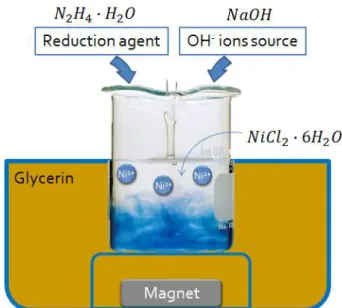
Figure3.1: Schematic for the hydrothermal process with a teflon beaker involved by glycerine and placed above a fixed magnet.
In both cases after adding NaOH, the teflon beaker was transferred to a hot bath at the desired temperature allowing us to place a magnet below it as described in [15] in order to create a fixed magnetic field measured with a teslameter. The intensity of this field was approximately 15mT 3cm above the magnet, height in which the solution was set so that the reaction could occur and this arrangement is shown in figure3.1.
3.2
Electrochemical synthesis
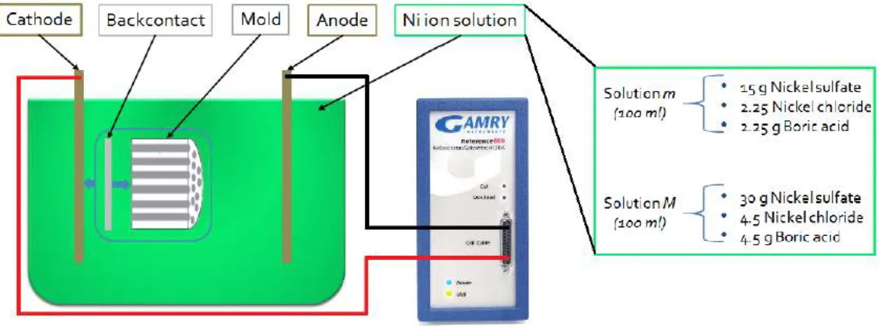
At some point it was decided to produce the nanowires through an electrochemical method that was presented as promising and more feasible. For this it was necessary a template where nanowires would form, a nickel ion solution, that was always the same in all electrodepositions made throughout this work, an anode and a cathode. The solution was produced with nickel sulphate, nickel chloride and boric acid. These were mixed in two different ways to produce solutions with two distinct concentrations as presented on the right side of figure 3.2. This was made initially with 1.5V batteries and copper electrodes which is a very easy and simple way to do it, but does not allow much control over the process variables. This arrangement was then changed to an electrolytic cell attached to a GamryReference 600 potentiostat as illustrated in figure 3.2which would
allow to control the current/voltage applied and the distance between electrodes. At first it was made a test on plain gold film with a titanium layer for adhesion on a glass substrate, deposited by e-beam deposition. This process was carried out without any template using different electrolyte concentrations (solutionsmandM), applied currents (1V and 3V) or voltages (1mA and 5mA) with a duration of 20min for each sample.
3.2. ELECTROCHEMICAL SYNTHESIS
Figure 3.2: Schmatic for the electorchemical method used to produce nickel structures (left) and also showing both solutions used (right).
3.2.1 Alumina membrane
Ina firststageanodizedaluminatemplateswereusedwitharound200nmofpore diameterandathicknessofapproximately70µmfromWhatman,followingthestepsof Bentleyetalin[1].Theprocesswasmadewithanappliedcurrentof25mAfor2hoursdue toafirstparameterstestanalysedinthenextchapter,withagoldbackcontact60nmthick anda10nmtitaniumlayerforadhesionbetweenitandthetemplateonthemembrane depositedbye-beamdeposition,beingthisideatakenfrom[11].Thetemplatewasfixed with thegold side facingthe cathode as illustratedinfigure 3.2and a nickelfilament asanode1cmapartsubmergedinsolutionM.Afterthedeposition ,themembranewas etchedwithanNaOHsolution(6mol/L)and the product dispersedinIsopropylalcohol (IPA). This process was also attempted with a platinum backcontact 70nm thick with exactlythesamearrangementasbefore.
3.2.2 Wax mold
Anotherdirectiontowardsmorelowcostmaterialsturnedustowaxpatternstoreplace thealuminatemplate.TheseweremadewithaXeroxwaxinkprinterinapolyethylene naphthalate (PEN) substrate with a 60nm gold film and a 10nm titanium layer for adhesion ,both depositedbye-beamdeposition.Inthis processwas usedPEN dueto hisflexibility,whichwasnecessary forthe printingprocess. Theprintingsweremade in photo mode to achieve greater thickness (around 12µm). The patterns consistedof a black rectangle (1cm by 3cm) with several square holes within with 250µm side length designedinadobeillustrator.This designallowedusto printholeswitharound100µm widewiththewaxinthesubstrate.
CHAPTER 3. MATERIALS AND METHODS
After a parameters test the electrodepositions were carried out using theMsolution, 1cm between electrodes and an applied current of 100µA for around 4 hours. Then the samples would be submerged in acetone, applying ultrasounds if necessary, in order to remove the wax pattern, leaving the nickel structures on the substrate to be characterized by profilometry and optical microscopy.
3.2.3 Polydimethylsiloxane (PDMS)
After using wax it seemed that PDMS could have some role to play in these processes, so this material was investigated and patterned by laser. The laser was set with a height of 5cm above the PDMS sample, with a power of 100% and a speed of 10% in order to cut a pattern previously designed in adobe illustrator that consisted on a single hole with 500µm of diameter.
3.2.4 Epoxi-based photoresist (SU-8)
Forlastinthiswork SU-8wastested asreplacement formoldmaterial due tohis highsensibilitytoanelectronbeamallowingpatterningbye-beamlithography.Soitwas depositeda7µmthickfilmofthismaterialbythestandardspin-bakingprocesswherethe SU-8wasspunat900rpmfor30secondsandheatedthroughheatrampsof2°C/minuntil itreached65°Cwhereitstoodfor10minutesandagainuntil95°Catthesameratewhere itwasheldforanother10minutes.Afterthisitwaslettocooldownatroomtemperature. Thismaterialwasspunontopofgold/titaniumcoveredglasssubstratessimilartothose previouslyreferred.
Topatternthese filmssomeweresubmittedtoastandardphotolithographicprocess wheretheywereexposedthroughapre-designedmechanicmaskwithapredefineddose andsubmittedtoapre-exposurebaking.
Othersampleswerepatternedwithe-beamlithographywheredifferentscenarioswere testedforpixelsize,acceleratingvoltageanddose.Thepixelsizevariedbetween0.1and1 µm,thedoseswentfrom1to8µC/cm2 andvoltagesfrom10to30kV.Afterexposure, the sampleswerebakedfor10minutesat65°Candlettocooldownatroomtemperature. ThentheyweredevelopedwithanSU-8developermainlycomposedofPropyleneGlycol MonomethylEtherAcetate(PGMEA)foraround30seconds,rinsedwithIPAanddried withannitrogenairgun.
Finally, the samples that could be used in electrodeposition were included in the electrolytic cell arrangement described in sections above with an applied current of 25mA for 1 hour and then submerged in a stripper (TechniStripP1316) solution for 1 hour and 20 minutes in order to strip SU-8 material and leave the nickel structures on the substrate. This was made in an ultrasonic bath to completely remove the stripped material. After this process, samples were rinsed with IPA and dried with a nitrogen air gun.
3.3. CHARACTERIZATION
3.3
Characterization
In this work weused several methods to characterize the structures produced on differentsynthesis.Forthemorphologicanalysisitwasusedopticalmicroscopywith an
Olympus BX5 1 and scanning electron microscopy with a Zeiss Auriga CrossBeam
Workstation. To characterize the topography of the samples we used profilometry
analysis with an Ambios XP-Plus 2 0 0 Stylus and also toanalysethesurfaceandthickness/ height of the produced structures. For a structural and elemental analysis it was performed X-ray diffraction in a PANalytical XPert PRO and Energy-dispersive X-ray spectroscopy in an Oxford X-max 1 5 0 detector with AzTec software (inside Zeiss Auriga).
Chapter 4
Results and discussion
This work, as it was mentioned before, started with solution based production methods due to their low cost and process conditions as low temperature. In this stage several synthesis were attempted and in this chapter all results will be analysed and characterized.
4.1
Synthesis of nickel structures by hydrothermal method
The first results were obtained without an applied magnetic field, which is often referred to, but also the most difficult component to control in this process. This showed us what would be the result of this process without the influence of the magnetic field and therefore allowed us to understand the growth mecanism of these structures.
4.1.1 Without magnetic field
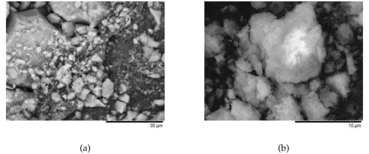
In the first synthesis method mentioned in the previous chapter, temperature was applied at the beginning of the process, since previous trials with temperature only in the second part (after the addition of NaOH) didn’t reveal any significant results. With the process as it was described, nickel particles were obtained and dispersed in solution, which were evaluated by scanning electron microscopy (SEM) as shown in figure 4.1a.
(a) (b)
Figure 4.1: Morphology analysis by SEM of nickel particles obtained by hydrothermal method with nickel sulphate hexahydrate (a) and with nickel chloride (b).
CHAPTER 4. RESULTS AND DISCUSSION
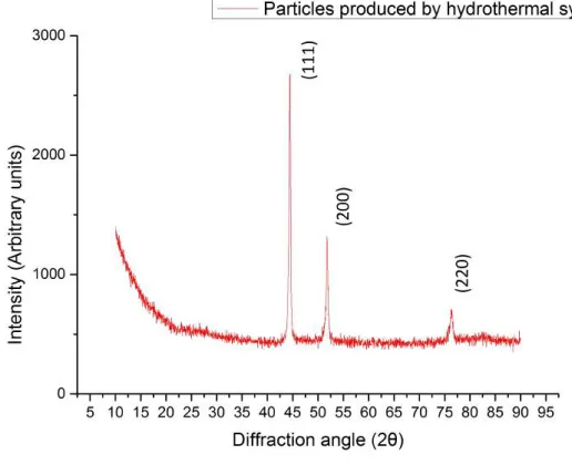
Then a different reagent combination was tried, but with the same result, visible in figure4.1b. Both cases produced nickel particles not because of the reagents, proportion, temperature applied or reaction time, but due to the lack of a magnetic field. These particles where analyzed by X-ray diffraction (XRD), resulting in the plot present in figure 4.2where it is possible to observe three peaks related to the planes (111), (200) and (220), reflecting a face-centered cubic (fcc) phase nickel, which are in agreement with the values in the Joint Committee on Powder Diffraction Standards (JCPDS) card no. 45-1027 [2].
Figure 4.2: XRD pattern of Nickel particles synthesized by hydrothermal method showing fcc phase nickel peaks.
4.1.2 With magnetic field
After this, the process was set in a hot bath with a magnetic field as described in the previous chapter, but unfortunately the magnets at our disposal were not as stable as those used in literature apparently, working only after several attempts and with no reproducibility whatsoever. However, it is true that it could produce nanowires, the successful synthesis resulted in a very small quantity of these structures dispersed in Isopropyl alcohol (IPA).
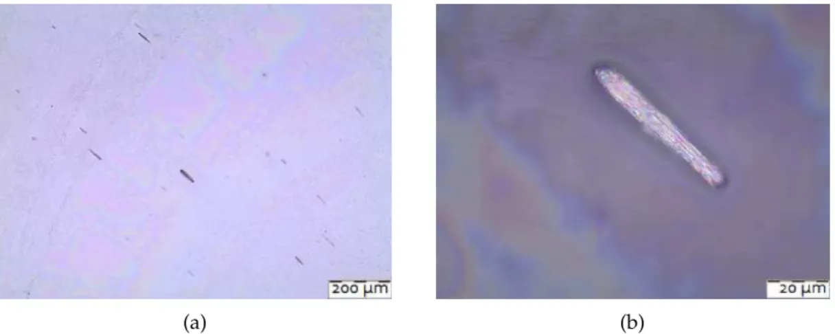
Theresultsareshowninfigure4.3a whereispossibletoverifythesmallquantityof nanowires,butaverygoodaspectratiowithverydifferentlengthsgoingfromalmost10 to 70microns, measured in the optical microscope. In the first figure is also presented a
propertynoticeableevenwhenthese
4.1. SYNTHESIS OF NICKEL STRUCTURES BY HYDROTHERMAL METHOD
(a) (b)
Figure4.3:Opticalmicroscopyanalysisofnickelnanowiresobtainedbyhydrothermal methoddispersedinIPAanddropcastedinaglasssubstrate. (b) is a magnified region of oneofthese aggregates.
property noticeable even when these structures are in solution that is it reaction to an external magnetic field after the synthesis process. This could be observed with them dispersedandinthesampleformicroscopeobservationpreparedonahotplatewitha fixed magnetic field from the agitator, in this case the nanowires aligned themselves withthisfield,showingapreferredorientation.
AfterSEManalysisit was possibletosee themorphology ofthesestructures and, as shownin figure 4.4, they arecomposed bybeads and presenting,as said before,a goodaspectratiowithwidthsaround800nm,valuemeasuredwithimagejsoftware.
Figure 4.4: Morphology analysis by SEM of nickel nanowires obtained by hydrothermal method with magnetic field, showing a bead composition observable in the magnified area (b).
This method could be used for nanowire production, but it would be necessary an optimization in the magnetic field component with more accurate and stable magnets or maybe a different arrangement in order to have a stable and controlled process.
CHAPTER 4. RESULTS AND DISCUSSION
4.2
Synthesis by electrochemical method
Withthefirstassemblydescribedandshownwithamoldinthematerialsandmethods
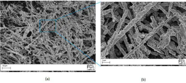
chapter,whereitwasusedanaluminamembranewithasetofbatteriestoapplyvoltage for the electrodeposition, it was possible to understand how this process works. In this process it was producednickelnanowires visiblein SEM samples as shown in figure 4.5 with widths close to 200 nm, measured by imagej. These are also shown in figure 4.6a thatatfirstseemlikethickstructureswithaverylowaspectratio,butifwelookcloser infigure4.6b,itisclearthattheyareinfactverythinnanowires,butallaggregatedin groups. It was also possible to notice a reaction from these structures to an external magneticfieldalsoobservedinsamplesanalysedpreviously.
Figure 4.5: Morphology analysis by SEM of nickel nanowires obtained by electrochemical method with an alumina membrane and batteries as voltage source.
As this process showed a very low yield it wasn’t possible to obtain a great amount of material. For this reason it was necessary to use a more controlled process and to optimize the membrane backcontact because one of the causes for this low efficiency was the unused part of the membrane (around 80%) due to low conductivity in that area.
4.2. SYNTHESIS BY ELECTROCHEMICAL METHOD
(a) (b)
Figure 4.6: Optical microscopy analysis of nickel nanowires obtained by electrochemical method with an alumina membrane and batteries as voltage source dispersed in IPA and dropcasted in a glass substrate with a magnification on the centre aggregate (b).
It was then decided to use a potentiostat as current/voltage source. At first it was made a parameters test with no template to analyse the influence of variables in the film thickness. The plots presented in figures4.7aand4.7bshow the results of this test.
(a) (b)
Figure 4.7: Plots of Applied voltage vs final thickness (a) and Applied current vs final thickness (b) of nickel films deposited on samples of gold and titanium on glass substrate using two different solution concentrations.
With these it was possible to see that for the values range proposed for the experiments the use of voltage would be preferable instead of current. However, as this process depends on current density and because the electrode area stays the same through the deposition it was decided to apply a constant current, but with a higher value in order to reach a reasonable thickness, being this approximately 25mA. It was also possible to see that for greater thickness the electrolyte concentration starts to make difference and therefore solutionMwas chosen to be used in future electrodepositions.
4.2.1 Alumina membrane
CHAPTER 4. RESULTS AND DISCUSSION
As the alumina membranes were used in the previous test and said to reveal a low yield, some samples were covered with two different materials in the back by e-beam deposition in order to optimize the backcontact. In some it was deposited a film of platinum and in others gold with titanium. This way the electrodeposition process showed a higher yield using all the membrane.
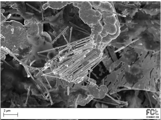
Figure 4.8: Morphology analysis by SEM of nickel nanowires obtained by electrochemical method with platinum backcontact on an alumina membrane, where it is possible to see the platinum fragments (b) with several nanowires on top (a).
However, in both cases the backcontact was a problem after etching the membrane as it would not separate completely from the resulting nanowires, being this perceptible in figure4.8. This would be the reason in this sample for the lack of reaction to an external magnetic field due to the remaining platinum that would prevent nickel structures from move and align with the field. However, some nanowires could be seen in solution showing widths of 200 nm due to the well defined pores in the template and with lengths between 40 and 70 microns.
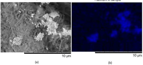
Figure 4.9: Element analysis by SEM-EDS of platinum on nickel nanowires sample obtained by electrochemical method with platinum backcontact on an alumina membrane, where it is possible to see the platinum fragments in blue (b).
4.2. SYNTHESIS BY ELECTROCHEMICAL METHOD
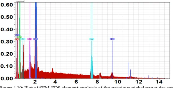
This platinum presence was verified with an Energy-dispersive X-ray spectroscopy (EDS) analysis shown in figure4.9where it is perfectly visible the fragment composition in blue identifying the platinum element and in figure4.10where is described all the SEM image elements with platinum, nickel from the nanowires, aluminium and oxygen from traces of the membrane and carbon from the backplane.
Figure 4.10: Plot of SEM-EDS element analysis of the previous nickel nanowire sample presented in figure4.9.
Figure 4.11: Optical microscopy analysis of nickel nanowires obtained by electrochemical method with gold backcontact on an alumina membrane, dispersed in IPA and dropcasted in a glass substrate.
In the case of the gold back-contact, several chemicals were used in the attempt to remove this material, butinthe end the onlymethodthatmadeanyeffect wasthemechanicaletching,more properly,smoothlyscratchingthe surface until gold disappeared. Thiswayitwaspossibletoobtain nanowiresisolatedfromthe back-contact,butnotfromthemselves astheywouldnotdispersein solu-tion, formingaggregates.Thiscan beseeninfigure4.11.
These structures presented same widths as those obtained with a platinum contact and a
very regular shape as shown in figure 4.12, but this time with very constant lengths close to 60 microns measured by optical microscopy.
CHAPTER 4. RESULTS AND DISCUSSION
Figure 4.12: Morphology analysis by SEM of nickel nanowires obtained by electrochemical method with gold backcontact on an alumina membrane, showing a mean width of 200 nm and a very regular shape.
It was also observed a property that was expected in view of the previous results and that was a reaction to an external magnetic field, being this explicit in figure4.13where it is clear that the nanowires dispersed in solution starts reacting to the field lines, following them until they reach the glass that is against the magnet and accumulate all the material in that region.
Figure 4.13: External magnetic field effect on nickel nanowires in solution, obtained by electrochemicalmethodwithanaluminamembrane.
4.2.2 Wax mold
At this time we turned to more low-cost approaches, more properly, cheapest and easier to work on alternative materials for the alumina membrane. In this line of thought came the wax masks on polyethylene naphthalate (PEN) flexible substrate as printable substitute. First it was investigated what would be the most suitable print mode for this process given that it would have the ultimate aim of production structures with high
4.2. SYNTHESIS BY ELECTROCHEMICAL METHOD
aspect ratio. It would therefore be important to get thick wax layer. For this, normal and photo mode were compared to which were obtained layers about 8 and 12 microns thick respectively.
(a) (b)
Figure 4.14: Optical microscopy analysis of holes printed with wax on PEN with gold substrates from designs with 500µm circles (a) and 250µm circles (b) resulting in approxi-mately 400µm and 150µm widths respectively.
Taking into account the options, photo mode was chosen to be used hereinafter and it was considered the hypothesis of overprinting the pattern, but given the design character-istics would be near impossible to successfully carry out the layers alignment. The next step was to study the resolution of this method.
In order to do this it was decided to start with circular holes on the wax surface. Therefore several samples were made with different hole widths as shown in figures4.14a,
4.14band4.15.
(a) (b)
Figure 4.15: Optical microscopy analysis of holes printed with wax on PEN with gold substrates from a design with 125µm circles resulting in around 40µm widths (a), however, showing some randomness in the pattern (b).
The first ones (figure4.14a) were designed with a 500 microns width resulting in a real distance of about 400µm. Then this value was reduced by half (figure4.14b), resulting in features with widths around 150 microns, but no characteristic geometry. The last figures,4.15band4.15a, both represent the same holes and in the right one we can verify a
CHAPTER 4. RESULTS AND DISCUSSION
randomness when we got to this scale. On the left it is noticeable that for these circles with 125 microns in the drawing the dimension has been reduce like in all the other examples, ending with around 40 microns wide, also losing any geometry.
After observing the loss of geometry in previous features and analysing the printing characteristics it was decided that it might be best if the holes were square instead of circular. Then were made new designs with the same dimensions as the previous ones, but with that change in geometry.
(a) (b)
Figure 4.16: Optical microscopy analysis of holes printed with wax on PEN with gold substrates from designs with 500µm squares resulting in approximately 400µm widths (a) and from 125µm squares showing some randomness in the pattern (b).
It was observed that for the features with 500µm and 250µm, represented in figures
4.16aand4.17a, the results were very similar in dimensions when compared to the ones
with circular design, but with fewer geometric loss. In case of the 125µm design, it results in a pattern with a little bit more resolution, but yet with some randomness that would make a big part of the template unusable as it can be observed in figure4.16b.
(a) (b)
Figure 4.17: Optical microscopy analysis of holes printed with wax on PEN with gold substrates from a design with 250µm squares resulting in around 150µm widths (a), reduced to 100µm when affected by proximity (b).
However, when designed with a smaller inter-hole distance the features start to affect each other with a proximity effect, reducing the hole widths from around 150µm to 100µm
4.2. SYNTHESIS BY ELECTROCHEMICAL METHOD
and this is visible in figure4.17b.
With all these tests it was decided to use hereafter a pattern with 250µm side squares close to each other to promote the proximity effect, which were printed on photographic mode on top of a PEN substrate covered with titanium and gold as described in the previous chapter.
Then these samples proceeded for the electrodeposition process and for this was necessary a study of parameters since these would have different effects in the presence of a wax template attached to the cathode. This way it was possible to have an idea of how long or how much current should be applied in order to get a specific thickness.
Applied current (µA) Reaction time (minutes) 5
20
100 60
120 180
Table 4.1: Parameters chosen to study the time influence in nickel structures produced by electrochemical method on samples of wax molds on top of gold covered PEN substrates.
Reaction time (minutes) Applied current (µA)
5 25 50 60 75 100 150
Table 4.2: Parameters chosen to study the current influence in nickel structures produced by electrochemical method on samples of wax molds on top of gold covered PEN substrates.
To perform this, the study was divided in two parts, time and current influence. Several samples were subjected to an electroplating process under the conditions defined in tables 4.1and4.2and subsequently analysed by profilometry to determine the thickness of the created structures. With this mold material was necessary lower current values to prevent damaging the templates during the electrodeposition process.
CHAPTER 4. RESULTS AND DISCUSSION
(a) (b)
Figure 4.18: Plots of time vs final thickness (a) and current vs final thickness (b) of nickel structures produced by electrochemical method on samples of wax molds on top of gold covered PEN substrates.
Withthisinformationweobtainedthegraphs4.18a and4.18b whereitwaspossibleto checktheincreaseinthisthicknesswithreactiontime,however,thesamplerelatedtothe smallesttimeprovedinconclusiveand is thusnotrepresented.
It was also verified that for longer times the wax mold began to show some damage compromising the patterning making impossible its subsequent analysis. In the case of applied current, the initial sample also proved inconclusive and it was also observed that this material would peel off from the substrate for higher current values.
(a) (b)
Figure 4.19: Optical microscopy analysis of nickel structures obtained by electrochemical method with a wax mold on top of gold covered PEN substrates.
Thereafter we proceeded with the electrodeposition process which used an assembly equivalent to those described above where the gold on the substrate also served as cathode. This was done with a current of 100µA for 4 hours, resulting in the structures presented in figure4.19after wax removal with acetone.
Afteraperfilometry analysis, wecouldobserve widthsclose 100 micronsashad the waxpattern,butatthesametimesomediscrepanciesregardingtheheightofthestructures, presentingverydisparatevalues.Thesereflectacertainirregularityindepositedfilms whichwasthoughttoberelatedtothefactofbeingusedanappliedcurrentinsteadof voltage,butthisidea wasdiscardedwithadditionaltests.Ormayberelatedtoa local anomaly,whichhasbeenfoundtobewrongafteranalysisofotherareasofthesample.
4.2. SYNTHESIS BY ELECTROCHEMICAL METHOD
Thus, for now, the cause for this is unknown, it may be related to various factors such as the electrolyte used, the assembly itself or even the electrical properties of the electrodes.
Looking now in a slightly more general point of view it is therefore possible to create coherent structures using this technique with some optimization, but these do not have the aspect ratio desired for the primary purpose of this work and could not be subsequently used to produce transparent conductive films. However these results should not be taken lightly and could be very useful for applications such as inter-layer contacts using simple processes or even as templates for micro-fabrication processes.
4.2.3 Polydimethylsiloxane (PDMS) and parylene
After testing with wax some alternative materials were considered such as parylene which proved unsuitable due to the need of large quantities of material to produce films with acceptable thickness, i.e., in the order of tens of microns and for this reason it was discarded.
AnotherpossibilitywouldbeamaterialcalledPDMS.Inaplainsampleofabout2mm thicknessitweretestedseveralcasestostudythepatterningofthismaterialusingalaser printer,ascanbeseeninfigure4.20.Withthisitwaspossibletofindoutwhatwasthe smallestwidththatcouldbeachievedwhenpatterningholes,thisbeing around 400µm.
Figure 4.20: PDMS disc after patterning by laser printing.
However, in the first attempts the obtained features had a conical geometry wider in the upper face but with some parameters optimization it could be more cylindrical as shown in figure4.21in which it can be seen that the widths observed in upper and lower faces were very similar. However, even with this study, this idea has not continued for electrodeposition not only because of possible difficulties depositing this material in gold, but mostly due to problems that would arise during the removal, i.e., in the etching process. This because the PDMS has a high resistance to chemicals and mechanical erosion
CHAPTER 4. RESULTS AND DISCUSSION
(a) (b)
Figure 4.21: Optical microscopy analysis of PDMS disc after patterning by laser after parameter optimization,showing the upper face in (a) and the lower face in (b) both with identical dimensions.
would not be viable for the structures we wanted to produce. For these reasons it was also discarded as possible replacement.
4.2.4 Epoxi-based photoresist (SU-8)
FinallyinthisworkwestudiedSU-8asanalternativematerial.Asreferredinmaterials andmethodsseveralsampleswereproducedwiththistobepatterned.First, thesewere used inan e-beam lithography (ebl) process inwhichmultiple exposureswere made inordertoevaluatethe effectofvariables,followingthevaluesinthetable4.3,repeating thepatternseeninfigure4.22a foreachexposure.
After exposure, baking and development samples were observed in an optical micro-scope and characterized in a profilometer.
(a) (b)
Figure 4.22: Pattern used in e-beam lithography of SU-8 on top of gold covered glass samples, as introduced in the imaging software (a) and after transferred to the material, analysed by optical microscopy (b).
The profilometry measurements on these samples were performed in the same place, with the same orientation and direction as the red vector present in figure4.22b.
4.2. SYNTHESIS BY ELECTROCHEMICAL METHOD
Table 4.3: Design of experiment for e-beam lithography of SU-8 on top of gold covered glass samples.
Accelerating voltage (kV) Dose (µC/cm2)
Pixel size (µm) 10 1 1 2 4 8 20 1 1 2 4 0.5 8 0.1 30 1 1 2 4 8
The samples exposed at 10 kV were all impossible to analyse as can be seen in figure
4.23adue to the development step, with this being probably due to the short development
time. For 20 kV we can see that a pattern was retained, visible in figure4.23b, but also that it was not the only thing to stay in the sample. The outer rectangle is also crosslinked and this comes from the SEM image window in which the lithography procedure was done.
(a) (b)
Figure 4.23: Optical microscopy analysis of SU-8 samples after e-beam lithography process with 10kv (a) and 20kV (b) of accelerating voltage.
This can be confirmed by profilometry analysis shown in the figure 4.24 where it is noticeable the shape of the lines transferred to the SU-8 on the surface, but also the presence of all the remaining surrounding material with approximately the same thickness as estimated for the film deposited at first. This phenomenon was due to an anomaly in the e-beam lithography process from the rendering software that, after performing the pattern exposure, showed one image frame of the sample through the SEM briefly exposing the entire material visible on that window. Therefore, as the SU-8 is a very sensitive material,
CHAPTER 4. RESULTS AND DISCUSSION
this time was sufficient to crosslink most of the depth of the resulting film structure that can be seen in figure4.23b.
Figure 4.24: Thickness of one SU-8 sample prepared by e-beam lithography with a 20 kV accelerating voltage analysed by profilometry.
Apart from this problem the best results of this study were with 30 kV acceleration since the samples with different pixel sizes showed no conclusive result as can be seen in figures
4.25aand4.25bwhere the first has no significant pattern and the second one has lines 20
nm high that is bellow the equipment resolution. In the case of 30 kV were observed higher definition, decreasing with the applied dose as can be seen by comparing the figures4.26a
and4.26bwith 1 uC/cm2and 4 uC/cm2respectively as well as a deformation of the whole
surface.
(a) (b)
Figure 4.25: Surface profilometry analysis of SU-8 samples prepared by e-beam lithography with a pixel sizes of 0.1µm (a) and 0.5µm (b).
Through this analysis it was concluded that the best conditions were 30 kV acceleration,
4.2. SYNTHESIS BY ELECTROCHEMICAL METHOD
1 uC/cm2 dose and a pixel size of 1 µm. However, in order to apply this in future applications it is necessary to solve the software problem, otherwise it is not possible to produce usable molds.
(a) (b)
Figure 4.26: Thickness of SU-8 samples prepared by e-beam lithography with a 20 kV accelerating voltage and different doses, 1 µC/cm2 (a) and 4 µC/cm2 (b) analysed by profilometry.
This material was further tested with a normal process of photolithography and after development we obtained features with a definable minimum width of around 5µm as shown in figure4.27, being the pattern fully-defined until it reaches the gold contact under the film.
Figure 4.27: Optical microscopy analysis of an SU-8 sample after standard photolithog-raphy process on gold covered glass substrates, showing the narrower feature with approximately 5µm.
It is possible to see this in figure4.28corresponding to the profile analysis of a hole with greater width because the profilometer needle was not able to reach the gold in the
CHAPTER 4. RESULTS AND DISCUSSION
first case due to its diameter, which is higher than 5 µm. Thus it is also possible to check the thickness of the SU-8 film which corresponds to its estimated value.
Figure 4.28: Thickness of SU-8 samples prepared by standard photolithography on gold covered glass substrates, analysed by profilometry.
Figure 4.29: Schematic for the sample used in the stripping test.
With these samples was then possible to proceed with the electrodeposition which followed the same assembly as the previous ones, with 25 mA of applied current for 1 hour. These samples were then subjected to an etching process for which there was conducted a test with a glass samples with titanium, gold and nickel, as illustrated in figure4.29, in order to determine if this process affect the materials present in the samples to be treated after electrodeposition. For this it was submerged in a stripper solution at 65°C for 2 hours, taking photos at every 10 minutes as can be seen in figure4.30.
Figure 4.30: Test sample (showed in figure 4.29) during the stripping process, with pictures taken every 10 minutes.
4.2. SYNTHESIS BY ELECTROCHEMICAL METHOD
In this test it could be seen that in about 90 minutes almost all of the gold present in the sample was removed, leaving just the nickel and titanium. This has proved useful because during the SU-8 etching process it also removes the gold, leaving only the nickel structures.
Figure 4.31: Stripping process of one sample made by standard photolithogtaphy observed every 15 minutes, showing the nickel structures that remained in the substrate in the end of the process (bottom right).
After electrodeposition these samples underwent in this process, being necessary to use an ultrasonic bath in order to detach the SU-8 film while it was being stripped. At the end of this procedure the smallest structures peeled off due to these ultrasounds while the others remained on the substrate as shown in figure 4.31. This ultrasonic bath was necessary because the SU-8 template wasn't dissolved by the stripper, but swelled and this is can be avoided with different stripping solutions.
Chapter 5
Conclusion
With this work it was possible to study several methods to produce nickel nanowires, from hydrothermal methods to electroplating based processes. Of all the methods, those that showed better results were the electrochemical ones since they used molds with very well defined nanosized features. These allowed us to obtain nanowires 200 nm wide and around 60 micrometers long, presenting a great aspect ratio. Although, this was only possible due to a controlled source that delivered a steady and constant current in the deposition step. However, this method could be improved if one of the final stages was optimized, being this the backcontact etching. The gold contact used in the samples was very hard to etch since several acids did not work, leading to a very careful and superficial mechanic etching in order to obtain isolated nanowires, otherwise these would stick to the back contact and it was not possible to disperse them in solution. In the future it would be interesting to try this step with aTechniStripP1316 solution since it was showed that it could dissolve the gold, leaving only the nickel.
Even with all the nanowires produced and isolated from the backcontact it is also necessary to study their dispersion in solution in order to solve the constant aggregation present in the samples, being this via reagent addition or even by different transfer method when transderref to a substrate since the samples were made by dropcasting.
For this method the only template that resulted in usable features was the anodized alumina membrane, while all the other alternative materials revealed to be able to produce only low aspect ratio structures. In the case of SU-8, it could be used to produce these structures if a dedicated e-beam lithography was used in order to prevent bulk crosslinking and also after optimizing the stripping step, using a different solution to dissolve the mold instead of swell it. However, even not being applicable for the main objective of this work, the structures obtained with other mold could be explored in the future for applications that does not demand a high aspect ratio, such as interlayer connectivity in integrated circuits with low cost processes.
In the other hand, hydrothermal methods studied also resulted in very good nanowires even though there was a very wide range for the length of these structures a very irregular structure (bead composed nanowires). Although showing widths of 800 nm, the length suffered from what has been said, being the reason for this the instability of the applied magnetic field. In the future would also be interesting to study this methods with different configurations for the magnets, such as a side-to-side arrangement instead a bottom one or even between coils to generate a magnetic field in the centre where would be the solution.
In both cases the nanowires produced showed a very interesting magnetic response,
CHAPTER 5. CONCLUSION
being this already used in the cleaning step of the mold based method, where through a magnetic field it was possible to separate these structures from the remaining material. This characteristic could be far more explored in the transparent conductive films, allowing to create an organized network of these structures with an applied magnetic field to promote nanowire alignment.
In conclusion these methods are very useful for nickel nanowire production with the optimizations yet to be made in the referred steps in order to apply these structures in transfer methods to produce nanowire networks and move on to the next stage in the production of transparent conductive films based in nickel nanowire networks. And also that the alternative materials studied can be used in production of structures to be applied in interlayer connections or templates for micro-fabrication processes.
![Figure 2.2: Illustration of electrochemical synthesis steps until obtain free nickel nanowires, adapted from [1]](https://thumb-eu.123doks.com/thumbv2/123dok_br/16693238.743721/27.892.393.789.191.434/figure-illustration-electrochemical-synthesis-obtain-nickel-nanowires-adapted.webp)