AIP Conference Proceedings 1646, 106 (2015); https://doi.org/10.1063/1.4908590 1646, 106 © 2015 AIP Publishing LLC.
Potential up-scaling of inkjet-printed devices
for logical circuits in flexible electronics
Cite as: AIP Conference Proceedings 1646, 106 (2015); https://doi.org/10.1063/1.4908590 Published Online: 19 February 2015
Kalyan Yoti Mitra, Enrico Sowade, Carme Martínez-Domingo, Eloi Ramon, Jordi Carrabina, Henrique Leonel Gomes, and Reinhard R. Baumann
ARTICLES YOU MAY BE INTERESTED IN
Flexible hybrid circuit fully inkjet-printed: Surface mount devices assembled by silver nanoparticles-based inkjet ink
Journal of Applied Physics 121, 104904 (2017); https://doi.org/10.1063/1.4977961 Fully inkjet printed flexible resistive memory
Applied Physics Letters 110, 143503 (2017); https://doi.org/10.1063/1.4978664
Effect of the light spectrum of various substrates for inkjet printed conductive structures sintered with intense pulsed light
Potential Up-scaling of Inkjet-Printed Devices for Logical
Circuits in Flexible Electronics
Kalyan Yoti Mitra
1, a), Enrico Sowade
1, b), Carme Martínez-Domingo
2, 3, c), Eloi
Ramon
2, 3, 4, d), Jordi Carrabina
2, e), Henrique Leonel Gomes
6, f), Reinhard R.
Baumann
1, 5, g)1Technische Universität Chemnitz, Department of Digital Printing and Imaging Technology, Chemnitz, Germany 2Printed Microelectronics Group, CAIAC,Universitat Autònoma de Barcelona, Bellaterra, Spain 3Nanobioelectronics & Biosensors Group, Catalan Institute of Nanotechnology (ICN), Universitat Autònoma de
Barcelona, Bellaterra, Catalonia, Spain
4Institut de Microelectrònica de Barcelona, IMB-CNM (CSIC), Bellaterra, Catalonia, Spain
5Fraunhofer Institute for Electronic Nano Systems (ENAS), Department of Printed Functionalities, Chemnitz,
Germany
6Universidade do Algarve, Institute of Telecommunications, Faro, Portugal
a)[email protected] b)[email protected] c)[email protected] d)[email protected] e)[email protected] f)[email protected] g)[email protected]
Abstract Inkjet Technology is often mis-believed to be a deposition/patterning technology which is not meant for high
fabrication throughput in the field of printed and flexible electronics. In this work, we report on the 1) printing, 2) fabrication yield and 3) characterization of exemplary simple devices e.g. capacitors, organic transistors etc. which are the basic building blocks for logical circuits. For this purpose, printing is performed first with a Proof of concept Inkjet printing system Dimatix Material Printer 2831 (DMP 2831) using 10 pL small print-heads and then with Dimatix Material Printer 3000 (DMP 3000) using 35 pL industrial print-heads (from Fujifilm Dimatix). Printing at DMP 3000 using industrial print-heads (in Sheet-to-sheet) paves the path towards industrialization which can be defined by printing in Roll-to-Roll format using industrial print-heads. This pavement can be termed as “Bridging Platform”. This transfer to “Bridging Platform” from 10 pL small print-heads to 35 pL industrial print-heads help the inkjet-printed devices to evolve on the basis of functionality and also in form of up-scaled quantities. The high printed quantities and yield of inkjet-printed devices justify the deposition reliability and potential to print circuits. This reliability is very much desired when it comes to printing of circuits e.g. inverters, ring oscillator and any other planned complex logical circuits which require devices e.g. organic transistors which needs to get connected in different staged levels. Also, the up-scaled inkjet-printed devices are characterized and they reflect a domain under which they can work to their optimal status. This status is much wanted for predicting the real device functionality and integration of them into a planned circuit.
INTRODUCTION
Inkjet technology finds it use in a wide variety of precision applications. It is a renowned, but yet an adaptable additive technology for depositing precious functional electronic materials. One of such applications is the inkjet printing of electronic devices and circuits. Recently, many research papers have been published which have involved inkjet technology for fabricating the electronic devices and circuits such as organic thin film transistors and
capacitors for various applications [1-11]. These applications have been either aimed for optimizing of the individual electronic device or for integration towards fabricating an electronic circuit operating for a specific purpose [1-12]. But, very less focus has been concentrated on the fabrication yield of the electronic devices and possible circuitry. Especially in case of electronic circuits where different electronics devices are connected in defined arrangement, the stability of a deposition technology becomes very important [10-11].
In most of the researches, laboratory desktop inkjet printers are used for fabricating electronic devices using either conventional or un-conventional functional inks. Here, this kind of the printing stage where proof of concept devices is manufactured not for high yield is termed as “Laboratory Platform”. It is noted that these printers have many constraints which do not allow the electronic devices to show high fabrication yield and characteristic performance. Shown below in Fig. 1 (a), (b) and (c) are the printing defects for Source/Drain electrodes (thickening of the inter-digitated Source/Drain finger causing short circuit) and layer in-homogenities in case of dielectrics (ripple formation). These defects are caused either due to the ejected drop instability or the usages of the limited number of jetting nozzles at par with the fast evaporation of the solvent from the deposited ink layer. It can be concluded that this deposition platform is not suitable where the primary requirements are high deposition speed and stability; and also homogeneity in the interfacial layers at the multi-layered stack for electronic devices.
(a)
(b)
(c)
FIGURE 1. Microscopic image of (a) short circuits between the Source/Drain electrodes; and microscopic image of in-homogeneities over the printed layer for (b) dielectric ink no.1, (c) dielectric ink no.2
On the contrary, “Bridging Platform” refers to an intermediate up-scaled deposition stage where the industrial print-heads are used for a Sheet-to-Sheet manufacturing platform. This up-scaling process can be explained by the usage of large number of nozzles and also the drop volume related to the industrial print-head used while printing. All the deposition parameters which are used in this Bridging Platform can be furthermore used and transferred when printing on Roll-to-Roll manufacturing platform (based on Inkjet Technology). This Bridging Platform can also be defined as the evaluation stage for an industrialized manufacturing process, where relatively huge numbers of electronic devices are printed with moderate speed and these devices are afterwards tested for the characteristic performance with respect to the fabrication yield obtained. From the results, it can also be predicted if this Bridging platform is suitable for fabricating electronic logical circuits. Herein, we demonstrate the concept of Bridging Platform with the experimental setup which shows the characterization results obtained for the various inkjet-printed devices.
MATERIALS AND METHODS
Following methodology and materials were adapted for accomplishing the printing of different electronic devices on the A4 sized (210 mm × 297 mm) polymeric foil.
Materials
Three basic functional inks were used for printing the different electronics devices. Exemplary a) silver nano-particle ink (SunTronic EMD 5603 from SunChemical) was used for printing the conductive layers/electrodes, b) cross-linked poly(vinyl phenol) (cPVP, chemicals from Sigma Aldrich and laboratory synthesized) was used for printing the dielectric, and c) FS0087 (from Flexink) an amorphous polymeric ink was used for printing the organic
500 μm 500 μm
semiconductor layer for the printing various electronic devices eg. resistors, capacitors, organic thin film transistors (OTFT), antennas, etc. Substrate: poly (ethylene naphthalate) (PEN) foil (Teonex Q65FA-125 μm acrylic coated and heat stabilized foil, from DuPont Teijin films).
Method
Deposition Technology: The selected inkjet printer used for printing the electronics devices was Dimatix
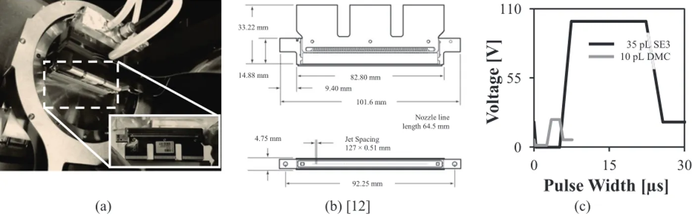
Material Printer 3000 (DMP 3000) from Fujifilm Dimatix. SE3 industrial print-heads from Fujifilm Dimatix were installed in DMP 3000 and were used for depositing the three basic layers which are conductive layer/electrodes, dielectric and conductive layer/electrodes. A typical architecture of a SE3 print-head can be seen in the Fig. 2 (a) and (b) below along with the waveform adapted for higher drop volume [12]. In Fig. 2 (c) the jetting waveform for 10 pL print-head is depicted with the thicker line and SE3 industrial print-head with the thicker line. SE3 print-heads can eject a nominal drop volume of 35 pL from a swath of 128 available nozzles for printing.
(a) (b) [12] (c)
FIGURE 2. (a) Photograph of SE3 industrial print-head with DMP 3000 jetting assembly containing SE3 print-head installed
within the system, (b) internal architectural dimensions of a SE3 industrial print-head, and (c) jetting waveform for SunTronic EMD 5603 silver ink for DMC 10 pL print-head (grey line) and SE3 industrial 35 pL print-head (black line)
TABLE 1. Deposition parameters for the different printing layers and for the various electronic devices (exemplary) Layer
Sequence Layer
Targeted inkjet-printed
device Ink Print-head Drop Space
Jetting frequency & Voltage
No. of nozzles 1. Bottom Gate/ Electrodes
capacitors, OTFTs, resistors SunTronic EMD 5603 silver ink SE3, 35 pL 40 μm 90-100 V 5 kHz, Approx. 70 2. Dielectric Middle capacitors, OTFTs dielectric cPVP
ink SE3, 35 pL 20- 50 μm, with 10 μm step 5 kHz, 75-80 V Approx. 70 3. or Top Contact Source/ Drain
Electrode capacitors, OTFTs SunTronic EMD 5603 silver ink SE3, 35 pL 35- 50 μm, with 5 μm step 5 kHz, 90-100 V Approx. 40 4. Semiconductor Organic OTFTs FS0087 DMC, 10 pL 20 μm 20-23 V 5 kHz, Approx. 10-12 With correspondence to the drop volume, the drop space (μm) or the resolution in dots per inch (dpi) the digital patterns were adapted and then designed. The patterns are adjusted such that around 400 to 600 individual kind of electronic devices or mixture of both are includes in one A4 sized sheet. The SunTronic EMD 5603 silver ink used for printing the Bottom Gate/ Electrodes and the Source/Drain or Top Electrodes was sintered in convection oven at 135 ºC for 30 min. On the other hand, cPVP dielectric ink layer was first let to dry at the fume cupboard for 30 mins and then thermally cured in the vacuum oven at at 120° C for 1 hr. The OTFTs discussed here are inter-digitated, this assures higher efficiency of the OTFTs. Preliminary tests are also included for determining the optimal drop
0 55 110 0 15 30
V
oltage
[V
]
Pulse Width [μs]
35 pL SE3 10 pL DMC 33.22 mm 14.88 mm 9.40 mm 82.80 mm 101.6 mm Nozzle line length 64.5 mm Jet Spacing 127 × 0.51 mm 4.75 mm 92.25 mmspace for printing Source/Drain electrodes. Exemplary, digital A4 sheets containing OTFTs with Channel Length/ Channel Width (W/L) ratio of 1000 is considered. Different drop spaces are varied for obtaining the variability in the performance of the OTFT device. Also the digital pattern for other devices such capacitors and resistors are adapted for printing on A4 sized foils. The active areas and layer thicknesses of the capacitors are varied and then the yield of the working devices was calculated. Similar kind of variability is also performed for the printing of OTFTs. The digital patterns are adjusted by incorporating the design compensation rules for the different dimensions, device structures, architecture and layout of the individual printing layers. Below in Fig. 3 (a) an example is shown where the printing workflow and the pattern compensations are defined. Here in Fig. 3 (b), compensation of the digital images is shown. This indicates the addition of some pixels at the beginning of the Source/Drain Electrode, which will compensate the intrinsic deficiency of the inkjet printer.
In contrast to the devices which are printed with the industrial equipment and print-heads, a logical inverter circuit is also fabricated using Dimatix Material Printer 2831 (DMP 2831) from Fujifilms Dimatix (laboratory desktop printer) and inexpensive DMC print-heads. In this case two OTFTs, one big with higher and the other one with lower W/L ratio is considered to be connected.
(a) (b)
FIGURE 3. (a) Schemes for printing OTFTs by using digital bitmaps arranged for A4 size deposition and architecture for OTFT,
and (b) Example of a single OTFT (Source/Drain electrode) digital bitmap which shows with and without implementing the compensation tools
Characterization Techniques: The mentioned devices are optically characterized by light microscopy using a
Leica DM 4000 M light microscope. The layer morphology and thickness is measured by mechanical surface profile-meter Dektak 150 from Vecco. Also, the devices are electrically characterized using a semi-automatic measurement probe station equipped with a voltage source meter and the data accumulation and storage is also done automatically using the compatible software routines. All the electrical measurements for the different kind of devices are done under standard atmospheric condition.
RESULTS & DISCUSSIONS
Below in Fig. 4 microscopic images of the drops, lines and solid rectangles are shown. These are the basics for printing several kinds of devices e.g. capacitors and OTFTs, using the mentioned SunTronic EMD 5603 silver ink and cPVP dielectric ink respectively. From the microscopic images in Fig. (a) and Fig. 4 (f), it was seen that the average diameter of a printed 1) silver drop on foil is 80 ± 5 μm, and 2) cPVP drop on foil is 85 ± 10 μm. Similarly, a printed silver line had an average line width of 100 ± 5 μm. The effects of evaporation on the wet printed layers for the two dissimilar inks (silver & cPVP) are different. From the microscopic images in Fig. 4 (f) and (g) it can be seen clearly that for printed cPVP drop and also solid areas, the cross-sectional thickness at the borders of the layer are much higher when compared to the silver layer. Below in Fig. 4 (d) & (h) shows the cross-sectional surface profiles of the two printed ink drops. The average drop thickness of silver and cPVP was found to be 280 ± 10 nm
1
2
3
4
4. Organic Semiconductor 3. Source/Drain or Top Contact Electrode
2. Middle Dielectric 1. Bottom or Gate Electrode
NO compensation in digital image
Compensation in digital image
and 370 ± 70 nm respectively. Similarly the coffee ring effect can also be seen in the printed layers. Below in Fig. 4 (e) and (i) are shown the sectional layer profiles for printed silver (drop space of 40 μm, average layer thickness of 0.65 ± 0.2 μm) and cPVP (drop space of 30 μm, average layer thickness of 0.93 ± 0.45 μm) layers. This high deviation in the thickness value for the printed cPVP layer is due to the peaks at the border. But at the active area, the measured layer thickness was found to be 1.5 ± 0.3 μm).
(a) (b) (c)
(d) (e)
(f) (g)
(h) (i)
FIGURE 4. Microscopic images of (a) drops, (b) lines, (c) solid area printed with SunTronic EMD 5603 silver ink on foil;
surface profile of (d) drop and (e) solid area printed from SunTronic EMD 5603 silver ink; microscopic images of (f) drops and
0 0.5 1 0.14 0.19 0.24
Measured
thickness
[μm]
Scanned length [mm]
0 6 12 0 0.75 1.5Measured
thickness
[μm]
Scanned length [mm]
0 0.5 1 0.05 0.15 0.25Measured
thickness
[μm]
Scanned length [mm]
0 6 12 0 1.5 3Measured
thickness
[μm]
Scanned length [mm]
Print Direction 500 μm 1 mm 200 μm 30 μm Drop space 400 μm 300 μm Drop space 40 μm 500 μm 1 mm Print Direction Drop space 50 μm 200 μm 30 μm Drop space 200 μm Drop space 30 μm Print Direction(g) a solid area printed with cPVP dielectric ink on foil; and surface profile of (d) drop and (e) solid area printed from cPVP dielectric ink
Below in Fig. 5 (a), (b) and (c) shows the microscopic images of all inkjet-printed devices e.g. resistor, capacitor and OTFT printed on flexible A4 sized foils, which are fabricated with the industrial printing equipments. Exemplary results are shown for the printed devices e.g. capacitors and OTFTs.
(a) (b) (c)
FIGURE 5. Photograph & microscopic images of different all inkjet-printed devices (a) resistors, (b) capacitors and (c) OTFTs
on A4 sized foil
Capacitors: Below in Fig. 6 are the graphs which show the electrical properties of the printed capacitors. The
indicated results are derived from 420 capacitors which are printed in 3 different sheets but with the same deposition process parameter. It can be seen from Fig. 6 (a) that there is no significant change in the normalized capacitance value when the active area of the capacitor is changed from 1 mm2 to 16 mm2 for drop space of 40 μm. The
deviation caused in the capacitance is much higher when the drop space is increased from 50 μm to 60 μm. The reason can be due to the varied layer thicknesses and also the varied morphology obtained due to the evaporation-induced material transport flows inside the deposited layer. Also it could be seen that for higher active areas, the number of failing devices increase and therefore the yield decreases. The best compromise achieved for getting the maximum stable capacitance is in the range of 1 mm2 to 9 mm2 when the variables like drop space, fabrication yield
and active areas is considered.
(a) (b)
FIGURE 6. Graph showing function of (a) normalized capacitance over varied active areas and drop spaces, and (b) yield
percentage over active area for the all inkjet-printed capacitors (for drop space 40 μm)
Organic thin film transistors: Below in Fig. 7, are shown the microscopic images for the all inkjet-printed
OTFTs (exemplary). In total 616 OTFTs were printed with stable deposition process parameters.The most critical deposition step for fabricating OTFTs was the printing of the Source/Drain electrodes. The drop space for printing the Source/Drain electrodes were varied between 35 μm to 50 μm (step of 5 μm drop space). Drop space of 50 μm gave rise to maximum number of open circuit defects, where the inter-digitated Source/Drain electrodes were not
0.0 0.1 10.0 1 4 9 16 25
C
apacitance
[nF
/cm
2]
Active area [mm
2]
40 um 50 um 60 um 0.0 50.0 100.0 1 4 9 16 25Yield
[%
]
Active area [mm2] 40 μm 500 μm 500 μm 500 μmconnected totally. And, at the lower drop spaces (35 μm and 40 μm) resulted into higher percentage of interruption between Source/Drain electrodes which gives rise to short circuits. As a result, the most appropriate drop space was found to be 45 μm.Below in Fig. 7. (a), (b) and (c), the real channel lengths achieved after the printing and post-treatment process are shown. It was found that for a digital channel length of 40 μm, 50 μm, and 70 μm; a real channel length of 25 ± 10 μm (mainly short circuits), 30 ± 5 μm (good OTFTs) and 50 ± 10 μm (operational OTFTs) respectively could be achieved. Therefore a digital channel length of 40 μm was selected which provided the least number of short circuits for a stable printing process condition.
(a) (b) (c)
FIGURE 7. Microscopic image of Source/Drain electrodes using digital channel lengths of (a) 40 μm, (b) 50 μm and (c) 70 μm
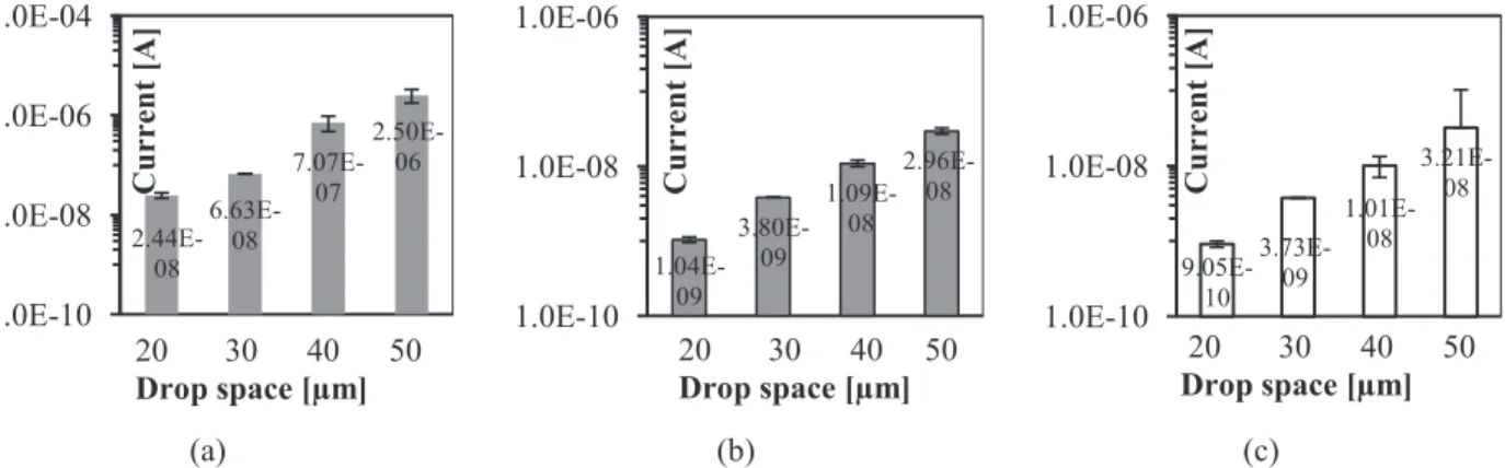
Figure 8. (a), (b) and (c) refer to the electrical performance exhibited by the OTFTs printed with similar deposition process condition and also same configuration (W/L = 1000). It can be seen that the current at Source/Drain (ON current) increases with the increasing drop space or lower layer thickness for the cPVP dielectric and so as the OFF current.
(a) (b) (c)
FIGURE 8. Graph showing the OTFT (W/L = 1000) performance as a function of cPVP dielectric layer thickness (varied drop
space) (a) Source/Drain current, (b) OFF current, (c) Gate/Source current through the cPVP dielectric layer
A maximum and a minimum Source/Drain current of 2.5 μA and 24.4 nA were obtained, when the layer thickness for the cPVP dielectric is the maximum and minimum respectively. This can be correlated inversely with the drop space of 50 μm and 35 μm. On the contrary, the leakage current through the Gate dielectric also increases with increase in the drop space. This is due to the instability arising from the dielectric when the layer thickness is
2.44E-08 6.63E-08 7.07E-07 2.50E-06 1.0E-10 1.0E-08 1.0E-06 1.0E-04 20 30 40 50 Drop space [μm] 1.04E-09 3.80E-09 1.09E-08 2.96E-08 1.0E-10 1.0E-08 1.0E-06 20 30 40 50 Drop space [μm] 9.05E-10 3.73E-09 1.01E-08 3.21E-08 1.0E-10 1.0E-08 1.0E-06 20 30 40 50 Drop space [μm] Current [A] Current [A] Current [A] 500 μm 500 μm 30 μm 30 μm 30 μm Short circuits between Source/Drain electrodes 500 μm
Increasing Channel Length for Source/Drain electrodes on dielectric
lowered. Therefore a compromised drop space of 40 μm is suitable for a reasonable electrical characteristic which will give the lowest leakage current. The highest ON/OFF ratios and the charge carrier mobility for the used organic semiconductor for the OTFTs were obtained at drop space 40 μm and 50 μm (drop space for cPVP dielectric). In total, it was found that yield of about 70 % could be achieved from the OTFT discussed here (similar and good working devices).
Also, an all inkjet-printed inverter was developed within the TDK4PE consortium (EU funded project). As mentioned earlier, the inverter performance shown below is fabricated from the laboratory desktop inkjet printer using inexpensive print-heads. The inconsistent stability in the printing process of the entire inverter circuit indicated low fabrication yield. The inverter showed an approximate gain of 2.5 and the performance of the inverter persistently degraded during the prolonged basing process. Hence this indicates the requirement towards a more stable fabrication process for the electronic devices suitable to fit into the criteria for building-up electronic logical circuits.
SUMMARY
As a summary it can be stated that inkjet technology has a massive potential towards printing of large area electronics on flexible substrates. Herein, the inkjet printing of electronic devices such as capacitors, resistors and OTFTs have been exhibited with the varying morphological and electrical characteristics. The fabrication yield of all inkjet-printed capacitors (printed with industrial print-heads and equipments) show an adverse trend towards the increasing deposited area and also the drop space. These adverse trends are seen because of the transfer of the cPVP (dielectric material) towards the edges during the drying process of the printed layer. The fabrication yield for the Source/Drain electrodes of the all inkjet-printed OTFTs (printed with industrial print-heads and equipments) show the direct correlation with the increasing drop space. As the drop space increases, the amount of defects caused due to the short circuit between the Source/Drain electrodes decreases. This yield mostly reflects the absolute fabrication yield for the printed OTFTs. The printed OTFTs performance is also exhibited with the varying drop space for the printed cPVP dielectric layer. The up-scaled inkjet deposition process for fabricating the electronic devices from print-heads delivering 10 pL to 35 pL drop volume, and from the used 16 to 128 nozzles give rise to different layer morphologies and hence also the devices characteristics. The routes to achieve higher fabrication yield for the all inkjet-printed electronic devices suitable for logical circuits on flexible substrates are the possible only with the industrial print-heads and equipments.
ACKNOWLEDGMENTS
This present work is a part of a European funded Project under the framework of FP7-ICT “Technology & Design Kit for Printed Electronics” TDK4PE (contract no. 287682). I like to acknowledge Prof. Henrique. L. Gomes and his research group (Universidade do Algarve, Institute of Telecommunications, Faro, Portugal) who have been also contributing for characterizing the printed devices within the TDK4PE consortium. I also would like to acknowledge Mr. Christoph Sternkiker and Mr. Sunil Kapadia working under the Professorship of Digital Printing and Imaging Technology for providing me the necessary support for this research work.
REFERENCES
1. Seungjun Chung et al., “All-Inkjet-Printed Organic Thin-Film Transistors with Silver Gate, Source/Drain Electrodes”, Jpn. J. Appl. Phys. 50, (2011)
2. Takeo Kawase et al., “Inkjet Printing of Polymeric Field-Effect Transistors and Its Applications”, Jpn. J Appl. Phys., Vol. 44, No. 6A, 3649-3658, (2005)
3. Seungjun Chung et al., “All-Inkjet-Printed Organic Thin-Film Transistor Inverter on Flexible Plastic Substrate”, IEEE electron device letters, Vol. 32, No. 8, 1134-1136, (2011)
4. Jin Jang et al., “High performance ink-jet printed diketopyrrolopyrrolebased copolymer thin-film transistors using a solution processed aluminium oxide dielectric on a flexible Substrate”, J. Mater. Chem. C, 1, (2013) 5. Jung-Pyo Hong et al., “Tuning of Ag work functions by self-assembled monolayers of aromatic thiols for an
efficient hole injection for solution processed triisopropylsilylethynyl pentacene organic thin film transistors”, Appl. Phys. Lett. 92, (2008)
6. Yi Liu et al., “An all-inkjet printed flexible capacitor on a textile using a new poly(4-vinylphenol) dielectric ink for wearable applications.” in Proc. Sensors IEEE, 1-4, (2012)
7. Y. Liu et al., “An all-inkjet printed flexible capacitor for wearable applications,” in Symposium on Design, Test, Integration and Packaging of MEMS/MOEMS, Cannes Côte d'Azur, France, 192-195, (2012)
8. B.J. Kang et al., “All-inkjet-printed electrical components and circuit fabrication on a plastic substrate”, Microelectronic Engineering, Vol. 97, No. 9, 251–254, (2012)
9. B.S. Cook et al., “Multi-Layer RF Capacitors on Flexible Substrates Utilizing Inkjet Printed Dielectric Polymers”, Microwave and Wireless Components Letters, vol. 23, no. 7, 353-355, (2013)
10. Kenjiro Fukuda et al., “Fully Solution-Processed Flexible Organic Thin Film Transistor Arrays with High Mobility and Exceptional Uniformity”, Scientific report in Nature, DOI: 10.1038/srep03947, (2014)
11. Robert Abbel et al., “Industrial-scale inkjet printed electronics manufacturing—production up-scaling from concept tools to a roll-to-roll pilot line”, Transl. Mater. Res., (2014)
12. SE3 printhead for DMP 3000, Fujifilm Dimatix,
URL: http://www.fujifilmusa.com/products/industrial_inkjet_printheads/print-products/printheads/materials-deposition/se3/index.html#features, last visited on 05.092014, 13:30 hrs