Brazilian Journal of Physics, vol. 29, no. 4, December, 1999 715
Quantum Hall Eect in a Wide
Parabolic Quantum Well
G.M.Gusev 1
, J.R.Leite 1
,E.B.Olshanetskii 2
,D.K. Maude 2
,
M. Casse 2;3
, J.C.Portal 2;3
, N.T. Moshegov 4
, and A.I.Torop ov 4
1Instituto de Fsica da Universidade de S~ao Paulo,
CP 66318, CEP 05315-970, S~ao Paulo, SP, Brazil 2CNRS-LCMI, F-38042, Grenoble, France 3INSA-Toulouse, 31077, France
4Institute of Semiconductor Physics, Novosibirsk, Russia
Received February 8, 1999
We investigate the activated conductivity for Landau levels at lling factors =1,2 in a parabolic Al
x Ga
1,xAs well down to 30 mK. We obtain a very small activation energy
0.02 meV, which is
almost 1-2 orders of magnitude smaller than the expected values for energy gaps in a wide quantum well. The resistivity minima vanish completely when a parallel component of magnetic eld is applied. The collapse of the energy gaps in the wide parabolic well occurs due to the new electron correlated state, probably the charge density wave state predicted for a uniform wide electron slab in high magnetic eld.
I Introduction
The Quantum Hall eect (QHE) is characterized by narrow resistivity peaks separated by deep minima [1]. These resistivity minima arise due to the localization of the electron states at the Fermi energy, when it lies in the gaps between Landau or spin split levels. In this regime the resistivity is determined by the elec-tron thermal activation with an energy gap h!c where
!c =eB/mc- cyclotron frequency for Landau levels and
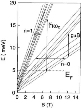
gB/2 for spin split levels. Here is the Bohr magne-ton, g is the eective Lande factor, which is strongly enhanced in a two-dimensional electron gas due to the electron-electron interactions. The temperature depen-dence of the resistivity minima can therefore be used to study energy gaps in the quantum Hall eect. Sev-eral experiments have been performed to study the ex-change enhanced Landau and spin splitting [2], com-posite Fermions cyclotron energy [3] and skyrmions [4]. In a conventional picture the quantum Hall eect is predicted to disappear for a suciently wide quantum well. Fig.1 shows the energy spectrum as a function of magnetic eld B for a wide square quantum well. At suciently high B the Fermi energy crosses the en-ergy levels corresponding to the lowest Landau level of each subband. Therefore, it is expected that for a wide quantum well the last resistivity minima could be due to the energy gap between electric subbands, and not to Landau levels. In a real system the
716 G.M.Gusevet al.
the curvature of the parabolic potential !0. For the
published magnetotransport experiments with sample parameters h!0 =2.9 meV the critical thickness was
found to be dc=1000 A. However, the destruction of
the =1 plateau has not been observed in experiments in wide well structures with thickness1500 A [6]. We
perform our experiments with thicker electron slab.
Figure 1. Energy diagram for a wide square well. The cy-clotron, Zeeman and subband energies are indicated.
II Experimental results and
discussion
The samples used are the GaAs-AlxGa1,xAs parabolic
quantum well grown by molecular-beam epitaxy. On the top of the semi-insulating substrate there is a 1000 nm GaAs buer layer with 20 periods of a AlAs(5ML)GaAs(10ML) superlattice, followed by 500 nm GaAs-AlxGa1,xAs with x varying from 0.07
to 0.27, 100 nm Al0:3Ga0:7As with -Si doping,
Al0:3Ga0:7As undoped layer (spacer), the 200 nm -wide
parabolic well with the alloy composition x in the range 0 < x < 0:19. Two structures have been studied, A and B, the main dierence between these is that the parabolic well A has a spacer with smaller thickness 100 A in comparison with 400 A for sample B. It leads to the dierence in the electron density: sample A has
concentration ns in the dark 3.9 10
11cm,2, sample B
- 0.5410
11cm,2. After growth the substrate with the
parabolic quantum well (PQW) was processed into Hall bars. Four-terminal resistance and Hall measurements were made down to 30 mK in magnetic elds up to 17 T. The distance between the voltage probes was 250 m and the width of the bar was 100 m. The measure-ments were performed with an ac current not exceeding 10,8 A. The resistance was measured for dierent
an-gles between the eld and thesubstrate plane in mag-netic eld using an in situ rotation of the sample. The three dimensional pseudocharge is n3D=2/(e
2W2),
where W is the well width, =12.5 -dielectric constant for GaAs =150 meV- height of the parabola. We nd n3D=2.1
10
16cm,3which corresponds to the classical
width of the 3D electron gas for the sample A we =
ns/n3D=190 nm and we= 26 nm for sample B.
There-fore we can compare the behaviour of the QHE for the narrow and for the wide electron layers. For the wide parabolic well the sample layer is close to the geometri-cal width of the well, therefore the energy spectrum Ei
of a parabolic well can be roughly approximated by the spectrum of a square well Ei =i
2(h/w e)
2/8m
e , where
me is a eective electron mass. The mobility of the
electron gas in the well is 27010
3cm2/Vs for sample
B and 6510
3cm2/Vs for sample A.
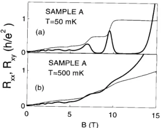
The magnetoresistance and Hall eect data for sam-ple A at dierent temperatures are shown in Fig.2. We see that in strong magnetic elds and low tempera-tures the sample reveals the usual Quantum Hall ef-fect. However, the resistance peaks at lling factors n=3/2 and 5/2 are completely smeared out at 0.5 K. For the parabolic well with smaller layer width (sample B) the QHE is still clearly seen at T=0.9 K. Fig. 3 shows the temperature dependence of the diagonal re-sistivity from 30 to 900 mK for sample A. The inset in Fig. 3a shows activated resistivity at =1 (circles) and 2 (squares) minima which can t to an Arrhenius plot. Saturated behaviour is found at T< 50 mK, which could be due to sample heating. The energy gaps calculated from the Arrhenius plot are very small 0.02 meV.
Brazilian Journal of Physics, vol. 29, no. 4, December, 1999 717 B=5 T (Fig.2 a) and the neighboring minima are also
completely smeared out at T=0.5 K. We should note that for the sample B the energy gaps calculated from the Arrhenius plot for minima 1 and 2 are coincident with the gaps which are expected for Landau and spin splitting.
Figure 2. Longitudinal and Hall resistivities for a wide parabolic well at T=50 mk (a) and T=500 mK (b).
Numerical calculations for a square well of width we=190 nm yield the following energies for the rst
5 electric subbands : E1=0.19 meV, E2=0.75 meV,
E3=1.7 meV, E4=3 meV, E5=4.7 meV. We determine
the electron density for the dierent occupied electric subbands from the Fourier power spectrum of the Shub-nikov de Haas oscillations at low magnetic elds. We obtain densities 1.410
11cm,2 , 0.9 10
11cm,2and
0.5510
11cm,2. We should note that probably we are
not able to separate oscillations corresponding to the 1/B frequencies from the rst and second subbands. In this case it is reasonable to estimate the electron den-sity for the second subband as 1.3-1.210
11cm,2. The
upper subband has lower electron density and we are not able to detect it. The total density Ns= 4.05-4.15
1011cm,2is in good agreement with the QHE high eld
data ( Ns= 3.9 10
11cm,2) . The energy separations
between subbands ( E21
0.5 meV, E
31=1.8 meV,
(E41=3 meV) also are in good agreement with
the-oretical values for the square well (E21 = 0.56 meV,
E31=1.5 meV, E41=2.8 meV). In a parallel
mag-netic eld we observe 4 peaks in the magnetoresistance curve due to the magnetic depopulation of levels, which is also in accordance with our calculations. Within a single electron model, application of a magnetic eld perpendicular to the plane of the quantum well forms a fan of Landau levels originating from the energy levels of each electric subband. Fig. 1 illustrates the mag-netic eld dependence of the energy levels of a square
well with thickness 186 nm including Zeeman splitting. One can see here that at magnetic eld B>5 T the Zee-man energy is larger than the separation between the second and third electric subbands in accordance with calculations of spin eects in a wide parabolic quan-tum well [8]. Thus, minima at =1, 2 correspond to the Fermi energy lying in the energy gap E21 and
E31. In strong magnetic elds only the last Landau
level of the lower electric subband is occupied, thus the last minimum should be observed at B=16 T. Fig. 2 shows that at B>13 T the diagonal resistance starts to grow, however the well developed Hall plateau are still seen at higher magnetic elds. This behaviour cor-responds to the metal-Hall insulator transition, which has been observed previously in narrow GaAsAlGaAs and InAs/GaAlInAs quantum wells [9]. Therefore for the last minimum in the diagonal resistance, the Fermi level does not lie in the center of the E21 gap. This
shift of the metal Hall insulator transition to the lower eld could be due to the smallness of the E21energy
gap. Also, as we mentioned above, Hartree Fock cal-culations suggest a new charge density wave state or a Wigner crystal [9] at strong magnetic elds. The min-imum destruction and resistance growth could be due to the pinning of this sate by impurities.
718 G.M.Gusevet al.
III Conclusion
In summary, we measured the Quantum Hall eect in a wide quantum well and found very small activation in the resistivity minima energy at lling factors 1 and 2. Existing theory predicted such suppression in the =1
quantum limit due to the formation of a charge density wave. Small activation energies at=1,3 have been
ob-served in a double quantum well [10], which also has been explained by phase transition to a charge density wave state [11]. We should note that the calculations also have been done only in the strong magnetic eld corresponding to=1.
Acknowledgements
This work was supported by CNPq , FAPESP and COFECUB/USP. GMG is supported by CNPq, EBO acknowledges grant from Ministere de l'Education Na-tionale de la Technologie, France.
References
[1] see for review, R.E. Prange, S.M.Girvin eds., The Quantum Hall eect, second edition (Springer-Verlag,
New York, 1990).
[2] A. Usher, R.J. Nicholas, J.J. Harris, C.T. Foxon, Phys. Rev.B,41, 1129 (1990).
[3] R.R. Du, H.L. Stormer, D.C. Tsui, L.N. Pfeier and K.W. West, Phys. Rev. Lett.,70, 2944 (1993).
[4] A. Smeller, J.P. Eisenstein, L.N. Pfeier, K.W.West, Phys. Rev.Lett., 75, 4290 (1995), D.K.Maude,
M.Potemski, J.C.Portal, M.Henini, L.Eaves, G.Hill, M.A.Pate, Phys. Rev.Lett.,77, 4604 (1996).
[5] V. Celli, N.D. Mermin, Phys. Rev.140, A839 (1965).
[6] M. Shayegan, T. Sojoto, M. Santos, C.Silvestre , Appl. Physics Letters,53, 791 (1988).
[7] L. Brey, Phys. Rev. B,44, 3772 ( 1991).
[8] C.E. Hembree, B.A. Mason, J.T. Kwiatkowski, J. Furneaux, J.A. Slinkman, Phys. Rev. B, 48, 9162
(1993).
[9] D. Shahar, D.C. Tsui, M. Shayegan, R.N. Bhatt, J.E. Cunningham, Phys. Rev. Lett., 74, 4511 (1995), W.
Pan, D. Shahar, D.C. Tsui, H.P. Wei, M. Razeghi, Phys. Rev. B,5555, 15431 (1997).
[10] G.S. Boebinger, H.W. Jiang, L.N. Pfeier and K.W. West, Phys. Rev. Lett.,64, 1793 (1990).