Study of the Electrostatic Shielding and Environmental Interactions in Carbon Nanotubes by Resonance Raman Spectroscopy
Paulo Antˆonio Trindade Ara´ujo
Study of the Electrostatic Shielding and Environmental
Interactions in Carbon Nanotubes by Resonance Raman
Spectroscopy
Paulo Antˆonio Trindade Ara´ujo
Orientador: Prof. Ado J´orio de Vasconcelos
Tese de doutorado apresentada ao Departamento de F´ısica da Universidade Federal de Minas Gerais como requisito parcial para a obten¸c˜ao do grau de Doutor em F´ısica.
Acknowledgments
• Agrade¸co ao meu orientador Prof. Dr. Ado J´orio de Vasconcelos pelo apoio, pelas oportunidades concedidas e, principalmente, pela amizade.
• Agrade¸co ao Prof. Dr. Luiz Gustavo Can¸cado pelas valiosas discuss˜oes t´ecnicas e te´oricas sobre o campo pr´oximo (N ear−f ield) e suas aplica¸c˜oes. Agrade¸co tamb´em por, juntamente com a L´u e o Linus, ter me recebido maravilhosamente bem em Rochester.
• Agrade¸co ao Prof. Dr Marcos Assun¸c˜ao Pimenta, pelo apoio e gentileza, deixando as portas do Raman sempre abertas pra mim.
• Agrade¸co aos meus pais e irm˜as pelo amor e compreens˜ao.
• Agrade¸co a Sandra Donato por me mostrar que o auto-conhecimento ´e, definitiva-mente, essencial para se viver bem.
• Agrade¸co a Ma´ıra e ao Luca, meu filhinho lindo. Os dois representam muito para mim.
• Agrade¸co aos meus queridos amigos, Mario, Dandan, Xubaca, Newton, Leonardo, Marcelo, Patrick e Dani pelo apoio e compreens˜ao.
• Agrade¸co aos amigos do departamento de f´ısica pela ´otima convivˆencia.
• Agrade¸co `a todos os meus colaboradores que, logicamente, foram fundamentais. ´E uma honra trabalhar com vocˆes.
• Ich moechte Prof. Achim Hartschuh danken. Er hat mir die Grundregel von NahFeld gelehrt. Vielen danke!
3
• I would like to thank the Profs. Mildred Dresselhaus and Richiiro Saito for sharing with me an unmeasurable professional experience, allowing me to realize what real science is about.
• Agrade¸co a Marluce e a Ieda por toda ajuda e galhos quebrados. • Agrade¸co a nossa querida Idalina. Que ela esteja descan¸cando em paz.
Contents
RESUMO iv
ABSTRACT v
1 Introduction 1
I
Theoretical Background
4
2 Carbon Nanotubes and Raman Scattering: Basic Concepts 6
2.1 What is a SWNT? . . . 6
2.1.1 The electronic structure . . . 8
2.1.2 The vibrational structure . . . 17
2.2 Resonance Raman spectroscopy and SWNT characterization . . . 23
2.2.1 A guide to the Raman-based (n, m) assignment . . . 26
2.3 Summary . . . 30
3 The Historical Overview of Eii: van Hove singularities, Excitons and the Screening Problem 33 3.1 The evolution of the experimental determination of Eii . . . 33
3.2 The dielectric screening effect . . . 38
3.3 Summary . . . 41
II
Instrumentation Development and Results
42
4 Instrumentation Development: Going Beyond the Micrometer Scale 44 4.1 Nano-spectroscopy and manipulation - I . . . 444.1.2 The Angular Spectrum Representation . . . 50
4.1.3 Confocal microscopy: the experimental setup . . . 52
4.1.4 The detection systems . . . 56
4.2 Nano-spectroscopy and manipulation - II . . . 61
4.2.1 The scanning probe microscope control - RHK . . . 61
4.2.2 The scan-head configuration . . . 69
4.2.3 The Shear-force mechanism . . . 87
4.2.4 The Easy-PLL plus . . . 95
4.2.5 Going beyond the classical optical limits: near-field optics . . . 98
4.2.6 Converting Gaussian polarized beams into radially polarized beams 102 4.2.7 Shielding the system against noises . . . 104
4.3 Results: Testing the system . . . 105
4.3.1 Confocal microscopy measurements . . . 105
4.3.2 Atomic force microscopy (AFM) measurements . . . 106
4.3.3 Near-field measurements . . . 110
4.4 Summary . . . 114
5 Environmental Effects on the SWNTs Radial Breathing Mode Frequency ωRBM 115 5.1 The ωRBM vs. dt relation and the role of a changing environment . . . 115
5.2 The effect of the environment on the ωS.G. RBM . . . 120
5.3 Summary . . . 124
6 Environmental and Screening Effects on the SWNTs Energy Transitions Eii 125 6.1 The effect of dielectric screening on Eii . . . 125
6.1.1 The EM 11 and E22M transitions . . . 128
6.1.2 The ES.G. ii exhibits the highest Eii values . . . 130
6.2 The dt dependence of the dielectric constant for the excitonic Eii . . . 133
6.3 The θ dependence of the dielectric constant for the excitonic Eii . . . 138
6.4 Unifying the Eii’s κ dependence: the importance of the exciton’s size . . . 141
6.5 Summary . . . 144
7.2 Pressure-modulated G-band Raman frequencies in carbon nanotubes . . . 153 7.3 Summary . . . 155
8 Conclusions 157
A Raman Spectroscopy: Experimental Details 160
A.1 The micro-Raman spectrometers . . . 160 A.2 The excitation sources . . . 161
Resumo
Na ´ultima d´ecada, muitos avan¸cos experimentais e te´oricos foram feitos na fotof´ısica dos
nanotubos de carbono de parede ´unica (SWNT). Tais conquistas nos permitiram alcan¸car um profundo conhecimento da f´ısica por tr´as da dependˆencia com os ´ındices (n, m) das energias de transi¸c˜ao ´opticas (Eii) e da frequˆencia do modo de respira¸c˜ao (ωRBM). A primeira parte deste
trabalho discute a pesquisa que tenho feito, baseado na espectroscopia Raman ressonante do
modo radial de respira¸c˜ao, sobre as propriedades eletrˆonicas e vibracionais dos SWNTs. Estas
pesquisas foi direcionada para o entendimento de como uma mudan¸ca no ambiente em torno
dos SWNTs muda a rela¸c˜ao existente entre (Eii, ωRBM) e (n, m). Ser´a mostrado que mudan¸cas
ambientais fazem com que as frequˆencias do modo radial de respira¸c˜ao aumentem. Isto acontece
porque as paredes dos SWNTs interagem com o ambiente em torno dela atrav´es de for¸cas de Van
der Waals, que adicionam uma constante de mola extra, em paralelo ao sistema dos SWNTs.
As mudan¸cas nas Eii s˜ao explicadas em termos das mudan¸cas na constante diel´etrica κ, que
´e formada por duas comtribui¸c˜oes: a constante diel´etrica κtube, que depende das propriedades
intr´ınsecas de cada SWNT e a constante diel´etricaκenv, que depende somente do ambiente. Hoje
em dia, a comunidade cient´ıfica enfrenta o desafio de fazer experimentos na escala nanom´etrica.
Portanto, a constru¸c˜ao de sistemas para experimentos de nano-manipula¸c˜ao (por exemplo,
con-stru¸c˜ao de nano-devices e litografia em escala nanom´etrica) e nano-caracteriza¸c˜ao (por exemplo,
caracteriza¸c˜ao ´otica e medidas de transporte) tornou-se uma necessidade. Na segunda parte
deste trabalho, um sistema de microscopia confocal foi unido a um sistema de microscopia de
for¸ca atˆomica (AFM). Com o sistema confocal, somos capazes de fazer espectroscopia com
res-olu¸c˜oes ´oticas pr´oximas de λ/2, onde λ ´e o comprimento de onda da excita¸c˜ao. O sistema de AFM nos permite fazer imagens e manipular sistemas na escala nanom´etrica. Os dois juntos nos permite a realiza¸c˜ao simultˆanea de experimentos de espectroscopia e nano-manipula¸c˜ao. Se
a ponta para o AFM for met´alica, ´e poss´ıvel realizar experimentos ´oticos com resolu¸c˜oes
deter-minadas apenas pelo diˆametro das pontas, indo al´em dos limites de difra¸c˜ao. Este sistema foi
utilizado para entender mudan¸cas nas estruturas eletrˆonicas e de fˆonons dos SWNTs quando
estes s˜ao precionados por uma ponta de ouro e, al´em disto, entender as influˆencias de segmentos
Abstract
In the last decade, many theoretical and experimental achievements have been made in
the photophysics of single wall carbon nanotubes (SWNTs). Such accomplishments allowed us to gain a deep understanding of the physics behind the otical transition energy (Eii) and the
radial breathing mode frequency (ωRBM) dependence on nanotube chiral indices (n, m). The
first part of this work is devoted to assemble and discuss what I have done on the research of
the SWNT electronic and vibrational properties, based on the radial breathing mode (RBM)
measured by resonance Raman spectroscopy. Attention is directed to the understanding of how
a change in the environment changes the correlation between (Eii, ωRBM) and (n, m). It will be
shown that the changes on the ωRBM due to a changing environment makes the frequency to
increase. This happens because the SWNT’s wall interacts with the environment through Van
der Waals interactions, which add an extra spring constant in parallel to the SWNT system.
The changes in Eii are explained in terms of changes in the dielectric constant κ which, in our
model, comprises both, the dielectric constantκtube, that is intrinsically dependent of the SWNT
structure, and the dielectric constant κenv, that depends on the environment. Nowadays, the
scientific community faces at the challenge of performing experiments in the nanometer scale.
Therefore, to build systems for nano-manipulation (i.e. nanoscaled device’s construction and
nanoscaled lithography) and nano-characterization (i.e. optical characterization and transport
measurements) experiments has become a major need. In the second part of this work, a
confocal microscopy setup was joined to an atomic force microscopy (AFM) setup. With the
confocal system, we are able to perform spectroscopy with optical resolutions coming close to
λ/2, whereλis the light source wavelength. The AFM system allows us to image and manipulate scaled systems. Together They allow simultaneous experiments of spectroscopy and nano-manipulation. If the AFM tip is metallic, it is possible to perform optical experiments with
resolutions delimited only by the tip diameter, going beyond the diffraction limits. Such a
system has been utilized to understand the changes on the electronic and vibrational structures
of SWNTs due to pressures imposed by a gold tip, and, besides this, to understand the influences
Chapter 1
Introduction
Due to their one-dimensional character, single-walled carbon nanotubes (SWNTs) exhibit unique electronic and vibrational properties that make them an interesting mate-rial for technological applications in electronics and optoelectronics [1, 2, 3, 4, 5, 6, 7, 8, 9]. Associated with each individual SWNT is a unique pair of indices (n, m) that fingerprints all of its properties [10]. Therefore, the knowledge of (n, m) is of great importance for defining the properties and applications for each SWNT [9, 10]. Quantum confinement is responsible for the rise of van Hove singularities in the SWNTs electronic and vibrational density of states, resulting in (n, m)-dependent optical properties [9, 10]. The most fre-quently used optically-based experimental technique to properly assign the (n, m) indices is resonance Raman spectroscopy (RRS). By knowing (1) the SWNT optical transition energy (Eii) and (2) the radial breathing mode frequency (ωRBM) as measured by RRS,
together with their (Eii, ωRBM) changes with a changing environment it is possible to
uniquely assign the (n, m) for an individual SWNT [11].
The last decade has been marked by an impressive development in understanding the nature of Eii in quasi one-dimensional SWNTs, where i = 1,2,3, ... denotes the
inter-subband transitions between theith valence and theith conduction band for a given
SWNT [11]. While the interest in the excitonic nature of Eii and the dielectric screening
in one-dimensional structures dates back to research in π-conjugated polymers [10], in carbon nanotubes the interest to these topics started in 2003 with the identification of the so-called “ratio problem” [12]. In 2007, Araujo et al. [13] and Michel et al. [14] showed that the scaling law for the exciton energies explaining the “ratio problem” breaks down for transitions with energies greater than EM
11. The superscripts S and M of E S,M ii
quantum-chemistry calculations and solid-state physics (tight-bind and first-principles) calculations give contradictory pictures [13, 15] due to a lack of knowledge about the dielectric screening in SWNTs. A large amount of information about the Eii transitions
is now available for a large range of tube diameters (0.7 < dt < 6 nm) [11], and the Eii
for SWNTs are now understood theoretically in terms of the bright exciton energy [10, 15, 16]. The Eii can now be accurately described by tight-binding calculations, including
corrections for curvature optimization and many-body effects [11], plus an empirically-based diameter and exciton size dependence for the dielectric screening in SWNTs [17, 18]. Parallel to the progress on understanding the Eii in greater detail, was the
devel-opment of the physics behind the radial breathing mode (RBM) frequency (ωRBM). The
RBM provides the spectroscopic signature of SWNTs [9, 10, 19], and the ωRBM depends
on the SWNT diameter (dt), which is related to the SWNT (n, m) structural indices by
dt= 0.142
√
3(n2+mn+m2)/π[19]. The experimental results in the literature have been
fitted with the relation ωRBM=A/dt+B, with values for A and B varying from paper to
paper [11]. The empirical constant factor B prevents the expected limit of a graphene sheet from being achieved, where theωRBM should go to zero whendt approaches infinity.
Therefore,B is supposedly associated with an environmental effect onωRBM, rather than
an intrinsic property of SWNTs. An environmental effect here implies the effect of the surrounding medium, such as bundling, molecules adsorbed from the air, surfactant used for SWNT bundles dispersion, or substrates on which the tubes are sitting. Nowadays, the relation between ωRBM and dt is described by ωRBM = (227/dt)
√
1 +Ce·d2t, where
Ce is the only adjustable constant that weights the effect of the medium surrounding the
SWNTs [11].
wavelength. The AFM system allows us to image and manipulate nano-scaled systems. Together They allow simultaneous experiments of spectroscopy and nano-manipulation. If the tip used is metallic, the system also allows “Tip Enhanced Spectroscopy” (TES) to be done. As a consequence, optical resolutions beyond the diffraction limit can be achieved, where the resolution is totaly related to the diameter of the tip. This makes the equipment ideal to study, for example, the specific changes in the SWNTs properties caused by structural defects and local dopants [20]. Such a system has been utilized, in this work, to understand the changes on the electronic and vibrational structures of SWNTs due to pressures imposed by a gold tip, and, besides this, to understand the influences of segments of DNA in the photoluminescence signal of SWNTs@DNA systems.
This thesis is arranged as follows: In Chapter 2, a brief discussion about the SWNTs electronic and vibrational properties and resonant Raman spectroscopy is presented. In the last section of Chapter 2, a recipe for the SWNT (n, m) assignment is given. Chap-ter 3 gives an overview of the influences of the shielding caused by the environment on the excitonic transitions. Chapter 4 explains, in details, the nano-spectroscopy an manipula-tion experimental apparatus as well as the major needs to build one of it. In Chapters 5 and 6 the experimental achievements to understand how the ωRBM and the Eii change
Part I
Figure 1.1: Albert Einstein’s cartoon1.
“I’m not an atheist and I don’t think I can call myself a pantheist. We are in the position of a little child entering a huge library filled with books in many different languages. The child knows someone must have written those books. It does not know how. The child dimly suspects a mysterious order in the arrangement of the books but doesn’t know what it is. That, it seems to me, is the attitude of even the most intelligent human being toward God.”
Albert Einstein in a interview to the Time magazine.
Chapter 2
Carbon Nanotubes and Raman
Scattering: Basic Concepts
This chapter brings an overview of the electronic and vibrational structures of single wall carbon nanotubes (SWNTs) highlighting the main consequences of their circumfer-ential confinement, in special, the rise of the van Hove singularities. A special focus will be given to the radial breathing mode (RBM), which gives the main SWNT spectroscopic signature, and its dependence with the tube diameter (dt). A brief introduction to the
Raman scattering theory will be addressed. In the last section, a recipe to use the Raman scattering spectroscopy to perform the SWNTs (n, m) indices will be given.
2.1
What is a SWNT?
A single-walled carbon nanotube (SWNT) can be described as a single graphene sheet rolled up in a cylinder form, one atom thick [10, 19]. Each SWNT can be associated with a unique chiral vector, C⃗h:
⃗
Ch =n ⃗a1+m ⃗a2, (2.1)
which gives us the direction the graphene sheet is rolled up. As figure 2.1 shows, the C⃗h
is obtained by a linear combination of n times a⃗1 and m times a⃗2, where a⃗1 and a⃗2 are
the unit vectors used to describe the honeycomb lattice of the graphene.
The angle that C⃗h makes with relation to the unit vector a⃗1 (see the Fig. 2.1)
defines the called chiral angle (θ), which can vary fromθ= 0◦ (zigzag SWNTs) toθ = 30◦
Figure 2.1: The dashed rectangle represents the unit cell of a carbon nanotube (6,5). Two vectors are necessary to describe this unit cell and, therefore, the carbon nanotube structure: the chiral vector C⃗h and the translation vector T⃗, both of them described in
terms of a⃗1 and a⃗2 that are the unit vectors used to describe the honeycomb lattice of the
graphene. [21]
(|C⃗h|) also gives the SWNT diameter, dt:
dt= |
⃗ Ch|
π =
ac−c
√ 3 π (m
2+n2+mn)1/2, (2.2)
where ac−c is the nearest-neighbor Carbon-Carbon distance (1.421 ˚A in graphite). The
chiral angle is obtained by:
tanθ = |a⃗1×C⃗h| |a⃗1·C⃗h|
= √
3m
m+ 2n ⇒ θ = tan
−1[√3m/(m+ 2n)]. (2.3)
The indices (n, m) or the two parameters (dt, θ) completely determine a specific
SWNT and, therefore, its electronic and vibrational properties [9, 10, 19]. Besides the ⃗
Ch, the translation vector is also important to describe the SWNT’s unit cell. It gives the
periodicity of the unit cell along the SWNT axis and is defined by:
⃗
T =t1a⃗1+t2a⃗2 ≡(t1, t2), (2.4)
where the coefficient t1 and t2 are given by,
t1 =
(2n+m)
d and t2 =
−(2n+m)
The denominator dR is the greatest common divisor of (2n+m, 2m+n) and is equals
to d, if n−m is not a multiple of 3d, and 3d if n−m is a multiple of 3d. Here, d is the greatest common divisor of (n, m).
The unit cell of the SWNT is defined as the area delineated by the vectors T⃗ and ⃗
Ch. Since the real-space unit cell is much larger than that for a 2D graphene sheet, the 1D
Brillouin zone (BZ) for the nanotube is much smaller than the BZ for a graphene 2D unit cell. Because the local crystal structure of the nanotube is so close to that of a graphene sheet, and because the Brillouin zone is small, Brillouin zone-folding techniques have been commonly used to obtain approximate electron E(⃗k) and phonon E(⃗q) dispersion relations for carbon nanotubes with specific (n, m) geometrical structures. The vectors to describe the SWNT BZ are obtained with the relation,
⃗
Ri·K⃗j = 2πδij. (2.6)
It follows that: C⃗h·K⃗1 = 2π, T⃗·K⃗1 = 0, C⃗h·K⃗2 = 0 eT⃗ ·K⃗2 = 2π. The vectors K⃗1 and
⃗
K2 are related to the vectors b1 and b2 of the graphene’s BZ by,
⃗ K1 =
1
N(−t2b⃗1+t2b⃗2) (2.7) and
⃗ K2 =
1
N(m⃗b1−n⃗b2). (2.8)
The N wave vectors µ ⃗K1 (µ= 1-N/2, . . . ,N/2) give rise to N discrete⃗k vectors
or cutting lines in the circumferential direction (see Fig. 2.2). Here, N means the number of hexagons comprised by the SWNT unit cell. For each of the µ discrete values of the circumferential wave vectors, 1D electronic energy bands appears (oneπ-band and oneπ∗
-band), whereas eachµgives rise to 6 branches in the phonon dispersion relations. Because of the translational symmetry of T⃗, we have continuous wave vectors in the direction of
⃗
K2 for a carbon nanotube of infinite length. However, for a nanotube of finite length
(Lt) , the spacing between wave vectors is 2π/Lt , and effects on the electronic structure
associated with the finite nanotube length have been observed experimentally [9].
2.1.1
The electronic structure
Figure 2.2: (a) The graphene unit cell (dotted rhombus), containing sites A and B where carbon atoms are located, and (b) the graphene first Brillouin zone (shaded hexagon). a⃗i
and ⃗bi (i = 1, 2) are basis vectors and reciprocal lattice vectors, respectively. The high
symmetry points, Γ, K and M are indicated. (c) Parallel equidistant lines represent the cutting lines for the (4, 2) nanotube. The cutting lines are labeled by the cutting line index µ, which assumes integer values from 1 - N/2=-13 to N/2 = 14, where N is the number of hexagons inside the SWNT unit shell [9].
of solving the equation,
Ej(⃗k) = ⟨
ψj|H|ψj⟩
⟨ψj|ψj⟩
, (2.9)
where ψi and ψj are the Bloch’s functions given by:
ψ⃗k(⃗r) = ∑
j
cj(⃗k)φ⃗kj(⃗r), (2.10)
where φ⃗kj(⃗r) is given by:
φ⃗kj(⃗r) = √1 M
∑
l
ei⃗k. ⃗R(⃗l)ϕ
j(R⃗(⃗l)−⃗r). (2.11)
M is the number of unit cells,R⃗(l) is the vector giving the position of an atom in thel−th unit cell and ϕj is the j −th atomic orbital of the atom. It follows that the electronic
dispersion of the graphene is given by,
Eg2D(⃗k) =
ϵ2p±γ0ω(⃗k)
1±sω(⃗k) , (2.12)
where the function ω(⃗k) is given by,
ω(⃗k) =
√
|f(⃗k)|2 =
√
1 + 4 cos √
3kxa
2 cos kya
2 + 4 cos
2 kya
Figure 2.3: The graphene’s π and π∗ electronic dispersion calculated over the first BZ.
The inset shows the dispersion along the high-symmetry points. The values used for γ0
and s are, respectively, 3.033 eV and 0.129. [19]
The Eq. 2.12 is plotted as a function of⃗k, as exhibited in the figure 2.3.
However, in the case of SWNTs, the quantum confinement of the 1D electronic states must be taken into account [9]. The electronic σ bands are responsible for the strong in-plane covalent bonds within the 2D graphene sheets, while the π bands are responsible for weak van der Waals interactions between such graphene sheets in 3D graphite. The π bands are close to the Fermi level and then electrons can be optically excited from the valence to the conduction band. While in a graphene sheet we have a quasi-continuum of possibilities to choose wavevectors in the 2D reciprocal space, for SWNTs we have to consider the boundary conditions in the circumferential direction which limit us to certain wavevectors in the radial direction, giving rise to the cutting lines (see figure 2.2) [9, 19]. Then, by “cutting” the 2D graphene electronic dispersion with those allowed radial wavevectors, we obtain the SWNTs electronic dispersion as showed in the Fig. 2.4. Observe that, in the case of SWNTs, the conditione⃗k·C⃗h = 1 must be fulfilled. Therefore, k(πdt)=µ2π and then |K⃗1|=2/dt. It is worth to comment that N ⃗K1=−t2⃗b1 +t1⃗b2 is a
vector of the graphene’s reciprocal lattice. Sincet1 and t2 do not have common multiples,
it follows that µ=0, 1,...,N −1 or, equivalently, µ=1-N/2,...,N/2. Then, the electronic dispersion for SWNTs will be given by:
Eµ(⃗k) = Eg2D
[
k K⃗2 |K⃗2|
+µ ⃗K1
]
, (2.14)
Figure 2.4: (a) The calculated energy contours for the conduction and valence bands of a 2D graphene layer in the first Brillouin zone using the π-band nearest neighbor tight binding model [19]. The valence and conduction bands touch each other at the high symmetry K points. Thick solid curves show the cutting lines for the (4,2) nanotube, but translated to the first Brillouin zone of the graphene, the dark points indicating the connection between cutting lines. (b) Electronic energy band diagram for the (4,2) nanotube obtained by zone-folding from (a). (c) Density of electronic states for the band diagram shown in (b). [9]
transversal sections of the graphene’s electronic dispersion and the cuts are done every time the wavevectors obey the condition:
⃗k=k K⃗2 |K⃗2|
+µ ⃗K1, (2.15)
otherwise [9, 10]. The condition to have a metallic SWNT is that [(2n+m)mod3]=0. If [(2n+m)mod3]=1, the SWNT will be semiconducting type I. If [(2n+m)mod3]=2, the SWNT will be semiconducting type II.
Figure 2.5: Different types of SWNT: A SWNT is metallic ([(2n+m)mod3]=0) every time a cutting line touches the K point in the brillouin zone and it is a semiconducting otherwise ([(2n+m)mod3]=1(2)) [9, 10].
The optical transitions will occur around the high symmetry K points, where the expression forEii can, by approximation, be given as,
Eii(dt)≈2aC−Cγ0
p dt
, (2.16)
where p = 1,2,3,4, ... for ES
11, E22S, E11M, E33S.... Because of the trigonal warping effect
[9, 19],Eiialso presents a chiral angle dependence, which can be described byβpcos 3θ/dt.
The Eq. 2.16 becomes:
Eii(dt, θ)≈2aC−Cγ0
p dt
+ βpcos 3θ d2
t
, (2.17)
where βp is a parameter which must be adjusted to eachEii.
The σ−π orbitals mixing
The first-neighbor tight-binding model, together with the zone-folding method, are good enough to describe most of properties for carbon nanotubes with large diameters (dt > 1.2 nm). However, for small diameters (dt < 1.2 nm) it is necessary to consider
its calculations. In analogy to what is done for graphene, two carbon atoms together with two screw-axis symmetry operation, are used to describe the SWNT. Then, adapting this symmetry in the first-neighbor π tight-binding, and considering as much neighbors as possible1, the one find the electronic dispersion for each SWNT specie. Next, the energy
is optimized allowing the bonding angles between the atoms to vary. This bonding angles variation appear very important for small diameter tubes. Besides this, the ETB is able to predict the metallic SWNT mini-gap, which appears due to curvatures effects.
Among several examples, the metallic-semiconducting transition due to σ−π or-bitals mixing is an important one to be considered. Although this effect has been predicted back to 1999 [24, 25, 26], only in 2008 it was directly observed through an electric force microscopy experiment (EFM) [27]. In this case, isolated SWNTs grown by chemical vapor deposition (CVD) on a 100-nm thick SiO2 layer on top of a p-doped Si substrate
using Fe nanoparticles as catalyzers were studied. Next, the sample was characterized via resonant Raman scattering allowing distinction between semiconducting and metal-lic species as well as a probable (n, m) assignment. After this characterization, AFM is utilized to check on the tubes morphology. As illustrated in Fig. 2.6, during the exper-iments, the SWNT is charged through contact with a properly biased AFM tip. Both tip bias and tip-SWNT force during the charging process can be easily controlled, while tip-SWNT contact time is kept fixed to 1s. Because no bias is applied between tip and sample during the EFM imaging, the extra SWNT charges induce image charges of oppo-site sign in the EFM tip, leading to an attractive tip-sample interaction which shifts the cantilever oscillation frequencies to lower values. These shifts demonstrate the presence of unbalanced charges in the SWNTs. In order to search for the semiconductor-metal transition in SWNTs, two experiments were devised: initially, a pair of Raman-labeled metallic and semiconducting SWNTs with similar diameters is chosen and a survey of the injected charge on each SWNT as a function of tip bias is carried out. This step allowed us to realize that for metallic tubes the charge-bias plots are always symmetric and a minimum bias of ±2 V is necessary for unbalanced charges to be detected.
Next, keeping both bias and tip-SWNT contact time constant, the injected charge density on each nanotube is monitored as a function of the compressive tip-SWNT force during injection. In particular (even though that the conclusions extent to metallic and semiconducting SWNTs in general), it is observed that the (12,6) metallic SWNT presents a weak dependence of the tip force on the charging process. However, in (18,7)
semicon-1
Figure 2.6: (a) A SWNT (in orange) on top a silicon oxide layer (in blue) is charged through the contact with an AFM tip (in green) biased at VIN J while it is pressed with a
controlled force per unit length F. (b) 3D AFM image of a (14,6) semiconducting SWNT atop the SiOx layer. (c) 3D EFM image of the same nanotube after it has been charged (VIN J=6 V, lift height=50 nm) evidencing the negative frequency shift of the cantilever.
[27]
ducting tube the charging is strongly tip force dependent: for small forces (≈ 2 N/m),
SWNT underwent a transition from its semiconducting behavior to a metallic behavior. At this point, the band gap presented in the semiconducting system vanishes and the tube becomes metallic. These results are all supported by theory, which predicts band-gap closure of semiconducting tubes upon radial compression (deformation) [24, 25, 26]. It is important to note that all the transitions observed are reversible.
Considering many-body interactions in Eii
A paper published in 1999 by Ishidaet.al. presented for the first time experimental evidences showing that many-body effects are important and play important changes in SWNTs electronic structure [28]. The experiment was performed in thin films of SWNTs from where a near-infrared absorption spectrum was obtained. A comparison between the experimentalEiiobtained andEii calculated through the tight-binding method suggested
that excitonic effects should be taken into account. However, only in 2005, with the two-photons experiments evidences [29, 30], the Eiitransitions were proven to be excitonic in
nature. The ETB does not consider exciton formation! One way to explain the excitonic contributions is considering them in first-principle (ab-initio) calculations methods [10].
Among several existing ab-initio methods, that one based in density functional theory (DFT) is mostly used to study SWNTs. The theory is based on a theorem where the electronic density (n(⃗r)) is taken as a basic variable so that all the properties of the system’s ground state are functional of It. These assumptions conduct us to the called Kohn-Sham equations:
[
−▽
2
2 +Vion+Vhartree+V
LDA xc
]
ψn⃗k =En⃗kLDAψn⃗k. (2.18)
This equation is formally exact for the ground state description. It is an equation that describes independent particles i.e. it describes the movements of an electron de-scribed by the wave-function ψn⃗k under the influence of an effective potential in which the interactions with other electrons are included. This potential is therefore composed by: (1) a term (Vion) representing the interaction between an electron and its nuclear
potential; (2) a term (VHartree) which provides the mean Coulomb interaction between
electrons and (3) a term (Vxc) which is the exchange potential. The description of Vxc
approach the gradient of the density in⃗r is also taken into account.
The equation 2.18 is solved auto-consistently considering an initial proposition for n(⃗r) which is used to build the Hamiltonian. After the equation is solved and a set of ψn⃗k is found, a new n(⃗r) and a new Hamiltonian are built. This interactive process happens until the convergence of n(⃗r) is achieved. The vector ⃗k in the equation is a parameter introduced by the Block theorem. For each ⃗k we have a family of continuous functions En(⃗k) that together give the band structure of the material.
A limitation of this method is that It only gives the ground state’s properties. In order to describe, for example, the excited states, another approximations must be considered. Usually this is done through perturbation theory in many-body systems. In particles, the GW approximation (G is the Green function, W is the shielded Coulomb in-teraction and the product GW describes the electron self-energy) corrects the Kohn-Sham wave-functions appropriately describing charged excitations. However, in an experiment of optical absorption, an electron-hole pair is created. The strong interaction between them should be taken into account. This is done through the Bethe-Salpeter equation. It worth to comment that besides all the approximations described above, because of the Coulomb nature of the electron-electron and electron-hole interactions, we still have to model the effective dielectric constant which comprises contribution from the material itself and from the environment in which the material is. In chapter 3 we propose a model for the effective dielectric constant in SWNT+environment systems.
In the case of carbon nanotubes, the electron-electron repulsion and electron-hole attraction are similar in strength. One closely cancel the other. Using this argument, it is possible to simplify all the statement above. Kane and Mele showed [12, 31] that the many-body interactions in carbon nanotubes can be described by a logarithmic correction to the Eii diameter dependence. The Eq. 2.19 then reads:
Eii(dt, θ) = 2aC−Cγ0
p dt
[
1 +blog c p/dt
]
+ βpcos 3θ d2
t
, (2.19)
where b is an environment-dependent adjustable parameter and c= 0.812 nm−1 [12]. For
Eii higher than E11M an additional term γp/dt must be taken into account because the
2.1.2
The vibrational structure
Phonons denote the quantized normal mode vibrations that strongly affect many processes in condensed matter systems, including thermal, transport and mechanical prop-erties [9]. The 2D graphene sheet has two atoms per unit cell, thus having 6 phonon branches, as shown in the Fig.2.7(a). These phonon branches can be calculated by using a simple harmonic oscillator model which lead us to solve a couple of equations like,
Mi⃗r¨i =
∑
j
Kij(⃗ri−⃗rj) (i= 1, ..., N), (2.20)
where ⃗ri’s are the displacements of the atoms in the unit cell, Mi is the mass for the
atom i and Kij is an element of the force constant tensor which, gives us the interaction
strength between atoms i and j [19]. Similar to what has been done to find the SWNT electronic dispersion, the zone-folding procedure can be used, as first approximation, to generate the SWNT phonon dispersion, as shown in Fig.2.7(c). The graphene has two atoms in the unit cell. This generates six phonon branches in its dispersion. Applying the zone-folding method to this branches, the SWNT’s phonon dispersion will be given by:
ωmµ1D(k) =ω2Dm
(
k K⃗2 |K⃗2|
+µ ⃗K1
)
, (2.21)
where, again, µ=0, 1,...,N − 1 and −π/|T⃗| < k < π/|T⃗|. The index m = 1,2, ...,6 represents each graphene phonon branch.
The phonon for the phonon dispersion in Fig. 2.7 density of states is shown in Fig.2.7(d). Again, the van Hove singularities are the most important features. Although the zone-folding procedure describes most of the phonon dispersion, it cannot predict the ωRBM because in the zone-folding method the radial breathing mode is treated as a
translation, whose frequency is zero. Therefore, to modelωRBM, more complex treatments
based on tight-bind calculations, first principles or elasticity theory are needed [10, 19]. From now on, I will focus on the radial breathing mode that is, together with Eii, the
main scope of this thesis.
The radial breathing mode
Figure 2.7: (a) Phonon dispersion of graphene using the force constants method. The phonon branches are labeled: out-of-plane transverse acoustic (oTA); in-plane transverse acoustic (iTA); longitudinal acoustic (LA); out-of-plane transverse optic (oTO); in-plane transverse optic (iTO); longitudinal optic (LO). (b) The phonon density of states for a 2D graphene sheet. (c) The calculated phonon dispersion relations of an armchair carbon nanotube with (n, m) = (10,10), for which there are 120 degrees of freedom and 66 distinct phonon branches, calculated from (a) by using the zone folding procedure. (d) The corresponding phonon density of states for a (10,10) nanotube [9].
deduced with basis on the elasticity theory. The elasticity theory is nothing more than the study of the solid body’s dynamics. Following the principles of elasticity theory [32], with respect to some referential, a given point in a solid can be described by the vector ⃗r=x1i+x2j+x3k. When the body is deformed, the point described by⃗r is displaced to
⃗ r′ =x′
1i+x2′j+x3′k. The displacement vector is, therefore,
⃗u=⃗r′−⃗r= (x′
1 −x1)i+ (x2′ −x2)j+ (x3′ −x3)k. (2.22)
Note that x′
i for i = 1,2,3 is dependent of xi for i = 1,2,3. Considering only
small displacements, we find that the distances between two points before and after the deformation are related by
dl′2 =dl2+ 2uikdxkdxi, (2.23)
where,
uik =
1 2
∑
l=1,2,3
[
∂ui
∂xk
+∂uk ∂xi
+ ∂ul ∂xk
∂ul
∂xk
]
Figure 2.8: The radial breathing mode is a symmetric vibrational mode where all the SWNT’s atoms harmonically move, in phase, in the radial direction.
is called “strain tensor”.
If a body is not deformed or is not under action of external forces, this means that its molecules are found in a thermal equilibrium state. The body is in mechanical equilibrium. This means that, if we consider a small portion of this body, the resultant force due to the neighbors must be2:
⃗ Ft =
∫
⃗
F dV , (2.25)
where F⃗ is the force per unit of volume. This tell us that the forces act on the surface of the portion, and so the resultant force can be represented as the sum of forces acting on all the surface elements, i.e. as an integral over the surface. For each component of F⃗, namely,Fi for i= 1,2,3 we have:
∫
FidV =
∫
∂σik
∂xk
dV =
I
σikdak. (2.26)
The quantity σik is called “stress tensor”. As we see from Eq. 2.26, σikdak is the i−th
component of the force on the surface element d⃗a. It can be shown that the strain tensor and the stress tensor are dependent one on another by [32]:
σik =
E 1 +ν
[
u2ik+ ν
1−2νullδik
]
, (2.27)
2
and
uik = [(1 +ν)σik−νσllδik]/E , (2.28)
where there is a summation over the index l. E is the Young’s modulus and ν is poisson ratio.
Now, considering that we are dealing with isotropic bodies, the equations of equi-librium must read:
∂σik
∂xk
= 0. (2.29)
It follows that the equations of motion in a elastic body can be recapped:
∂σik
∂xk
=ρ∂
2u i
∂t2 , (2.30)
where ρ is the density.
Considering the relations given by Eqs. 2.27 and 2.28 and some vectorial identities we obtain:
E 2(1 +ν)∇
2⃗u+ E
2(1 +ν)(1−2σ)∇⃗∇⃗⃗u=ρ ∂2⃗u
∂t2 . (2.31)
In a general case, the solution⃗u can be separate into two components (one longitu-dinal and another transversal) which propagates independently with different velocities. The Eq. 2.31 can be rewritten as:
∂2⃗u
∂t2 =c 2
t∇2⃗u+ (c2l +c2t)∇⃗∇⃗⃗u , (2.32)
where ⃗u=⃗ul+⃗ut. One satisfy ∇ ·⃗ ⃗ut = 0 and the another satisfy ∇ ×⃗ ⃗ul = 0. It is also
true that:
ct=
[
E 2ρ(1 +ν)
]12
, (2.33)
and
cl =
[
E(1−ν) ρ(1 +ν)(1−2ν)
]12
. (2.34)
Assuming that⃗u=⃗u(⃗r)e−iωt the Eq. 2.32 becomes:
−ω2⃗u=c2t∇2⃗u+ (c2l +c2t)∇⃗∇⃗⃗u , (2.35) Considering we are using the polar coordinates (ξ, ϕ, z), it follows that the angular dependence is always of the form [cos(nϕ),sen(nϕ)], andn is the angular eigenvalue. The z dependence is always eikz and (n, z) are the two principal quantum numbers. Looking
radial direction, and using the method proposed by Mahan [33] to solve the Eq. 2.35, we find that the radial breathing mode frequency (ωRBM) is given by:
ωRBM =
4ct
dt [ 1− ( ct cl
)12] 1 2
. (2.36)
In the case of carbon nanotubes, it follows that cl = (C11/ρ)
1
2 and c
t = (C66/ρ)
1 2 [33].
Most theories and experiments give C66 = (44±3)× 1011dynes/cm2. The C11 values
range from 106 to 146×1011dynes/cm2. ChoosingC
11= 106×1011dynes/cm2 we obtain:
ωRBM =
227 dt
cm−1. (2.37)
How does ωRBM change with changing environment?
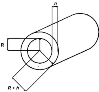
The RBM of nanotubes which interact with their surroundings can be modeled by two spring constants, one relating to the intrinsic properties of the nanotube (as stated in the last subsection), i.e., the C − C bond strength, and one relating to the interaction strength between the nanotube and its surroundings. If the RBM is modeled as a cylindrical shell (see Fig. 2.9) with one degree of freedom, x(t), which corresponds to the spatially uniform radial deflection from its equilibrium position, the Eq. 2.35 can be easily simplified. The RBM for the shell is therefore governed by:
x(t) R2 +
ρh
Eh(1−ν
2)∂2x(t)
∂t2 = 0, (2.38)
where where t is time, R is the radius, E is the Young’s modulus, ρ is the mass density per unit volume, ν is Poisson’s ratio, and h represents the thickness of the shell.
Comparing Eq. 2.38 to the standard equation of the harmonic oscillator:
∂2x(t)
∂t2 +ω
2x(t) = 0, (2.39)
we easily find that:
ω0 =
1 R
[
Eh
ρh(1−ν2)
]12
, (2.40)
which gives the radial breathing mode frequency for a cylinder free of external forces. Let us now suppose that a rigid shell, with radius Rs =R+s0, is concentrically coupled to
Figure 2.9: Schematics of the hollow cylinder with radius Rand thickness h. In the case of Single Wall Carbon Nanotubes,h is comparable to the diameter of a carbon atom.
The interaction between the cylinder’s wall and the rigid shell happens through Van der Waals forces, which are modeled by a Lennard-Jones potential given by:
U(x) =K
[
0.4
(
s0
s0+x
)10
−
(
s0
s0+x
)4]
, (2.41)
where s0 is the equilibrium separation with the cylinder. In the case that x(t) undergoes
small changes with relation to s0, the potential can be approximated by a expansion
around s0 giving:
U(x) =U0+
(
dU dx
)
so
(x−s0) +
1 2
(
d2U dx2
)
so
(x−s0)2+... . (2.42)
Note that this potential generates a restorative force (per unit of area) in the cylin-der’s wall. This force is given by the gradient of the potential given by Eq. 2.42:
p(x) = −∇U(x)≈ −2
(
d2U
dx2
)
so
(x−s0) =
24K s2
0
(x−s0), (2.43)
where the higher order terms were neglected. The cylindrical shell subjected to a pressure given by Eq. 2.43 is governed by:
x(t) R2 +
ρh
Eh(1−ν
2)∂2x(t)
∂t2 =−
(1−ν2)
Figure 2.10: A top view of the hollow cylinder surrounded by some medium. This medium forms a rigid shell around the cylinder whose radius is R +s0. The cylinder’s
wall interacts with the rigid shell by means of Van der Waals forces. The effect of such an interaction is upshifting the radial breathing mode frequency of the cylinder.
Rearranging Eq. 2.44 we find: ∂2x(t)
∂t2 +
Eh
ρh(1−ν2)
[
1 R2 +
24(1−ν2)
Eh
K s0
]
x(t) = 0. (2.45)
Finally, comparing Eq. 2.45 to Eq. 2.39 we find:
ω =
(
Eh
ρh(1−ν2)
)12 [ 1
R2 +
24(1−ν2)
Eh
K s0
]12
, (2.46)
which gives the new cylinder’s radial breathing mode frequency that is upshifted with respect toω0 given by Eq. 2.40. These findings will very important to explains the results
presented further in chapter 5.
2.2
Resonance Raman spectroscopy and SWNT
char-acterization
The Raman scattering, from a classical point of view, is related to the modulation of the polarizability α in the material by the vibrational mode Q. The electric dipole induced by the local fieldE⃗ can be described by:
⃗
where α is the electronic polarizability that, in general, depends on the generalized coor-dinate Q of a given vibrational mode. Expanding α in terms of Q, we have:
α =α0+
(
∂α ∂Q
)
0
Q+· · ·, (2.48)
where the derivative is made with relation to the equilibrium position. If ωq is the
fre-quency of the vibrational mode and ω0 is the frequency of the incident light, we can
rewrite E⃗ and Q as:
Q=Q0cosωqt and E⃗ =E⃗0cosω0t . (2.49)
Considering just small oscillations, the Eq. 2.47 is recapped as:
⃗
P =α0E⃗0cosω0t +
(
∂α ∂Q
)
0
Q0E⃗0cosω0t cosωqt. (2.50)
Using the trigonometric relation 2 cos(a) cos(b) = cos(a+b) + cos(a −b), the Eq. 2.50 becomes:
⃗
P =α0E⃗0cosω0t +
1 2 ( ∂α ∂Q ) 0
Q0E⃗0[cos(ω0−ωq)t + cos(ω0+ωq)t]. (2.51)
The first term in the Eq. 2.51 is related to the Rayleigh scattering. The components with frequencies (ω+ω0) e (ω−ω0) are related to the Raman scattering. Note that the Raman
scattering is possible only if
( ∂α ∂Q ) 0 ̸
= 0, (2.52)
which means that, in order to observe the Raman scattering, the polarizability must vary if the coordinate Q varies around the equilibrium. The Raman scattering is, therefore, the inelastic scattering of light.
Considering the quantum mechanics point of view, during a scattering event, (1) an electron is excited from the valence band to the conduction band by absorbing a photon, (2) the excited electron is scattered by emitting (or absorbing) phonons, and (3) the electron relaxes to the valence band by emitting a photon. If during the Raman process a phonon emission occurs, it means that a stokes process has taken place. Otherwise, if a phonon absorption occurs, it means that an anti-stokes process has happened [9]. The states |i⟩, |a⟩,|b⟩ e |f⟩ are defined as:
|i⟩ = |ni,0, n, ψ0⟩ (2.53)
|a⟩ = |ni−1,0, n, ψa⟩ (2.54)
|b⟩ = |ni−1,0, n±1, ψb⟩ (2.55)
where each ket contains information about the number of incident photons, the number of scattered photons, the number of phonons and the electronic state, respectively. The signal + stands for the Stokes process while the signal−stands for the anti-Stokes process. The figure 2.11 show the diagram of the Raman scattering Stokes process.
Figure 2.11: Diagram of the Raman scattering Stokes process. It worth to comment that, among the several possible diagrams for this process, this is the most likely one.
The energies associated to these states are:
Ei = ni~ωi+n~ωq+ε(v)(k0) (2.57)
Ea = (ni−1)~ωi+n~ωq+ε(c)a (k0) (2.58)
Eb = (ni−1)~ωi+ (n±1)~ωq+ε(c)b (k0) (2.59)
Ef = (ni−1)~ωi+~ωs+ (n±1)~ωq+ε(v)(k0) (2.60)
where ~ωq is the phonon energy, ~ωi is the incident photon energy, ~ωs is the scattered
photon energy, ε(v)(k
0) and ε(c)a,b(k0) are the energies of the electron in the valence and
the momentum, it follows that: ~ωi = ~ωs ±~ωq and ⃗ki = ⃗ks±⃗qq, where the ωq and
⃗qq are, respectively, the frequency and the wavevector of the phonon. ki and ks are the
wavevectors of the incident and scattered photons.
The number of emitted phonons before relaxation of the lattice can be one, two, and so on, which we call, respectively, one-phonon, two-phonon and multi-phonon Raman processes. The order of a scattering event is defined by the number of internal scattering events, including elastic scattering by an imperfection (such as a defect or an edge) of the crystal. The lowest order process is the first-order Raman scattering process which gives Raman spectra involving one-phonon emission. In graphene, the so-called G band around 1582 cm−1 is the only first-order Raman peak. In SWNTs, the G band spectra, which
is split into many features around 1580 cm−1, and the lower frequency radial breathing
mode (RBM) are usually the strongest features in SWNT Raman spectra, and they are both first-order Raman modes [9, 10].
Our target, the radial breathing mode, is a unique phonon mode,appearing only in carbon nanotubes and its observation in the Raman spectrum provides direct evidence that a sample contains SWNTs. Frequencies ωRBM raging from 50 to 500 cm−1 can be
expected. In fact, the radial breathing mode frequency ωRBM is the most important
SWNT spectroscopic signature because of its relation with SWNT diameter (dt) given
by ωRBM = 227/dt [34] (deviations from this relation can be attributed to
environmen-tal effects, as we will show in Chapter 5). These features make the resonance Raman spectroscopy a powerful tool to characterize SWNTs because, from a resonance Raman spectra (or a couple of them), we can extract information about EiiS,M and ωRBM. The
pair (EiiS,M, ωRBM) is unique for each SWNT specie and, with help of the Kataura’s plot,
it is possible to identify each (n, m). The Kataura’s plot bringsEiiS,M plotted as a function of dt (see Fig.2.12), which is linked to ωRBM through the relation ωRBM = 227/dt. Using
the dt(n, m) dependence given by Eq.2.2, it is possible to index a SWNT.
2.2.1
A guide to the Raman-based
(
n, m
)
assignment
The Raman-based (n, m) assignment is straightforward if the sample has isolated tubes or even bundles with small diameter tubes. In this case, the RBM spectra have well definedωRBM peaks [11, 13]. The (n, m) assignment becomes more difficult when the
sample is composed of SWNTs with a broad range of dt. The larger thedt, the larger the
overlap in the resonances among different RBMs for tubes of similar dt. In this case, the
Figure 2.12: The Kataura’s plot presents Eii as a function of dt. Each bullet represents
an uniqueEii from a given SWNT specie. Black bullets stand for metallic SWNTs, while
open bullets stand for semiconducting species. Using a pair (EiiS,M, ωRBM) experimentally
obtained and with help of the relation ωRBM = 227/dt we can run over all the SWNTs
presented in the plot, finding their (n, m) indices [11, 34, 35].
Let us begin with just one laser line. Figure 2.13(a) shows one RBM spectrum obtained using the 644 nm laser line (Elaser = 1.925 eV). Figure 2.13(b) shows the Kataura
plot used to analyze the spectra, obtained from Eq. 2.19 using the parameters for the “alcohol-assisted” CVD3grown SWNTs [13]. Each bullet represents one transition energy
(EiiM,S). From the bottom to the top, the first group is associated with the ES
22 (E11S is
below and only a single point can be seen at the right-bottom corner), the second group is the EM
11, the third group is the E33S, and so on. The light green bullets are associated
3
The nomenclatures “alcohol-assisted” (A.A) and “super-growth” (S.G.) carbon nanotubes will be employed throughout the text. The A.A. tubes are grown by CVD method using Acetate Cobalt-Molybdenum as percussor and alcohol as catalyst. During the growth process the CVD chamber is kept under a Ar/H2 flux. The S.G. tubes are grown by CVD method using Fecl3 (or Fe, Al/Fe, Al2O3/Fe,
Al2O3/Co ) as percussor and water as catalyst. During the growth process the CVD chamber is kept
Figure 2.13: (a) Raman spectrum (bullets) obtained with a 644 nm laser line. This spectrum was fitted by using 34 Lorentizians (curves under the spectra) and the solid line is the fitting result. (b) The Kataura plot from Eq. 2.19 with the parameters given in Ref. [13]. The dashed line indicates Elaser and the solid line gives the width of the
with semiconducting carbon nanotubes with mod(2n+m,3) = 1 (type one - SI), the olive bullets are associated with semiconducting carbon nanotubes with mod(2n +m,3) = 2 (type two - SII) and the red bullets are associated with metallic carbon nanotubes (mod(2n+m,3) = 0). In each group, we can realize several branches, called families, that are characterized by 2n+m =const. The geometrical patterns are crucial for the fitting (mainly in case one has a map with many laser lines), and they work for larger diameter tubes as well.
In Fig. 2.13(a) the bullets show the data and the solid line shows the fit obtained using 34 Lorentzian curves (the peaks bellow the spectral curve). Each Lorentzian curve can be related to one RBM from one carbon nanotube. The red Lorentzians represent the RBM from metallic tubes and the green (olive) Lorentzians represent the RBM from semiconducting SI (SII) tubes. To know how many Lorentzians should be used to fit each resonance spectrum, we use the Kataura plot. Figure 2.13(b) has a dashed line that represents the excitation energy for the spectrum shown in Fig. 2.13(a), and the two bold lines (above and below the dashed line) give the approximate boundary for the RBM resonance profiles [36]. To fit the spectrum shown in Fig. 2.13(a) we expect that all the circles inside the rectangle (Elaser ± 0.06) eV made by the two bold lines should show
up. The vertical bold lines connecting Fig. 2.13(a) and Fig. 2.13(b) indicate the metallic 2n+m = 30 family in resonance. Note that while the Kataura plot usually presentsEii as
a function ofdt, in Fig. 2.13(b), we plot Eiias a function of ωRBM for a direct comparison
with each spectrum. Here we have the first constraint:
• The conversion between ωRBM and dt must be performed considering the relation
(see Chapter 5) ωRBM = (227/dt)
√
1 +Ce·d2t. By properly adjusting the constant
Ce one can overlap the bullets in the Kataura’s plot within (Elaser ±0.06) eV and
RBM peaks in the spectrum.
The difficulty in performing the spectral fitting occurs because a large number of Lorentzian curves are needed to fit a broad RBM profile. The fitting program tends to broaden and increase some peaks, while eliminating others. If for the same fit, one Lorentzian is shifted by a couple of cm−1, the fitting program will return a completely
different fitting result. Therefore, another constraint, this time for the linewidths (full width at half maximum - FWHM), must be adopted:
Lorentzian peaks. Fluctuations of the RBM FWHM with (n, m) can be expected. However, such fluctuations do not change the picture of the results obtained after a self-consistent, many-cycles, fitting procedure.
After the fitting, one is ready to associate each pair (Elaser, ωRBM) with a specific
(n, m). With just one laser line (Elaser ±0.06) eV, the assignment procedure is reliable
enough to associate a given ωRBM to a couple (n, m) if the Eii values are well known.
However, a change in the environmental conditions (see Chapter 6) changes Eii and adds
uncertainty in energy. For those using just one laser line this uncertainty is accounted for considering that a change in the environment changes Eii by ∼ 40 meV in average,
although this value can go up to 100 meV (see Chapter 6), giving rise to a new freedom in the fitting [9, 11]. An additional anchor here, to decrease the uncertainty, is the fact that, as the chiral angle gets smaller (θ → 0), the Raman signal gets more intense [36]. In fact, the uncertainty in Eii is promptly overcome by using many laser lines, allowing
measurement of resonance profiles of each SWNT. After analyzing all the spectra obtained experimentally using the procedure described above for one laser line, we select each RBM frequency and plot its intensity as a function of Elaser. Such a plot gives the resonance
profile for the SWNT that has the specified RBM mode frequency. Figure 2.14 shows three Raman spectra for three Elaser values that are different but close to each other, so
that the same RBMs should be close to resonance for the three spectra. In each spectrum we selected two Lorentzian curves (with frequencies around 192 cm−1 and 186 cm−1) and
we show, in Figs. 2.14(d) and (e), their resonance profiles (Intensity vs Elaser). These
resonance profiles should then be fit by using the RRS intensity equation:
I(Elaser, Eq) =
M
(Elaser−Eii−iγ)(Elaser−Eii−Eq−iγ)
2 , (2.61)
where M represents the matrix elements, Elaser is the laser energy, Eii is the optical
transition energy, γ is the resonance window linewidth and Eq is the RBM energy. We
assume the matrix elements and γ do not change within one resonance profile. From the fits it is then possible to obtain the Eii for that specific RBM, i.e. for that specific (n, m)
SWNT.
2.3
Summary
Figure 2.14: Raman spectra (bullets) obtained with a (a) 630 nm, (b) 637 nm and (c) 644 nm laser lines. All the spectra are fit with a sum of Lorentizians (solid line). (d) The resonance profile for the carbon nanotube with ωRBM ∼ 192 cm−1, (n, m) = (12,6).
(e) The resonance profile for the carbon nanotube with ωRBM ∼ 186 cm−1, (n, m) =
Raman scattering. We also explained both, the electronic and the vibrational structure, emphasizing the importance of the circumferential confinement in the SWNT properties, where the most striking feature is the rising of the van Hove singularities. By means of the elasticity theory, an expression for the radial breathing mode frequency was deduced asωRBM = 227/dt. Next, a simple model based on van der Waals forces was employed to
explain how ωRBM changes with changing environment. In sequence, a brief introduction
Chapter 3
The Historical Overview of
E
ii
: van
Hove singularities, Excitons and the
Screening Problem
In this chapter, a summary of the historical evolution of the research behind theEii
is addressed. It is seen that Eii clearly depends on intrinsic and extrinsic properties (e.g.
a change in the environment). This dependence is attributed to the dielectric screening effect, which is connected to the dielectric constant κ. Usually, the excitonic transitions are calculated by means of the Bethe-Salpeter equation (see Chapter 2) and the dielectric screening within the random phase approximation (RPA). Finally, a simple method to describe κ is proposed.
3.1
The evolution of the experimental determination
of
E
iiAs briefly stated in Chapter 2, quantum confinement is responsible for the occur-rence of van-Hove singularities in the electronic structure of SWNTs, resulting in strong resonance processes. In general, the electronic density of states (DOS) is given by:
D(E) = 2 N
N
∑
µ=1
∫
1
dEµ(⃗k)
d⃗k
δ(Eµ(⃗k)−E)d⃗k . (3.1)
From Eq. 3.1 one can see that every time the derivative dEµ(⃗k)
d⃗k is equal to zero the
The last decade assembled much important experimental information about Eii
that, piece by piece, was supported by theoretical approaches by means of tight-binding and first-principles calculations [10, 12, 15, 16, 22, 23, 31, 37, 38]. In 2001, Jorio et al. [39] described Eii in terms of a first-neighbor tight-binding calculation combined with a
zone-folding procedure. They successfully explained their resonance Raman experimental results using this simple model because the range of tube diameters (1 < dt < 3 nm)
and laser energy (Elaser = 1.58 eV) covered a region where curvature and excitonic effects
were not evident [39]. In 2002, Bachilo et al. [40] performed Raman scattering and photoluminescence experiments on high-pressure carbon monoxide (HiPco) grown SWNTs dispersed in Sodium Dodecyl Sulfate (SDS) and, by analyzing the experimental ES
11 and
ES
22 values for semiconducting SWNTs, they figured out that the simple first-neighbor
tight-binding calculation was not able to accurately describe the experimental ES 11 and
ES
22 transition energies for SWNTs within the (0.7< dt<1.3 nm) range.
For this reason, the so-called “ratio-problem” and the curvature effect were intro-duced, providing evidence that excitons and the σ-π hybridization should be take into account. As explained in Chapter 2, Popov et al. [22, 37] and Samsonidze et al. [23] de-scribed the curvature effects using the ETB model, while Spataru et al. [38], performing first-principle calculations, described the exciton structure directly. The ETB model was efficient in describing all (2n+m)-family trends, as reported by Telget al.[41] and Fantini et al. [42]. Telg et al. and Fantini et al. used resonance Raman spectroscopy with a set of tunable lasers to map the RBM signal from HiPco SWNTs dispersed in SDS, building a 3D plot (see Fig. 3.1) from which they experimentally assigned more than 45 SWNTs, including S-SWNTs and M-SWNTs. Later, Wang et al. [29] and Maultzsch et al. [30] performed two-photons experiments giving rise to unquestionable experimental evidence that the electronic transitions in SWNTs arise from excitons.
In 2007, the RBM spectra of as-grown vertically aligned SWNTs synthesized by the chemical vapor deposition method from alcohol (theA.A.tubes previously described) were measured over a broad diameter (0.7 to 2.3 nm) and energy (1.26 to 2.71 eV) ranges [13]. Over 200 different SWNT species and about 380 different optical transition energies were probed, going up to the fourth optical transition of semiconducting SWNTs, thus establishing the (n, m) dependence of the poorly studied ES
33 and E44S transitions [13].
Over 95 different laser lines were used to generate the two-dimensional plot giving the Raman intensity as a function of the laser excitation energy (Elaser) and the inverse of
Raman frequency shift, as showed in Fig. 3.2. As stated in Chapter 2, the dt is known to
Figure 3.2: 95 different laser lines were used to generate a 2D color map showing the RBM spectral evolution as a function of excitation laser energy for SWNTs growth by the alcohol assisted CVD method. The intensity of each spectrum is normalized to the strongest peak, and we plot the inverse Raman shift. The Eii subbands are labeled with
S/M superscripts standing for semiconducting/metal tubes. [13]
can be directly related to a given SWNT diameter.
Using the 2D plot exhibited in Fig. 3.2, 84 different SWNTs species were unam-biguously indexed, allowing a careful analysis of Eii to be made from E22S to E44S. For
a fixed SWNT chirality, the Eii values are expected to exhibit a simple scaling behavior
(see Eq. 2.16 in Chapter 2) when plotted as a function of p/dt, where p = 1,2,3,4,5 for
ES
11, E22S,E11M,E33S, E44S, respectively [31].
Figure 3.3(a) shows a plot of the assigned transition energiesES
11,E22S,E11M,E33S,E44S
as a function ofp/dt, after correction for their chirality dependence obtained by
subtract-ing (βpcos 3θ/d2t) from the experimentally obtainedEiivalues (see inset to Fig. 3.3(a) and
respective caption forβp values, 1≤p≤5). Such a chirality correction is expected to
col-lapse allEii values onto a single (p/dt) dependent curve [31]. Note that the points do not
scale linearly as p/dt. As discussed by Kane and Mele [31] (and recapped in Chapter 2),
the non-linear scaling is due to many-body effects and can be fit with a logarithmic correc-tion (see Eq. 2.19). It is noticeable that theES
33andE44S transitions do not follow the same
scaling law as the ES
11 and E22S transitions, indicating that there is something
fundamen-tally different between the first two lowest energy optical transitions and the subsequent transitions in semiconducting SWNTs. Figure 3.3(b) shows evidence for the difference between the (ES
val-Figure 3.3: (a) Experimental optical transition energies obtained from analysis of Fig. 3.2 as a function of p/dt, after correcting for the chiral angle dependence (EiiEXP −
βpcos 3θ/d2t). The chirality dependence corrected E11S (black and white diamonds from
Ref. [40]), ES
22 (green/olive stars) and E11M (red stars) are fitted with Eq. (6.1). Inset:
the experimentalβp values for the lower (upper) Eiibranches are -0.07(0.05), -0.19(0.14),
-0.19(not measured), -0.42(0.42) and -0.4(0.4) forp= 1,2,3,4 and 5, respectively. (b) De-viation (∆E) of the (EEXP
ii −βpcos 3θ/d2t) data from the fitting curve in (a), versus 1/dt.
The solid line (∆E = 0.305/dt) fits the ∆E33S (green/olive circles) and ∆E44S (squares).
ues plotted in Fig. 3.3(a) can be fitted by [31] the Eq. 2.19 with 2aC−Cγ0 = 1.049 eV·nm,
b= 0.456 and c= 0.812 nm−1.
Figure 3.3(b) shows the deviation (∆E) of the chirality dependence corrected (Eii−
βpcos 3θ/d2t) values from the right side of Eq. (2.19). The deviations ∆E33S and ∆E44S from
the zero line in Fig. 3.3(b) shows a clear 1/dtdependence, and can be successfully fit by a
single expression ∆E =γ/dt, with γ = (0.305±0.004)eV·nm. Michelet al.[14] observed
the same odd behavior finding also a 1/dt dependent deviation.
3.2
The dielectric screening effect
The experimental evidences gave rise, so far, to the necessity of understanding how distinct states could shield each other, in the sense that this shielding could explain the scale break-down observed for ES
33 and E44S. Two approaches were made:
1. Quantum-chemistry calculations were used to explain the scaling-law breakdown showing that the excitons related to higher transitions (ES
33,E44S,) are weakly bound
(or are even unbounded e-h pairs) [13] due to the mixing of the DOS of ES 11 and
ES
22 with E33S. At the bottom of the E33S zone there is a large DOS from E11S and
ES
22, corresponding to delocalized and unbound states. This effect is enhanced at
the ES
33and E44S levels compared to the E22S states (the latter overlaps only with the
ES
11 band). The calculations estimate less than 0.001 eV separation in the density
of states at the ES
33 transition, attributed to other molecular states, compared to
about an 0.02 eV separation at the ES
22 transition. Any small perturbation (e.g.
dielectric environment inhomogeneity, tube ends or vibrational coupling) will mix the nearly isoenergetic states at theES
33 and E44S levels. Consequently the mixing of
all these states and non-Condon effects might become important with ES
33 and E44S
only marginally reflecting the character of “pure” states [13].