Thickness-dependent piezoelectric behaviour and dielectric properties
of lanthanum modiied BiFeO
3thin ilms
Glenda Biasotto
1, Francisco Moura
2, Cesar Foschini
1, Elson Longo
1, Jose A. Varela
1,
Alexandre Z. Simões
3,*1Universidade Estadual Paulista, UNESP - Instituto de Química, Laboratório Interdisciplinar em Cerâmica,
P.O. Box 355, 14801-907 Araraquara, São Paulo, Brazil
2Universidade Federal de Itajubá, UNIFEI - Campus Itabira, Rua São Paulo 377, Bairro Amazonas, P.O.
Box 355, 35900-37, Itabira, Minas Gerais, Brazil
3Universidade Estadual Paulista, UNESP - Faculdade de Engenharia de Campus Itabira, Av. Dr Ariberto
Pereira da Cunha 333, Bairro Pedregulho, P.O. Box 355, 12.516-410, Guaratinguetá, São Paulo, Brazil
Received 11 November 2010; received in revised form 4 March 2011; accepted 19 March 2011
Abstract
Bi0.85La0.15FeO3 (BLFO) thin ilms were deposited on Pt(111)/Ti/SiO2 /Si substrates by the soft chemical method. Films with thicknesses ranging from 140 to 280 nm were grown on platinum coated silicon substrates at 500°C for 2 hours. The X-ray diffraction analysis of BLFO ilms evidenced a hexagonal structure over the entire thickness range investigated. The grain size of the ilm changes as the number of the layers increases, indicating thickness dependence. It is found that the piezoelectric response is strongly inluenced by the ilm thickness. It is shown that the properties of BiFeO3 thin ilms, such as lattice parameter, dielectric permittivity, piezoeletric coeficient etc., are functions of misit strains.
Keywords: thin ilms, oxides, chemical syntheses, piezoelectricity
I. Introduction
Ferroelectromagnets are the class of materials ex-hibiting coexistence of magnetic and ferroelectric or-derings in a certain range of temperature [1–8]. It is known that relatively few multiferroic materials exist as naturally occurring phases, examples of which include
BiFeO3 (BFO) [9], BiMnO3 [10], TbMnO3 [11] and
Tb-Mn2O5 [12]. These materials, therefore, not only can be
used in magnetic and ferroelectric devices but also have the potential ability to couple the electric and magnet-ic polarizations, providing an additional degree of free-dom in device design and applications. Consequently, ferroelectromagnetism becomes the subject of intensive investigations because these materials potentially offer a whole range of applications, including the emerging
ield of spintronics [13], data-storage media [14] and
multiple-state memories [8]. These multiferroic materi-als have simultaneous ferromagnetic, ferroelectric and/
or ferroelastic ordering [15]. The ferroelectric mecha-nism in BFO is controlled by the sterochemical activity
of the Bi3+ 6s2 lone pair, responsible of a charge transfer
process from 6s2 to formally empty 6p orbitals [16,17]
while the weak ferromagnetic property can be
associat-ed with the residual moment from the cantassociat-ed Fe3+ spin
structure [18]. The coupling effect between both mag-netic and electric behaviours occurs through lattice dis-tortion of BFO [19] and Khomskii [20] has emphasized the different ways to combine magnetism and ferroelec-tricity in multiferroics materials.
Recently, large ferroelectric polarizations,
ex-ceeding those of prototypical ferroelectrics BaTiO3
and PbTiO3, have been reported in
heteroepitaxial-ly constrained BiFeO3 thin ilms [21–24]. Thus,
200-nm-thick BiFeO3 ilms, grown on (001)c, (110)c, and
(111)c SrTiO3 substrates with SrRuO3 as the bottom
electrode [21], have remanent polarizations of 55, 80,
and 100 µC/cm2, respectively. A 200-nm-thick BiFeO
3
ilm, grown on Si substrate with SrTiO3 as a template
layer [22], possesses a remanent polarization of 45 µC/ * Corresponding author: tel: +55 12 3123 2765
cm2. The piezoelectric constant d
33 shows a
dramat-ic increase from ~30 pm/V for a 100 nm ilm to ~120 pm/V for a 400 nm ilm. Wang et al. [23] reported a
re-manent polarization of 50–60 µC/cm2 in the
200-nm-thick BiFeO3 thin ilm grown by PLD onto the (100)
single crystal SrTiO3 substrate. They summarized that
the out of plane lattice parameter and the polarization
decrease while the piezoelectric coeficient increases as the ilm thickness increases. Catalan et al. [25] have shown that when bismuth ferrite is epitaxially grown
as a thin ilm onto, for example an SrTiO3 [001]
sub-strate, the resulting morphology is monoclinic, where the symmetry lowering distortion arises from in-plane contraction and out of- plane elongation as a result of
lattice mismatch between ilm and substrate.
In other work, Chu et al. [26] have evidenced BFO
ilm with a crystal structure of monoclinic phase,
which suggests that the polarization direction is close
to <111>. Such behaviour has also been conirmed by
piezoforce microscopy measurements. The authors have shown that ferroelectricity exists at a minimum
thickness down to 2 nm. Chu et al. [26] also probed
the role of La substitution on the ferroelectric
proper-ties of epitaxial BiFeO3 ilms on SrTiO3-templated Si.
This provides a mechanism to engineer the rhombohe-dral distortion in the crystal and, thus, control domain
structure and switching. With the 10 at.% La substi
-tution, the (Bi0.9La0.1FeO3) ilm showed well-saturated
ferroelectric hysteresis loops with a remanent
polar-ization of 45 µC/cm2, a converse piezoelectric coefi
-cient d33 of 45 pm/V, and a dielectric constant of 140.
Over this range of La substitution, the coercive ield
systematically decreases in such a way that a coercive
voltage of 1 V can be obtained in a 100 nm thick ilm.
These results show promise for the ultimate implemen-tation of this lead-free multiferroic operating at voltag-es in the range of 2–3 V [27]. Zechvoltag-es et al. [28] using a combination of epitaxial growth techniques in con-junction with theoretical approaches, have shown the formation of a morphotropic phase boundary through epitaxial constraint in lead-free piezoelectric bismuth
ferrite (BiFeO3) ilms. Electric ield-dependent stud
-ies show that a tetragonal-like phase can be reversibly converted into a rhombohedral-like phase, accompa-nied by measurable displacements of the surface, mak-ing this new lead-free system of interest for probe-based data storage and actuator applications.
A tetragonal-like crystal structure with c axis nor-mal to the substrate surface with a snor-mall monoclin-ic distortion of about 0.5° was observed by four-cycle X-ray diffraction [24]. However, a more recent study made by Eerenstein et al. [29] argues that the compres-sive epitaxial strain does not enhance the
magnetiza-tion and ferroelectric polarizamagnetiza-tion in BiFeO3 thin ilm.
Soon after, Wang et al. [30] immediately report the
re-sults of additional experiments on this issue. The mag-netization of about ~0.5 µB per unit cell for very thin
ilm, although smaller than that in the original magnet
-ic measurement of Wang et al. [30], is still much
great-er than that reported by Egreat-erenstein et al. [29], which
also progressively decreases as the ilm thickness is in -creased to above 120 nm. They suggest that the effect of epitaxial strain can-not be completely ruled out and some additional possible reasons for obtained results are proposed.
If the capacitor area is comparable to the grain size
of ferroelectric thin ilms or electrodes, the inluence
of grain size and grain boundary cannot be neglected
and ferroelectric ilms and electrodes are required to
be thin. For this reason, it is necessary to investigate
the inluence of grain size, grain boundary and thick -ness on the electrical properties. The size effects of thin
ilms are different from that of bulk materials. Size ef
-fects of thin ilms include not only grain size but also ilm thickness. It is dificult to distinguish the size ef -fects derived from grain size from those derived from
ilm thickness because the grain size of the thin ilms generally changes with ilm thickness if ilms are pre -pared by chemical solution deposition [31].
Further-more, it has also been reported that the ilm thickness dependence of a polycrystalline ilm is different from that of epitaxially grown ilms [32]. The effect of stress
and the existence of a low dielectric constant
interfa-cial layer between the ferroelectric thin ilm and the
substrate are noted to explain these phenomena [33]. In the present investigation and as a natural
exten-sion of previous work, Bi0.85La0.15FeO3 thin ilms were
prepared on Pt(111)/Ti/SiO2/Si substrates by the soft
chemical method. Structural and electrical properties
of the ilms, mainly related to strain behaviour were in -vestigated by using various techniques with an aim to explore their technological applications [34,35].
However, there are no evidences in the literature
showing the inluence of the Bi0.85La0.15FeO3 (BLFO)
ilm (obtained by the polymeric precursor method)
thickness on the ferroelectric properties [34]. In this ar-ticle, we report the dependence of the electrical
proper-ties from the thickness of BLFO thin ilms deposited on
Pt(111)/Ti/SiO2/Si substrates by the soft chemical
meth-od. The inluence of BLFO ilms thickness on leakage
behaviour is also discussed.
II. Experimental
Lanthanum modiied bismuth ferrite thin ilms were
prepared by the soft chemical method, as described
elsewhere [36]. The ilms were spin coated on Pt/Ti/
SiO2/Si substrates by a commercial spinner operating
at 5000 revolutions/min for 30 s (spin coater KW-4B, Chemat Technology). An excess of 5 wt.% of Bi was
added to the solution aiming to minimize the bismuth
annealed at 500°C for 2 hours in the conventional
fur-nace under static air atmosphere. The ilm thickness was
reached by repeating 6, 8 and 10 times the spin-coating and heating treatment cycles. The thickness of the
an-nealed ilms was measured using scanning electron mi -croscopy (Topcom SM-300) at the transversal section
and back-scattering electrons. We have obtained ilms
with the thicknesses in the range of 140 to 280 nm.
Phase analysis of the ilms was performed at room temperature by X-ray diffraction (XRD) using a Bragg- Brentano diffractometer (Rigaku-DMax 2500PC) and Cu-Kα radiation. Raman measurements were per -formed using an ISA T 64000 triple monochromator. An optical microscope with 80× objective was used to focus the 514.5 nm radiation from a Coherent Innova
99 Ar+ laser on the sample. The same microscope was
used to collect the back-scattered radiation. The dis-persed scattering light was detected by a
charge-cou-pled device (CCD) detection system. Surface rough -ness (RMS) and average grain size was examined by AFM, using tapping mode technique. Next, a 0.5 mm diameter top Au electrode was sputtered through a shadow mask at room temperature. After deposition of
the top electrode, the ilm was subjected to a post-an -nealing treatment in a tube furnace, at 300°C with con-stant heating rate of 1°C/min, in oxygen atmosphere for 1 hour. The aim was to decrease eventually present oxygen vacancies. The leakage current-voltage (I-V) characteristic was determined with a voltage source measuring unit (Radiant Technology 6000 A). Piezo-electric measurements were carried out using a setup based on an atomic force microscope in a Multimode Scanning Probe Microscope with Nanoscope IV con-troller (Veeco FPP-100). In our experiments,
piezore-sponse images of the ilms were acquired in ambient
air by applying a small ac voltage with amplitude of 2.5 V (peak to peak) and a frequency of 10 kHz while
scanning the ilm surface. To apply the external volt
-age we used a standard gold coated Si3N4 cantilever
with a spring constant of 0.09 N/m. The probing tip, with an apex radius of about 20 nm, was in
mechani-cal contact with the uncoated ilm surface during the
measurements. Cantilever vibration was detected us-ing a conventional lock-in technique. All measure-ments were performed at room temperature.
III. Results and discussion
It is well known that the properties of ilms are sig
-niicantly affected by the orientation of the underlying layer, ilm thickness and atmosphere low. It is impor -tant to control the thickness of the layer due to its strong
inluence on the grain size, dielectric and ferroelectric properties. For thinner ilms interfacial “dead layers”
which possess poor dielectric properties could appear
at the interface ilm-substrate inluencing on the ilms
performance. These dead layers are originated from
ox-ygen interdiffusion, chemical reaction, or structural
de-fects and can be suppressed when ilm is thicker than 200 nm. Thus, ilms with 6, 8 and 10 layers were depos
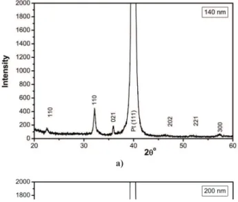
-ited on platinum coated silicon substrates and the XRD pattern is illustrated in Fig. 1. The ilms were well crys -tallized at a processing temperature of 500°C. This tem-perature was chosen because in previous work we have demonstrated that a pure perovskite phase is formed at 500°C for 2 hours with no second phases detected [37]. The characteristic peak for platinum coated silicon (111)
substrates was observed in the range of 38° < 2θ < 44°.
a)
b)
c)
Figure 1. XRD patterns for BLFO ilms with different thick
All ilms exhibit a polycrystalline structure, except the 280 nm thick ilms which show (10l)-randomly ori
-ented crystals. Thicker BLFO ilm consists of random -ly oriented perovskite phase. Some orientation-sen-sitive physical properties, such as dielectric constant, remanent polarization and drive voltage, should vary with the extent of mixed orientations which are
differ-ent for the ilms grown with differdiffer-ent number of layers.
The discussed preferred orientations can be induced by strain due to the differences in lattice parameters and
thermal expansion coeficients between BLFO and Pt
substrate, indicating that the polar axis is closer to (101)
than (110). The diffraction peaks of thicker BLFO ilms
are sharper and stronger than those of thinner BLFO
ilms, indicating better crystallization. XRD results
show that the crystalline quality is improved by the
in-creasing thickness of thin ilms. Although all the ilms
were processed under the same conditions, the thicker
ilms possess better crystallinity because there is a large
amount of material deposited on substrate surface
in-luencing the appearance of higher intensities diffrac -tion peaks.
The thickness dependence of the a and c lattice
con-stants and unit cell volume of the ilms is shown in Ta
-ble 1. In this study, we have adopted the Rietveld reine -ment technique to investigate the crystal structure of the
BLFO system. The data were collected from the ilms
annealed at 500°C for 2 hours while clear evidence for the preferred site for lanthanum substitution was
ob-tained. Table 1 illustrates the Rwp, Rexp, and S indexes,
as well as the lattice parameters (a and c) and the unit cell volume (V). The atomic positions obtained by
Riet-veld analyses belong to the ICSD card (PDF # 71-2494)
with hexagonal symmetry. The quantitative phase anal-yses for the tetragonal phase were calculated according
to the reference of Young et al. [38]. BLFO ilms had
a hexagonal structure over the entire thickness range
investigated. In addition, the ilms are polycrystalline without epitaxy along speciic orientation. The differ -ence in crystalline properties and inner stress between
BLFO ilms on platinum coated silicon substrates orig -inates from the difference in the lattice mismatch, the
thermal expansion coeficient and the crystalline struc -ture. The strain formed is generally released by forming
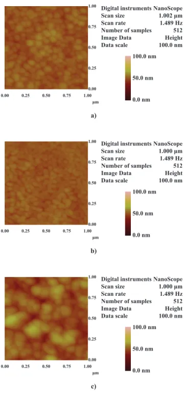
Figure 2. AFM images of BLFO ilms with different thicknesses: a) 140 nm, b) 200 nm and c) 280 nm
Table 1. Dependence of a and c lattice constants and unit cell volume for BLFO thin ilms as a function of thickness
Reinement indexes
Parameters 140 200 280
(nm) (nm) (nm)
RWP (%) 10.19 10.78 12.57
REXP 7.02 6.60 9.00
S 1.44 1.62 1.39
Lattice parameters
a (Å) 5.5879 5.5942 5.6011
c (Å) 13.6066 13.6386 13.6429
V (Å3) 367.94 369.64 371.01
Digital instruments NanoScope
Scan size 1.002 μm
Scan rate 1.489 Hz
Number of samples 512
Image Data Height
Data scale 100.0 nm
100.0 nm
50.0 nm
0.0 nm
1.00
0.75
0.50
0.25
0.00 0.00 0.25 0.50 0.75 1.00
a) μm
Digital instruments NanoScope
Scan size 1.000 μm
Scan rate 1.489 Hz
Number of samples 512
Image Data Height
Data scale 100.0 nm
100.0 nm
50.0 nm
0.0 nm
1.00
0.75
0.50
0.25
0.00 0.00 0.25 0.50 0.75 1.00
b) μm
Digital instruments NanoScope
Scan size 1.000 μm
Scan rate 1.489 Hz
Number of samples 512
Image Data Height
Data scale 100.0 nm
100.0 nm
50.0 nm
0.0 nm
1.00
0.75
0.50
0.25
0.00 0.00 0.25 0.50 0.75 1.00
disorders at the interface and grain boundaries. This is
reasonable since in the thin ilm form, not only La sub -stitution but also the in-plane stress has effects on the
structure [39,40]. The obtained results conirmed that
the Bi+3 ion was substituted by the La+3 ion in the BFO
phase and no changes occurred in the reinements. It
was observed that La3+ substitutes Bi3+ only in a
per-ovskite-type unit cell, causing a distorted structure. The covalent interaction, which originates from the strong hybridization between Fe 3d and O 2p orbitals, plays an important role in the structural distortion of BLFO
lat-tice. Doping with La improves oxygen ion stability in
the lattice because some of the Bi ions in the pseudo-perovskite layers containing Fe-O octahedra were
sub-stituted by the rare earth ion. From the low S values
(S = Rwp/Rexp) it can be assumed that the reinement was
successfully performed with all the investigated param-eters close to literature data [41].
Figure 2 presents the AFM images of the ilms with
different thicknesses. A strongly marked difference in
the ilm microstructure can be observed for different numbers of layers. When the ilm thickness increased,
distinctive plate-like grains were clearly observed. The
absence of cracks and issures indicates that the ilm has a uniform microstructure. The thinner ilms present a
dense and granular microstructure. The difference in the shape of the grains is related to the amount of materi-al deposited on the substrate surface to crystmateri-allize the
ilms. Thinner ilms possess less material to be crystal -lized and the grains tend to assume the rounded shape
(more energetic). Meanwhile, when the ilm thickness
increased, a large amount of material to be crystallized may lead to elongated grains (a less energetic). The
sur-face roughness was dependent on the ilm thickness as
well as the grain size changing from 53 to 130 nm as the number of layers is increased. Considering that the
fer-roelectric properties of the BLFO thin ilms are strongly inluenced by the ilm microstructure, i.e., by the grain
size, we expect that, in our case, electrical properties
will be sensitive to ilm thickness. The surface morphol
-ogy of the BLFO ilms on Pt/Ti/SiO2/Si substrates
deter-mined by atomic force microscopy (AFM) is shown in
Fig. 3. Surface roughness increases with ilm thickness. The root-mean-square (RMS) roughness of the ilms is 2.8, 11.0 and 14.0 nm, respectively, for the BLFO ilms
280, 200 and 140 nm thick. Higher RMS value was
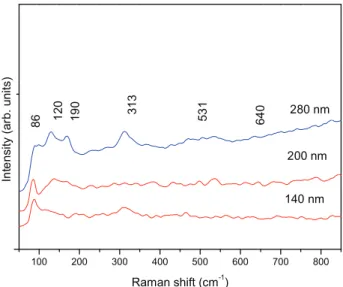
ob-served in thicker ilms caused by their larger grains. Raman analysis in the lanthanum modiied bismuth
ferrite shows the order-disorder degree of the atom-ic structure at short range (Fig. 3). The modes further split into longitudinal and transverse components due the long electrostatic forces associated with lattice io-nicity. Lanthanum atoms substitute bismuth within the
perovskite structure having marginal inluence in the in
-teractions between the (Bi2O2)2+ layers and perovskite.
The vibrational modes located at 313, 531 and 640 cm-1
result from the FeO6 octahedral (Fe = 5 or Fe = 6). The
band located below 200 cm-1 is due to the different sites
occupied by bismuth within the perovskite layer. As the
ilm becomes thinner, vibrational modes tend to dis -appear, indicating high structural disordering at short range in the crystal structure as well as the poor
crys-tallinity of the ilm. A minimum disorder was obtained for the 280 nm thick ilm while the highest disorder cor -responds to a minimum thickness value. The origin of
disorder in the BLFO thin ilms is addressed to the lat -tice distortion. The suppressed lat-tice distortion might
also cause internal strain in the ilm as observed in the thicker ilm. However, near a thickness of 280 nm the
lattice distortion is reduced indicating that the driving force for the internal strain was minimized. The reason is that the internal strain changes the microstructure of
BLFO ilms. High internal strains correspond to small -er and coarse grains and, as a result, provide an increase
in the number of grain boundaries. Thinner ilms pres -ent large amount of defects associated to the disorder in the BLFO lattice.
The disorder developed in the ilm is strongly de -pendent on the thickness showing that the amount of material deposited on the surface of substrate causes a reduction in the defects or disorder of materials. Con-sidering that the ferroelectric properties of BLFO thin
ilms are strongly inluenced by ilm microstructure,
i.e., by the grain size, we expect that, in our case,
piezo-electric properties will be sensitive to ilm thickness.
Figure 4 shows the leakage current density as a
func-tion of ilm thickness. The leakage current density at 1.0 V for the 140-nm-thinner ilm was in the order of 10-6
A/cm2, but it decreased to the order of 10-7 A/cm2 for
thicker ilms. The lower leakage current observed for thicker ilms may be probably attributed to differences
in grain size, density and surface structure due to
differ-100 200 300 400 500 600 700 800
6
4
0
5
3
1
3
1
3
1
9
0
1
2
0
8
6
140 nm 200 nm 280 nm
In
te
n
s
it
y
(
a
rb
.
u
n
it
s
)
Raman shift (cm-1)
Figure 3
Figure 3. Micro-Raman spectra for BLFO ilms with different thicknesses: a) 140 nm,
36
ences in the number of layers. Since the thinner BLFO
ilms possess higher leakage currents than the thicker ones less resistive ilms are expected. Two clearly dif -ferent regions were evident. The current density
in-creases linearly with the external electric ield in the re
-gion of low electric ield strengths, suggesting an ohmic conduction. At higher ield the current density increas -es exponentially, which impli-es that at least one part of the conductivity results from Schottky or
Poole-Fren-kel emission mechanisms. The symmetric J–V curves
were attributed to bulk-limited leakage behaviour rath-er than intrath-erface-limited leakage behaviour in a previ-ous work [42].
The dielectric permittivity and the dissipation factor
as a function of ilm thickness are presented in Fig. 5.
The dielectric measurements were carried out at room temperature as a function of frequency in the range
from 10 kHz to 1 MHz. The igures show that both di -electric permittivity and the dissipation factor of almost
all BLFO ilms remain fairly constant in this frequen
-cy range. The value of εr decreases from 220 to 100
when the ilm thickness decreases from 280 to 140 nm.
This shows that dead layers with lower dielectric
con-stant are formed between the BLFO ilms and Pt elec
-trodes. Because dead layers and the BLFO ilms are in
series in the capacitance structure, the dielectric
permit-tivity is reduced with decreasing the BLFO ilm thick
-ness. The tan δ changes slightly with increase
thick-ness of the BLFO ilm. The εr and tan δ values are
(100, 0.021), (160, 0.017) and (220, 0.024),
respective-ly, for the BLFO ilms with thickness of 140, 200 and
280 nm. As it can be seen, the dielectric permittivity shows very little dispersion with frequency indicating
that the ilms possess low defect concentrations at the interface ilm-substrate. The low dispersion of the di -electric permittivity and the absence of any relaxation
peak in tan δ indicate that an interfacial polarization of
the Maxwell Wagner type and an interfacial polariza -tion arisen from the electrode barrier are negligible in
the ilm. The BLFO ilm had higher relative dielectric
permittivity when compared to those previously
report-ed in ceramics or ilms [43–49]. The observreport-ed improve -ment of dielectric permittivity may be associated with less structural disorder and less two-dimensional stress
in the plane of the ilm.
The piezoelectric behaviour at room temperature is
shown in Fig. 6. Butterly-shaped piezoelectric coefi
-cient versus electric ield can be observed for different ilm thickness. The difference in the piezoelectric be
-haviour might be attributed to different domain conigu
-rations. As usually observed in the relaxor-based “soft” piezoelectric materials, the hysteresis at low ields is
attributed to domain motions. In the present work, the hysteresis could also be associated with the domain re-orientation, which is prominent for a sample with a multidomain state. Above 30 kV/cm, the hysteresis-free
strain is observed, implying a poling state free of do-main wall motions induced by the high external
elec-tric ields. At 60 kV/cm, the highest elecelec-tric ield in the work, the piezoelectric coeficient is maximum. The thicker ilm has a higher piezoelectric behaviour in part
due to domain reorientation in which a large grain with a multi domain- structure has a higher mobility for polar-ization reversal than a small grain with a single-domain-structure. Beyond that point, it is possible that a
mod-0,1 1 10
10-8 10-7
10-6
10-5 10-4
10-3 140 nm
L e a k a g e C u rr e n t d e n s it y ( A /c m 2 ) Voltage (V)
Figure 4.
0,1 1 10
10-6 10-5 10-4 200 nm L e a k a g e C u rr e n t d e n s it y ( A /c m 2 ) Voltage (V)
Figure 4.
0.1 1 10
1 0-7
1 0-6 1 0-5 1 0-4
1 0-3
1 0-2
1 0-1 100
28 0 n m
L e a k a g e C u rr e n t D e n s it y ( A /c m 2 )
Volta ge (V )
Figure 4.
Figure 4. Leakage current density versus applied electric ield for BLFO ilms with different thicknesses:
a) 140 nm, b) 200 nm and c) 280 nm
a)
b)
c)
37
est bias ield results in the transition from asymmetric to symmetric phase. This ield-induced phase transition
may be ascribed to the pinching effect, that is, the con-sequent decrease in free energy difference among
poly-morphic phases. A careful inspection of the d33 - E plots
reveals that there are two apparent linear regions at low
ields (E < 30 kV/cm) and high ields (E > 70 kV/cm) and one transition region. That corresponds to domains
reorientation induced by external electric ields. It is
shown that the thicker ilm exhibited higher piezoelec
-tric strain than the thinner one. The piezoelec-tric coefi -cient was 43 pm/V, 40 pm/V and 30 pm/V for the BLFO
ilmswith ilm thickness of 280, 200 and 140 nm, re -spectively. The improvement of piezoelectric response
for the thicker ilm can be caused by the lower struc -tural disorder and the lower two-dimensional stress in
the plane of the ilm as well as differences in grain size,
density and surface structure [50].
Figure 5. Dielectric permittivity and dielectric loss spectra of BLFO thin ilms with different thicknesses:
a) 140 nm, b) 200 nm and c) 280 nm
Figure 6. Piezoelectric coeficient for BLFO ilms with different thicknesses: a) 140 nm,
b) 200 nm and c) 280 nm
a) a) b) b) c) c)
0 200
101 102 103
0,0 0,2 0,4 0,6 0,8 1,0 ta n 280 nm D ie le tr ic C o n s ta n t ( ) Frequency (kHz)
Figure 5.
101 102 103
0 200 0,0 0,1 0,2 0,3 200 nm D ie le tr ic C o n s ta n t ( ) ta n
(b)
Figure 5.
0,0 0,1 0,2 0,3 ta n Figure 5.
200 D ie le tr ic C o n s ta n t ( ) Figure 5.
Frequency (kHz) 0,0 0,2 0,4 0,6 0,8 101 102 103 0 200 ta n 140 nm D ie le tr ic C o n s ta n t ( ) Frequency (kHz)Figure 5.
-70 0 70
0 20 40 60 140 nm d3 3 ( p m /V )
Electric Field (kV/cm)
d
/V
)
Figure 6.
-60 -45 -30 -15 0 15 30 45 60
0 20 40 200 nm d33 ( p m /V )
Electric Field (kV/cm)
Figure 6.
-70 0 70
0 30 60
d33
(
p
m
/V
)
Electric Field (kV/cm)
280 nm
IV. Conclusions
The thickness effect on piezoelectric properties of Bi0.85La0.15FeO3 (BLFO) thin ilms fabricated by the soft
chemical method was investigated. BLFO ilms had a
hexagonal structure over the entire thickness range
in-vestigated. The thinner ilms possess a dense and granu
-lar microstructure, whereas the thicker ilms have grain
aggregation morphology and randomly oriented
per-ovskite phase. The thinner ilm tends to increase the leak -age current as well as decrease the dielectric constant
and piezoelectric coeficient due to the internal strain re -sulting from the electrode/ferroelectric interfacial layer.
The optimal ilm thickness is close to 280 nm. The re -sults of these studies are very promising and suggest that
the BLFO thin ilms can be used as a storage element in
nonvolatile ferroelectric random access memories.
Acknowledgements: The authors gratefully
acknowl-edge the inancial support of the Brazilian inancing
agencies FAPESP, CNPq and CAPES.
References
N.A. Spaldin, M. Fiebig, “The Renaissance of Mag -1.
netoelectric Multiferroics”, Science, 309 (2005) 391– 392.
W. Eerenstein, N.D. Mathur, J.F. Scott,” Multiferroic
2.
and Magnetoelectric Materials”, Nature, 442 (2006) 759–765.
S.W. Chong, N. Mostovoy, “A magnetic twist for fer -3.
roelectricity”, Nat. Mater., 6 (2007) 13–20.
R. Ramesh, N.A. Spaldin, “Multiferroics: progress
4.
and prospects in thin ilms”, Nat. Mater., 6 (2007) 21– 29.
W. Eerenstein, M. Wiora, J.L. Prieto, J.F. Scott, N.D.
5.
Mathur, “Giant sharp and persistent converse magne -toelectric effects in multiferroic epitaxial
heterostruc-tures”, Nat. Mater., 6 (2007) 348–356.
M. Fiebig, “Revival of the magnetoelectric effect”
6. J.
Phys. D., 38 (2005) R123–R152.
G. Catalan, “Magnetocapacitance without magne -7.
toelectric coupling”, Appl. Phys. Lett., 88 (2006) 102902–102904.
N.A. Hill, “Why are there so few magnetic ferroe -8.
lectrics?”, J. Phys. Chem. B., 104 (2000) 6694–6709. A.H.M. Gonzalez, A.Z. Simões, L.S. Cavalcante, E. 9.
Longo, J.A. Varela, C.S. Riccardi, “Soft chemical
deposition of BiFeO3 multiferroic thin ilms”, Appl.
Phys. Lett., 90 (2007) 052906–052908.
A.M. dos Santos, S. Parashar, A.R. Raju, Y.S. Zhao, 10.
A.K. Cheetham, C.N.R. Rao, “Evidence for the like -ly occurrence of magnetoferroelectricity in the
sim-ple perovskite, BiMnO3”, Solid State Commun., 122
(2002) 49–52.
T. Kimura, T. Goto, H. Shintani, K. Ishizaka, T. Ari-11.
ma, Y. Tokura, “Magnetoelectric phase diagrams
of orthorhombic RMnO3”, Phys. Rev. B., 71 (2005)
224425–224236.
N. Hur, S. Park, P.A. Sharma, J.S. Ahn, S. Guha, S.W.
12.
Cheong, “Electric polarization reversal and memory in a multiferroic material induced by magnetic ields”,
Nature, 429 (2004) 392–395.
H. Bea, M. Bibes, M. Sirena, G. Herranz, K. Bouze-13.
houane, E. Jacquet, S. Fusil, P. Paruch, M. Dawber, J.P. Contour, A. Barthelemy, “Tunnel magnetoresist -ance and robust room temperature exchange bias with
multiferroic BiFeO3 epitaxial thin ilms”, Appl. Phys.
Lett., 90 (2006) 062502–062504.
M. Fiebig, Th. Lottermoser, D. Frhlich, A.V. Golsev,
14.
R.V. Pisarev, “Observation of coupled magnetic and electric domains”, Nature, 419 (2002) 818–820.
H. Schmid, “On the birefringence of magnetoelectric
15.
BiFeO3”, Ferroelectrics., 204 (1994) 23–33.
R. Seshadri, N.A. Hill, “Visualizing the role of Bi 6s
16.
“lone pairs” in the off-center ferromagnetic BiMnO3”,
Chem. Mater., 13 (2001) 2892–2899.
T. Shishidou, N. Mikamo, Y. Uratani, F. Ishii, T. 17.
Oguchi., “First-principles study on the electronic structure of bismuth transition-metal oxides”, J. Phys.
Condens. Matter., 16 (2004) S5677–S5683.
P. Fischer, M. PoIomska, I. Sosnowskag, M. Szy-18.
manskig, “Temperature dependence of the crystal and
magnetic structures of BiFeO3”, J. Phys. C.: Solid
State Phys., 13 (1980) 1931–1937.
S-W. Cheong, M. Mostovoy, “Multiferroics: a mag -19.
netic twist for ferroelectricity”, Nat. Mater., 6 (2007) 13–20.
D.I. Khomskii, “Multiferroics: Different ways to com -20.
bine magnetism and ferroelectricity”, J. Magn. Magn. Mater., 360 (2006) 1–8.
J.F. Li, J. Wang, M. Wuttig, R. Ramesh, N. Wang,
21.
B. Ruette, A.P. Pyatakov, A.K. Zvezdin, D. Vieh
-land, “Dramatically enhanced polarization in (001),
(101), and (111) BiFeO3 thin ilms due to epitiax
-ial-induced transitions”, Appl. Phys. Lett., 84 (2004) 5261–5263.
J. Wang, H. Zheng, Z. Ma, S. Prasertchoung, M. Wut -22.
tig, R. Droopad, J. Yu, K. Eisenbeiser, R. Ramesh, “Epitaxial BiFeO3 thin ilms on Si”, Appl. Phys. Lett.,
85 (2004) 2574–2576.
Y. Lin, A. Boker, Q. Wang, S. Long. K. Sill, A. Balazs,
23.
T.P. Russel, “Self-directed self-assembly of nanoparti
-cle/copolymer mixtures”, Science, 434 (2005) 55–59.
F. Bai, J. Wang, M. Wuttig, J.F. Li, N. Wang, A.P. Py -24.
atakov, A.K. Zvezdin, L.E. Cross, D. Viehland, “De
-struction of spin cycloid in (111)c-oriented BiFeO3
thin ilms by epitiaxial constraint: Enhanced polariza
-tion and release of latent magnetiza-tion”, Appl. Phys.
Lett., 86 (2005) 032511–032513.
G. Catalan, J.F. Scott, “Physics and applications of
25.
bismuth ferrite”, Adv. Mater., 21 (2009) 2463–2485. Y.H. Chu, T. Zhao, M.P. Cruz, Q. Zhan, P.L. Yang, 26.
L.W. Martin, M. Huijben, C.H. Yang, F. Zavaliche, H. Zheng, R. Ramesh, “Ferroelectric size effects in
multiferroic BiFeO3 thin ilms”, Appl. Phys. Lett., 90
Y.H. Chu, Q. Zhan, C.-H. Yang, M.P. Cruz, L.W. Mar -27.
tin, T. Zhao, P. Yu, R. Ramesh, P.T. Joseph, I.N. Lin,
W. Tian, D.G. Schlom, “Low voltage performance of
epitaxial BiFeO3 ilms on Si substrates through lan
-thanum substitution”, Appl. Phys. Lett., 92 (2008) 102909–102911.
R.J. Zeches, M.D. Rossell, J.X. Zhang, A.J. Hatt, Q.
28.
He, C.-H. Yang, A. Kumar, C.H. Wang, A. Melville,
C. Adamo, G. Sheng, Y.-H. Chu, J.F. Ihlefeld, R. Erni,
C. Ederer, V. Gopalan, L.Q. Chen, D.G. Schlom, N.A. Spaldin, L.W. Martin, R. Ramesh, “A strain-driven
morphotropic phase boundary in BiFeO3”, Science,
326 (2009) 977–980.
W. Eerenstein, F.D. Morrison, J. Dho, M.G. Blamire,
29.
J.F. Scott, N.D. Mathur, Comment on “Epitaxial
BiFeO3 multiferroic thin ilm heterostructures”,
Sci-ence, 307 (2005) 1203a.
J. Wang, A. Scholl, H. Zheng, S.B. Ogale, D. Vieh -30.
land, D.G. Schlom, N.A. Spaldin, K.M. Rabe, M. Wuttig, L. Mohaddes, J. Neaton, U. Waghmare, T. Zhao, R. Ramesh, Response to Comment on “Epi
-taxial BiFeO3 multiferroic thin ilm heterostructures”,
Science, 307 (2005) 1203b.
A.Z. Simões, M.A. Ramirez, N.A. Perucci, C.S. Ri-31.
ccardi, E. Longo, J.A. Varela, “Retention character -istics in Bi3.25La0.75Ti3O12 thin ilms prepared by the
polymeric precursor method”, Appl. Phys. Lett., 86 (2005) 112909–112911.
T. Hayashi, N. Oji, H. Maiwa, “Film thickness de -32.
pendence of dielectric properties of BaTiO3 thin ilms
prepared by sol-gel method”, Jpn. J. Appl. Phys., 33
(1994) 5277–5280.
J.F.M. Cillessen, M.W.J. Prins, R.W. Wolf, “Thickness
33.
dependence of the switching voltage in all-oxide
fer-roelectric thin-ilm capacitors prepared by pulsed la
-ser deposition”, J. Appl. Phys., 81 (1997) 2777–2781. A.Z. Simoes, A.H.M. Gonzalez, C.S. Riccardi, E.C. 34.
Souza, F. Moura, M.A. Zaghete, E. Longo, J.A.
Vare-la, “Ferroelectric and dielectric properties of lantha
-num modiied bismuth titanate thin ilms obtained by the polymeric precursor method”, J. Electroceram.,
13 (2004) 65–70.
A.Z. Simões, B.D. Stojanovic, M.A. Zaghete, C.S.
35.
Riccardi, A. Ries, F. Moura, E. Longo, J.A.Varela,
“Electrical characterization of lanthanum-modiied bismuth titanate thin ilms obtained by the polymer
-ic precursor method”, Integr. Ferroelectric., 60 (2004) 21–31.
A.Z. Simões, L.S. Cavalcante, C.S. Riccardi, J.A. 36.
Varela, E. Longo, “Ferroelectric and dielectric be
-haviour of Bi0.92La0.08FeO3 multiferroic thin ilms pre
-pared by soft chemistry route”, J. Sol-Gel Sci. Tech -nol., 3 (2007) 269–273.
A.Z. Simões, A.H.M. Gonzalez, L.S. Cavalcante, C.S. 37.
Riccardi, E. Longo, J.A. Varela, “Ferroelectric char
-acteristics of BiFeO3 thin ilms prepared via a sim
-ple chemical solution deposition”, J. Appl. Phys., 101
(2007)074108–074113.
R.A. Young, A. Sakthivel, T.S. Moss, C.O. Paiva-San-38.
tos, “DBWS-9411 - an upgrade of the DBWS*.*
pro-grams for Rietveld reinement with PC and mainframe computers”, J. Appl. Cryst., 28 (1995) 366–367.
J. Wang, J.B. Neaton, H. Zheng, V. Nagarajan, S.B.
39.
Ogale, B. Liu, D. Viehland, V. Vaithyanathan, D.G. Schlom, U.V. Waghmare, N.A. Spaldin, K.M. Rabe, M. Wuttig, R. Ramesh, “Epitaxial BiFeO3
multifer-roic thin ilm heterostructures”, Science, 299 (2003) 1719–1722.
J. Li, J. Wang, M. Wuttig, R. Ramesh, N. Wang B. Ru -40.
ette, A.P. Pyatakov, A.K. Zvezdin, D. Viehland, “In
-luence of Mn and Nb dopants on electric properties
of chemical-solution-deposited BiFeO3 ilms”, Appl.
Phys. Lett., 84 (2004) 5261–5263.
S. Luo, Y. Noguchia, M. Miyayamab, T. Kudo, “Ri -41.
etveld analysis and dielectric properties of Bi2WO6–
Bi4Ti3O12 ferroelectric system”, Mater. Res. Bull., 36 (2001) 531–540.
Y.H. Lee, J.M. Wu, Y.L. Chueh, L.J. Chou, “Low
42.
temperature growth and interface characterization
of BiFeO3 thin ilms with reduced leakage current”,
Appl. Phys. Lett., 87 (2005) 172901–172903.
Z.H. Sun, C.H. Kim, H.B. Moon, Y.H. Jang, J.H. Cho, 43.
C.S. Liang, J.M. Wu, M.C. Chang, “Improved dielec
-tric properties of CaCu3Ti4O12 thin ilms on oxide bot
-tom electrode of La0.5Sr0.5CoO3”, Thin Solid Films,
518 (2010) 3417–33421.
M. Mahesh Kumar, V.R. Palkar, K. Srinivas, S.V. 44.
Suryanarayana, “Ferroelectricity in a pure BiFeO[sub 3] ceramic”, Appl. Phys. Lett., 76 (2000) 2764–2766.
J.K. Kim, S.S. Kim, W. Kim, “A review on inorganic
45.
nanostructure self-assembly”, Mater. Lett., 59 (2005) 4006–4008.
H. Liu, Z. Liu, Q.Liu, K. Yao, “Ferroelectric proper -46.
ties of BiFeO3 ilms grown by sol–gel process”, Thin
Solid Films, 500 (2006) 105–109.
V.R. Palkar, J. John, R. Pinto, “Observation of saturat -47.
ed polarization and dielectric anomaly in
magnetoe-lectric BiFeO3 thin ilms”, Appl. Phys. Lett., 80 (2002)
1628–1630.
A.K. Pradhan, K. Zhang, D. Hunter, J.B. Dadson,
48.
G.B. Loutts, P. Bhattacharya, R. Katiyar, J. Zhang,
U.N. Roy, Y. Cui, A. Burger, “Magnetic and electri
-cal properties of single-phase multiferroic BiFeO3”, J.
Appl. Phys., 97 (2005) 093903–093906.
G.L. Yuan, S.W. Or, Y.P. Wang, Z.G. Liu, J.M. Liu,
49.
“Preparation and multi-properties of insulated
single-phase BiFeO3 ceramics”, Solid State Commun., 138
(2006) 76–81.
A.Z. Simões, C.S. Riccardi, L.S. Cavalcante, J.A. 50.
Varela, E. Longo, “Size effects of polycrystalline lan
-thanum modiied Bi4Ti3O12 thin ilms”, Mater. Res.