Março 2016
Pedro Nuno de Jesus Francisco Freitas
Licenciado em Engenharia de Micro e Nanotecnologias
Conductive bridging RAM devices inspired on
solid-state biopolymer electrolytes
Dissertação para obtenção do Grau de Mestre em
Engenharia de Micro e Nanotecnologias
Orientador: Doutor Luís Miguel Nunes Pereira, Professor Auxiliar, Faculdade de
Ciências e Tecnologia da Universidade Nova de Lisboa
Co-orientador: Doutora Asal Kiazadeh, Professora Auxiliar, Faculdade de Ciências
e Tecnologia da Universidade Nova de Lisboa
Júri
Presidente
:
Professor Doutor Rodrigo Ferrão de Paiva Martins
Arguente
:
Professor Doutor Vítor Manuel Grade Tavares
Conductive bridging RAM devices inspired on solid-state
biopolymer electrolytes
© Pedro Freitas
Faculdade de Ciências e Tecnologia
Universidade Nova de Lisboa
Conductive bridging RAM devices inspired on solid-state
biopolymer electrolytes i
ACKNOWLEDGMENTS
It is with a great sense of accomplishment and satisfaction that I see my academic journey through the Msc in Micro and Nanotechnology Engineering come to a close. It was definitely a very bumpy road filled with long nights of study and work, but through that road, I met a group of extraordinary people that I will always remember for making this a memorable period of my life.
First of all, I am grateful for the opportunity to develop my work at CENIMAT, and as such I could not go without thanking prof. Rodrigo Martins and prof. Elvira Fortunato for paving the road to the training of young minds in the diverse kind of work that is developed at CENIMAT.
Secondly, I would like to express my sincerest gratitude to both of my supervisors: Luís Pereira and Asal Kiazadeh. Both have passed on to me a lot of knowledge, offered very valuable suggestions and most importantly were always available to help me in every occasion.
To the amazing researchers that accompanied me through this work: Diana Gaspar, Inês Cunha, Paul Grey, Raquel Barras and Tiago Carvalho, for all the advices and support that you showed me day in and day out, and generally for all the good times that we spend on and off the lab.
Inés, you deserve a special paragraph just for you. Thank you for all the help that you gave me and for giving me the lab basics 101. I have provided you a real test of patience that you passed with flying colors.
An honorable mention to Rui Carreiras, my Keithley buddy, we spent a lot of good times staring at Keithley, wondering what to do, but nonetheless, we learnt something.
To all of the researchers and staff at CENIMAT that were not individually mentioned above, everyone contributed to building a great work environment, where everyone showed me nothing but kindness and support throughout this project
I am also grateful to all of my colleagues throughout this course that accompanied me in projects, long nights of study, and in general were just great companionship along these years.
To my good “algarvian” friends: Luís, Marcelo, Nuno and Pablo, what a group of intellectual
individuals that I am proud to call my friends.
Conductive bridging RAM devices inspired on solid-state
Conductive bridging RAM devices inspired on solid-state
biopolymer electrolytes iii
ABSTRACT
This work reports the design, fabrication and characterization of metal-insulator-metal (MIM) structures acting as conductive bridging random access memory (CBRAM) devices using biopolymer insulator. Chitosan and hydroxypropyl cellulose (HPC) were deposited by spin coating in between evaporated Pt and Ag electrodes. CBRAM devices fabricated using chitosan as the insulating layer demonstrated retention times of up to 105 s with an on/off ratio of 102 as well as enduring several program/erase cycles. Devices fabricated with HPC showed retention times of up to 104 s with an on/off ratio of approximately 106, and also showed stable device operation over several cycles.
Furthermore, the functionalization of chitosan with silver nanoparticles and its integration in the MIM structures were investigated, as well as the substitution of the e-beam evaporated Ag electrode by a screen printed Ag electrode.
Conductive bridging RAM devices inspired on solid-state
Conductive bridging RAM devices inspired on solid-state
biopolymer electrolytes v
RESUMO
Este trabalho reporta a fabricação e caracterização de estruturas metal-isolante-metal (MIM) que funcionam como dispositivos conductive bridging random access memory (CBRAM), usando biopolimeros como a camada isolante. Quitosano e hidroxipropilcelulose (HPC) foram depositados por
spin coating entre contactos evaporados de Pt e Ag. Os dispositivos CBRAM fabricados com quitosano
como camada isolante, mostraram valores de retenção de estado até 105 s com um rácio on/off de 102, apresentando tambem durabilidade ao longo de vários ciclos de programação. Dispositivos fabricados com HPC apresentam uma retenção de estado até cerca de 40 min com um racio on/off de aproximadamente 103, mostrando tambem operação estável ao longo de vários ciclos de operação.
Para além disso, a funcionalização do quitosano com nanopartículas de prata e a sua integração em estruturas MIM foram investigadas, bem como a substituição dos electrodos de Ag obtidos por evaporação de e-beam por electrodos de Ag impressos por screen printing.
Palavras-chave: Quitosano, Hidroxipropilcelulose, resistive switching, metalização eletroquímica,
Conductive bridging RAM devices inspired on solid-state
Conductive bridging RAM devices inspired on solid-state
biopolymer electrolytes vii
LIST OF ABBREVIATIONS
AE – Active electrode
CBRAM – Conductive bridging random access memory CMC – Carboxymethyl cellulose
CNP – Cellulose nanofiber paper CRF – Carbon rich filaments DMAc – Dimethylacetamide EC – Ethyl cellulose
ECM – Electrochemical metallization EDS – Energy dispersive spectrometer FWMH – Full width at medium height HCS – High current state
HPC – Hydroxypropyl cellulose IE – Inert electrode
ITO – Indium tin oxide LCS – Low current state MC – Methyl cellulose MIM – Metal-insulator-metal MLC – Multi-level cell
NMMO – N-methylmorpholine-N-oxide monohydrate NDR – Negative differential resistance
NTP – Normal temperature and pressure NVM – Non volatile memory
PCM – Phase change memory P/E – Program/erase
PET – Polyethylene therephtalate PMU – Pulse measurement unit
ReRAM – Resistive random access memory SEM – Scanning electron microscopy SMU – Semiconductor measurement unit SPE – Solid polymer electrolyte
Conductive bridging RAM devices inspired on solid-state
Conductive bridging RAM devices inspired on solid-state
biopolymer electrolytes ix
LIST OF SYMBOLS
CC – Compliance current
CCread – Read pulse compliance current
CCreset – Reset pulse compliance current
CCset – Set pulse compliance current E – Electric field
ΔI – Current variance Ion/Ioff – Current On/Off ratio
treset – Reset pulse time
tretention – Retention time tset – Set pulse time
Vread – Read voltage
Vreset – Reset voltage
Conductive bridging RAM devices inspired on solid-state
Conductive bridging RAM devices inspired on solid-state
biopolymer electrolytes xi
TABLE OF CONTENTS
ACKNOWLEDGMENTS ... I
ABSTRACT ... III
RESUMO ... V
LIST OF ABBREVIATIONS ... VII
LIST OF SYMBOLS ... IX
TABLE OF CONTENTS ... XI
LIST OF FIGURES ... XIII
LIST OF TABLES ...XV
1. MOTIVATION AND OBJECTIVES ... 1
1.1. Motivation ... 1
1.2. Objectives ... 2
2. GENERAL INTRODUCTION ... 3
2.1. Variety of ReRAM devices ... 3
2.2. CBRAM fundamentals and applications ... 4
2.3. Biopolymers: from fundamentals towards electronic applications ... 5
3. MATERIALS AND METHODS ... 7
3.1. Materials and reagents ... 7
3.2. AgNP-chitosan solution formulation ... 7
3.3. Device fabrication ... 7
3.4. Characterization ... 8
4. RESULTS AND DISCUSSION ... 9
4.1. UV-Visible absorption spectra ... 9
4.2. SEM-EDS analysis ... 9
4.3. Profilometer analysis ... 10
4.4. Electrical analysis ... 11
4.4.1. Typical I-V characteristics ... 11
4.4.2. Thickness dependency on the electrical performance ... 15
4.4.3. Effect of the electrolyte material on the electrical performance. ... 16
4.4.4. Retention characteristics ... 16
4.4.5. Endurance characteristics ... 19
4.4.6. Programming using fast pulses ... 23
4.4.7. Electrical testing without AE ... 24
5. CONCLUSIONS AND FUTURE PERSPECTIVES ... 27
5.1. Final conclusions ... 27
5.2. Future perspectives... 27
6. BIBLIOGRAPHY ... 29
Conductive bridging RAM devices inspired on solid-state
Conductive bridging RAM devices inspired on solid-state
biopolymer electrolytes xiii
LIST OF FIGURES
Figure 2.1–Classification of the resistive switching effects that are considered for non-volatile memory applications(a). Typical I-V curve of a unipolar (b) and bipolar (c) resistive memory, (adapted
from[25]) ... 3
Figure 2.2 – Sketch of the steps ((A) – (D)) of a set operation and a reset operation (E) on a typical CBRAM device [7] ... 4
Figure 2.3 – Chemical structures of cellulose (a), chitin (b) and chitosan (c). ... 5
Figure 3.1 – Schematic representation of the fabricated CBRAM devices ... 7
Figure 4.1 – UV-visible absorption spectra of the tested AgNP-chitosan solutions (7mM (a), 12mM (b), 26mM (c), 52mM (d))... 9
Figure 4.2 – Topographical view of the AgNP membrane obtained by SEM and the corresponding EDS analysis ... 10
Figure 4.3 – I-V Characteristics of all the devices on the 2Q substrate ... 11
Figure 4.4 – I-V characteristics of the B1 device on the 2Q substrate, a typical example of a non-memory ... 12
Figure 4.5 – I-V characteristics of the F5 device on the 2Q substrate. A typical example of a short circuited device. ... 12
Figure 4.6 – I-V characteristics of the C5 device on the 2Q. A typical example of a pre-set device. ... 13
Figure 4.7 – I-V characteristics of the G4 device. A typical example of unipolar operation. ... 13
Figure 4.8 – I-V characteristics of the C4 device on the 2Q substrate.A typical example of a bipolar switching device ... 14
Figure 4.9 – Statistical analysis of the switching probability on the 2Q (left), 2QAgNP (middle) and 8HPC (right) devices ... 16
Figure 4.10 – Tipical retention characteristics of the 2Q devices... 17
Figure 4.11 – Typical retention characteristics of the 2QSP devices. The inset shows the I-V curve of the initial forming step of the device ... 17
Figure 4.12 – Typical retention characteristics for the 10HPC devices. Inset shows a short retention measurement of both the HCS (red) and LCS (blue) ... 18
Figure 4.13 – Typical retention characteristics of the 6HPC devices under Vread = 0.2 V ... 18
Figure 4.14 – Typical retention characteristics of the 6HPC device under a Vread = 0.1 V ... 19
Figure 4.15 – 100 I-V cycles performed on the 2Q device. ... 19
Figure 4.16 – I-V characteristics of the 2Q device at cycle number 48. ... 20
Figure 4.17 – Typical endurance characteristics of the 2Q devices ... 21
Figure 4.18 – Typical endurance characteristics for the 10HPC devices ... 21
Figure 4.19 – Typical endurance characteristics of the 2QSP device. The inset shows a close up of cycles 60 to 70, demonstranting that a smaller memory window is present ... 22
Figure 4.20 – Typical endurance characteristics of the 8HPCSP device ... 22
Figure 4.21 – Initial forming step of the tested 2QSP device towards switching using fast pulses ... 23
Figure 4.22 – Fast I-V pulses measured on the 2QSP device. HCS read operation on the left, reset operation in the middle and LCS read operation on the right ... 24
Conductive bridging RAM devices inspired on solid-state
Conductive bridging RAM devices inspired on solid-state
biopolymer electrolytes xv
LIST OF TABLES
Table 2.1 – Overview of existing ReRAM technology using biopolymers ... 6
Table 3.1 – Nomenclature and description of all fabricated devices ... 8
Table 4.1 – Measured SPE thicknesses obtained for the different devices ... 10
Table 4.2 – Device count by category in the different substrates ... 15
Table 4.3 – P/E endurance tests programming parameters for the tested devices ... 20
Conductive bridging RAM devices inspired on solid-state
Conductive bridging RAM devices inspired on solid-state
biopolymer electrolytes 1
1. Motivation and objectives
1.1.
Motivation
Nowadays, there is an increased urge towards the research of new and innovative materials and fabrication techniques in electronics. This holds especially true in the case of non-volatile solid-state memory storage, where most commercial solutions to date are based on FLASH technology. FLASH is based on the electrical functioning of silicon based floating gate transistors, and as such, it has several drawbacks, such as low write speeds (50 µs), low endurance (105 cycles), high program/erase (P/E) voltages (20V), and the inherent scalability issue that CMOS technology is facing beyond the <10nm node[1]. As such, new types of non-volatile memory (NVM) storage, such as, ferroelectric RAM (FeRAM), magnetic (MRAM), and resistive RAM (ReRAM) have been gaining increased attention throughout this past few years in order to mitigate FLASH’s shortcomings. In particular, ReRAM based devices is an ever-growing field of interest, due to its high operation speeds (1ns)[2], low operating voltages (0.6V)[3], great scalability potential (≤28nm)[4] and multi-level cell (MLC) operation[5]. Even though ReRAM is becoming something of a hot topic nowadays, the study of ReRAM switching mechanics and properties using different materials is still in its infancy, and there is a clear market opportunity towards the development of such devices, with a prospective market value for trending NVM technologies of 7B$ by 2020 [6].
Conductive bridging random access memory (CBRAM) devices are inserted in the ReRAM category, and they stand out due to their bipolar electrochemical switching effects which are area independent, and as such, have a great scalability potential. The main requirement for CBRAM devices is the usage of an inert electrode, an electrochemically active electrode, and an insulator that exhibits high ionic conductivity. As the main requirement for the insulating material is its ionic conductivity towards the active electrode, there is a wide variety of materials that fit into this category, however, state-of-the-art CBRAM devices are mostly based on the usage of chalcogenide, oxide and bilayer structures deposited by physical or chemical vapor deposition techniques[7]–[9].
Another topic that is gaining relevance nowadays is the usage of biopolymer materials in electronics, whether it be simply as substrates for printable and solution based electronics[10], [11], or as functionalized materials towards electronics[10], due to their structural properties, biocompatibility and recyclability. As such, some reports have surfaced lately, in which the role of biopolymers as the insulating material in CBRAM devices is studied[12]–[20].
This work aims to bring new insights towards the usage of cost-effective materials and methods involving the usage of solution processed biopolymers as the insulating layer in CBRAM devices. Here, we investigate the usage of two biopolymers: chitosan and hydroxypropyl cellulose (HPC) as the insulating material in a metal-insulator-metal (MIM) structure using conventional electrodes deposited by physical vapor deposition (PVD), and its applicability towards CBRAM devices. We also explore the applicability of these devices towards printed electronics by studying the electrical behavior using screen printed electrodes. Furthermore, the role of silver nanoparticle (AgNP) functionalization of chitosan in the electrical characterization is also investigated.
Conductive bridging RAM devices inspired on solid-state
biopolymer electrolytes 2
1.2.
Objectives
The main objective of this thesis project is the design, fabrication and characterization of MIM structures as CBRAM devices based on eco-friendly and low-cost biopolymers. With that in mind, two natural occurring biopolymers were chosen as insulating materials: chitosan and hydroxypropyl cellulose (HPC). The focus will be on the biopolymer solution preparation, and thin film deposition via spin-coating, and the electrical characterization associated.
As such, the following themes will be covered:
Characterization of the chitosan-AgNP’s composite solutions and film properties.
Thickness and area dependence study on the electrical switching mechanics of the devices.
Effect of the electrolyte material on the electrical functioning of the CBRAM devices.Conductive bridging RAM devices inspired on solid-state
biopolymer electrolytes 3
2. GENERAL INTRODUCTION
For a better understanding of the following chapters, a brief introduction on relevant topics will be presented. This chapter will be split into three sections. Firstly, some fundamental concepts about ReRAM, and the different types of ReRAM will be introduced. Then some further insight into state of the art of CBRAM devices architectures and their switching mechanisms will be given. Finally, a brief explanation on the fundamental structures and origins of biopolymer materials and their current role in electronics, with special emphasis on ReRAM devices will be presented.
2.1. Variety of ReRAM devices
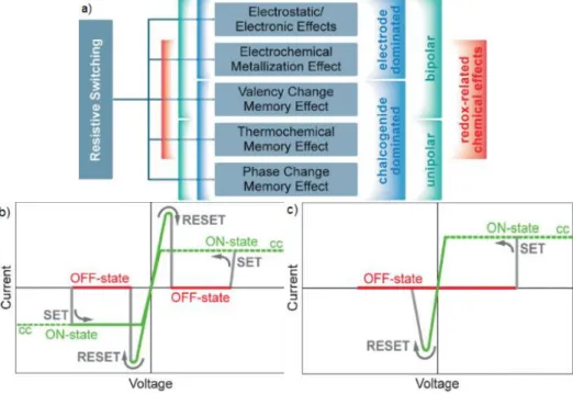
ReRAM[21] is a category of memory storage devices that includes every type of NVM (non volatile memory) devices based on the resistivity change of a given material. As such, there are several types of NVM that fall into this category, as illustrated in figure 1.1 a), and they are designated by the physical phenomena that leads to the resistive switching effect. Although all of these memory effects are electrically induced, the actual physical driving force behind the resistance switching mechanism is different for the different ReRAM types. For instance, phase change memory (PCM)[22][23] is characterized by the switching of the insulating material from a crystalline more conductive phase (on state), to an amorphous less conductive phase (off state) by voltage application; thermochemical memory (TCM)[24] effect can be described by the resistivity change of an insulating material due to chemical changes inside the material caused by temperature, which can be electrically induced by joule heating; valence change memory (VCM) and electrochemical memory (ECM) effect rely on redox reactions in the material (anions in the case of VCM and metal cations on the case of ECM) to alter the resistivity between electrodes[8].
Depending on whether it is the insulator or one of the metal electrodes that plays the dominant role towards the resistive switching effect, these devices can be split into two subcategories: electrode dominated, or insulator dominated. Insulator dominated ReRAM can include PCM, VCM and TCM, whereas ECM belong to the electrode dominated category.
Concerning the programming point of view, all ReRAM devices fall into two subcategories: unipolar or bipolar. Unipolar operation is defined by using voltage pulses independent of the polarity for the set and reset functions. In this case, the set voltage is always higher than the reset voltage, and the reset current is always higher than the set current because it is limited by compliance. Bipolar switching is characterized by performing the set operation in one polarity, and the reset operation in the opposite polarity. Typical I-V operation is shown in Figure 2.1 b) for unipolar behavior and c) for bipolar behavior.
Conductive bridging RAM devices inspired on solid-state
biopolymer electrolytes 4
2.2. CBRAM fundamentals and applications
CBRAM devices are a type of ReRAM devices characterized by switching its resistivity through the ECM effect. Plainly put, CBRAM are normally constituted by an electrode dominated, asymmetric MIM structure, composed by: an inert electrode (IE), an electrolyte and an electrochemically active electrode (AE) (e.g. copper (Cu) or silver (Ag)). Due to the asymmetry of the device structure, by application of a positive voltage bias on the AE, while grounding the IE, the oxidation of the active metal is provoked and an electric field between the two electrodes is generated along the electrolyte.
V
E
d
(2.1)Equation (2.1) describes the electric field (E) as a function of the voltage (V) and distance (d). In many cases, inorganic nanoparticles are dispersed in the electrolytic medium in an effort to charge the dispersed nanoparticles, reducing the effective electric field distance, and therefore reducing the working voltages [34].
The metal cations migrate along the electric field towards the grounded IE, when reaching this electrode, the cations are reduced and crystallized on the surface of the IE. By this process, eventually, a crystallized metallic filament will be formed between the two electrodes, short circuiting them, and changing the resistivity state between the electrodes. Equation (2.2) and (2.3) represent the anodic dissolution of a metal (M) to the ionic form, and the reduction and electrocrystallization of M, respectively:
z
M
M
e
(2.2)
-z
M
ze
M
(2.3)Since the behavior described depends on the oxidation of an electrode to achieve a high current state (HCS) and it depends on the reduction of a metallic filament to achieve the low current state (LCS), then the programming of CBRAM devices are characterized by bipolar operation (from hereon in, all current states will be mentioned as LCS and HCS). The setting operation requires a positive voltage bias to be applied on the AE to induce the formation of the filament, and the reset operation is performed at a negative polarity to reduce and break the metallic filament. Figure 2.2 shows a sketch of the operation of a typical CBRAM device comprised of an electrolyte sandwiched between a Ag AE and a platinum (Pt) IE.
Figure 2.2 – Sketch of the steps ((A) – (D)) of a set operation and a reset operation (E) on a typical CBRAM device [7]
Conductive bridging RAM devices inspired on solid-state
biopolymer electrolytes 5
Chalcogenide based materials are regarded as the most used and studied materials for CBRAM devices because of their well-known diffusion mechanisms towards copper (Cu2+) and silver (Ag+) ions. However, integration with CMOS technology in chalcogenide materials might be a problem. Oxides offer a great integration with CMOS technology, however CBRAM devices based on these materials typically operate at much lower currents and speeds, as well as suffering from high device-to-device and cycle-to-cycle uniformity problems, limiting their real application. Bilayer materials aim to improve oxide based materials uniformity and other performance problems by adding a diffusion layer to the oxide layer in order to better control the diffusion of the AE. Jana et al.[9] provided an extensive overview of the current state of the art on these three types of materials, and Waser et al.[7] extensively reviews the theory behind these switching mechanisms.
Regarding the latter category of materials applied in CBRAMs, an insight into biopolymer electrolytes and their application in electronics will be given in the following chapters.
2.3. Biopolymers: from fundamentals towards electronic applications
Biopolymers are natural occurring polymers originating from living organisms, often with a very well defined structure when compared to their synthetic counterparts. Due to their structure and origin, biopolymers possess very interesting characteristics, such as: biocompatibility, biodegradability, self-sustainability, thermal stability, low cost and solution processability at room temperature[26]. This set of properties made biopolymers to be established over time as an important resource for important economic sectors such as: packaging, food, medicine, paper and textile industries[27]. Most recently, due to the concern for the stagnation of the silicon based electronics industry, biopolymers are starting to gain relevance as an innovative material towards low cost printed and paper electronics[28]
Among various existing biopolymers, two stand out for being the most renewable and abundant on earth: cellulose and chitin. Cellulose mainly originates from plant cell walls, but can also be found on some sea organisms, fungi and bacteria. Its structure consists of a straight chain linkage of D-glucose units through mainly β(1→4) glycosidic bonds (some forms may possess α(1→4) glycosidic bonds). Chitin is the second most abundant biopolymer on Earth, after cellulose, and in contrast to cellulose, it is mainly extracted from fungi cell walls and the exoskeletons of crustaceans and insects. It is constituted by N-acetylglucosamine units linked by β(1→4) covalent bonds; plainly put, chitins structure can be comparable to that of cellulose, but with one hydroxyl group from each monomer substituted by an acetyl amine group.
For the purpose of solution processability, cellulose cannot be dissolved in common solvents due to the strong hydrogen bonds[29]. Cellulose dissolution has to be conducted, therefore, in other complex solvent systems, such as: lithium chloride/N,N-dimethylacetamide (LiCl/DMAc), N-methylmorpholine-N-oxide monohydrate (NMMO) and ionic liquids[30]. However these dissolution systems suffer from high cost, toxicity and volatility, limiting their applications. Alternatively, by substituting cellulose’s hydroxyl groups by other functional groups, cellulose derivatives that are soluble in ordinary solvents can be created. Examples of cellulose derivatives include: ethyl cellulose (EC), hydroxypropyl cellulose (HPC), methyl cellulose (MC) and carboxymethyl cellulose (CMC)[31]. Particularly, HPC results from the hydroxypropylation of cellulose, substituting some of the hydroxyl groups from the repeating glucose units of the cellulose backbone to hydroxypropyl groups, making it soluble in water and other common organic solvents[32].
Chitin, similarly to cellulose, cannot be dissolved in common solvents, as such, chitosan emerges as a derivative of chitin that is soluble in slightly acidic solutions, being the most used solvent system acetic acid aqueous solutions[33]. Chitosan derives from the deacetylation of chitin, therefore, its structure is comprised of N-glucosamine units linked through β(1→4) covalent bonds much like chitin. Figure 1.3 illustrates the chemical structure of cellulose, chitin and chitosan.
Figure 2.3 – Chemical structures of cellulose (a), chitin (b) and chitosan (c).
Most recently, the strive towards self-sustainable, low cost, green electronics has driven forward the research regarding biopolymer materials in electronics. The most notable role of biopolymer materials in electronics is as a free standing substrate material, and as a dielectric or electrolyte material,
Conductive bridging RAM devices inspired on solid-state
biopolymer electrolytes 6
due to its high capacitance, in a variety of systems including: batteries[34], [35], capacitors[36]–[39],thin film transistors (TFT)[40]–[46], and ReRAM devices[12]–[20].
Focusing on the latter application, Hosseini and Lee have reported the usage of AgNP-chitosan composite as a solid polymer electrolyte in CBRAM devices[16]. In their work, resistive switching is achieved in a MIM structure comprised of a Pt IE, AgNP-chitosan as a solid polymer electrolyte (SPE), and a Ag AE, either on a silicon (Si) substrate or a flexible polyethersulfone (PES) plastic substrate. These devices exhibited low voltage operation (±0.8V) a high On/Off ratio (Ion/Ioff) (105), high data retention (104 s), and an endurance of 100 program/erase (P/E) cycles. The same authors went on to develop similar devices while changing both contacts to magnesium (Mg)[13].
Most recently, Hosseini and Lee have developed ReRAM devices using starch and a starch-chitosan blend on a PET/ITO substrate that also serves as one electrode, while the other electrode is gold (Au)[18]. The fact that both electrodes are inert, make this an electrolyte dominated device. The authors postulate that the resistive switching comes from the formation of carbon rich filaments (CRF) provenient from the SPE, induced by joule heating.
Another work of interest is that of Nagashima et al[19], where cellulose nanofiber paper(CNP) is
functionalized with AgNP’s, acting as a SPE for the purpose of building a CBRAM device. In this work,
both a Pt/AgNP-CNP/Pt and a Pt/Ag-CNP/Ag architectures are explored, as well as the influence of the device area in the LCS. Both the Pt/AgNP-CNP/Pt and Pt/Ag-CNP/Ag structure show resistive switching, being that the latter, showed much greater switching behavior in terms of lower forming voltages, switching probability and retention (Annex A – C).
Other work regarding the usage of biopolymer in resistive switching memory devices include: a DNA biopolymer nanocomposite[15], silk[14] and AuNP’s in silk[20], sericin[17] and albumen[12]. Table 2.1 provides a summarized overview of some existing ReRAM technology using biopolymers.
Table 2.1 – Overview of existing ReRAM technology using biopolymers
SPE BE TE WORM Voltage(V) IOn/IOff Retention(s)
P/E endurance
(cycles)
Ref
AgNP-Chitosan Pt Ag No ±0.8 105 104 100 [16]
AgNP-Chitosan Mg Mg No [-3, 2] 102 104 60 [13]
Starch-Chitosan ITO Au No [-4, 2] 103 104 — [18]
AgNP-CNP Pt Ag or Pt No ±0.5 106 105 100 [19]
DNA
composite ITO Ag Yes ±6 102 105 — [15]
Silk ITO Al No ±15 10 103 120 [14]
AuNP-silk ITO Al No ±2 104 103 10 [20]
Sericin Au Ag No [-1.5, 3] 106 103 21 [17]
Albumen ITO Al No [-3, 4] 103 104 500 [12]
The fact that resistive switching phenomena (similar to CBRAM) has already been reported in biopolymer materials utilizing structures were both electrodes are inert, supports the possibility that CBRAM devices based on biopolymers could in fact possess a mixed switching mechanism consisting of thermochemical, valence change and electrochemical metallization effects.
As already demonstrated by Nagashima et al[19], cellulose can in fact be used as a solid polymer electrolyte towards resistive memory applications, although producing very interesting results, the solution processability of this CNP remains challenging.
Conductive bridging RAM devices inspired on solid-state
biopolymer electrolytes 7
3. MATERIALS AND METHODS
This chapter will focus on the steps that were taken in the fabrication and characterization process of the aforementioned devices. First, the AgNP-chitosan composite solution formulation will be presented. Then all the necessary steps towards device fabrication, and finally, how the characterization of the insulating material and electrical characterization of the devices were performed.
3.1. Materials and reagents
Low molecular weight chitosan powder (deacetylation degree: 75%-85%, CAS:9012-76-4), silver nitrate powder (AgNO3 ≥99.0%, CAS:7761-88-8) and acetic acid (CH3CO2H ≥ 99%, CAS:64-19-7) were purchased from Sigma-Aldrich, and hydroxypropyl cellulose powder (Mw ~ 100000, CAS:9004-64-2) was purchased from Acros organics.
3.2. AgNP-chitosan solution formulation
The procedure for the formulation of the AgNP-chitosan composite solution was adapted from [47].
Acetic acid was diluted to obtain a 1% (v/v) aqueous solution, chitosan flakes were then added in a 3% (w/v) and dissolved under vigorous stirring at ambient temperature overnight. 50mL of the prepared chitosan solution were then heated in an oil bath, under reflux, up to 95ºC under vigorous stirring (1100rpm), then, 20mL of a previously prepared AgNO3 aqueous solution with a certain concentration (7mM, 12mM, 26mM, 52mM) were added dropwise (this process results in a diluted 2.1% (w/v) chitosan solution). The mixture was kept under temperature and agitation for a total of 7h, while solution samples were taken hour by hour to evaluate the effect of the reaction time on the concentration of nanoparticles dispersed in the solution.
3.3. Device fabrication
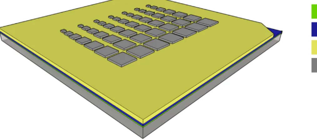
All fabricated devices used the same basic architecture: Glass/Ti/Pt/electrolyte/Ag. Figure 3.1 represents a basic schematic representation of the fabricated CBRAM devices.
Figure 3.1 – Schematic representation of the fabricated CBRAM devices
For the common bottom contact, a 20nm Ti adhesion layer and a 100nm Pt layer were deposited by e-beam evaporation.
The electrolyte material is comprised of either chitosan, HPC or the AgNP-chitosan composite deposited by spin coating. In order to achieve different thicknesses of the electrolyte layer, different solution concentrations of chitosan and HPC were used (1% (w/v), 2.1% (w/v), 3% (w/v) for chitosan, and 5%wt, 6%wt, 8%wt, and 10%wt for HPC) while maintaining the spin coating parameters for all solutions.
The spin coating process was performed as follows:
First, the Pt covered glass substrate was subjected to a 30min UV-ozone treatment in order to increase its hydrophilicity.
Ti
Pt
Electrolyte
Conductive bridging RAM devices inspired on solid-state
biopolymer electrolytes 8
Then, the solution is dispensed on the static substrate while being filtered through a 0.45µm syringe filter (the 3% (w/v) chitosan and 10%wt HPC solutions were filtered through a 0.8µm filter instead due to their higher viscosity).
A two-step spin coating process is performed by spinning the substrate at 1000rpm during 35s and then at 3000 rpm during 15s.
The substrate is then heated on a hotplate at 60ºC during 2min to evaporate any remaining solvents.
The Ag top electrodes were then deposited through e-beam evaporation with a thickness of 100nm and were patterned by shadow mask lithography. The Ag contacts pattern consists of a 7x7 matrix comprised of square contacts, where the area of the square contacts is varied from column to column as illustrated in figure 3.1. The studied areas were: 0.5mm2, 0.75 mm2, 1mm2, 1.25mm2, 1.5 mm2, 1.75mm2 and 2mm2.
Furthermore, the usage of Ag electrodes deposited through screen printing was also investigated. To this purpose, a Ag conductive ink (PE-AG-530 Flexible Silver Conductive ink) purchased from conductive compounds was passed through a patterned mesh (using the same pattern described above) followed by a 130ºC cure during 90 s on a hotplate. The used mesh has the following characteristics: mesh model 120; mesh count, 305 mesh/inch; aperture, 45µm; thread diameter, 34 µm; opening, 30.5%; screen thickness, 52-57µm. The usage of screen printed Ag electrodes were tested on the intermediate concentrations for both chitosan (2% (w/v)) and HPC (8%wt) electrolytes.
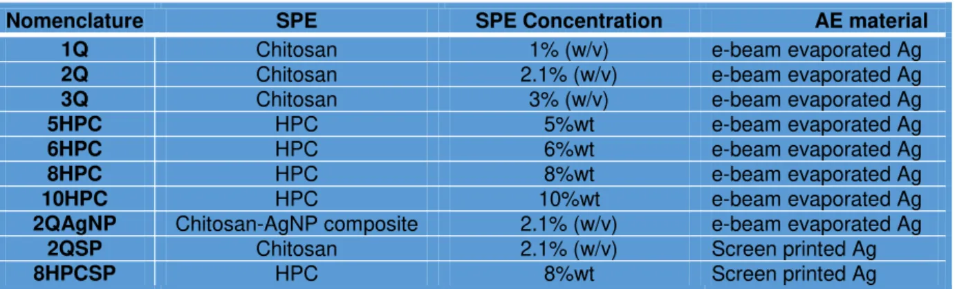
In this work, several devices were tested in order to study the influence of the electrolyte material, electrolyte thickness and the AE material in their electrical performance. Table 3.1 resumes the fabricated devices characteristics and their nomenclature from here on out.
Table 3.1 – Nomenclature and description of all fabricated devices
Nomenclature SPE SPE Concentration AE material
1Q Chitosan 1% (w/v) e-beam evaporated Ag
2Q Chitosan 2.1% (w/v) e-beam evaporated Ag
3Q Chitosan 3% (w/v) e-beam evaporated Ag
5HPC HPC 5%wt e-beam evaporated Ag
6HPC HPC 6%wt e-beam evaporated Ag
8HPC HPC 8%wt e-beam evaporated Ag
10HPC HPC 10%wt e-beam evaporated Ag
2QAgNP Chitosan-AgNP composite 2.1% (w/v) e-beam evaporated Ag
2QSP Chitosan 2.1% (w/v) Screen printed Ag
8HPCSP HPC 8%wt Screen printed Ag
3.4. Characterization
In order to evaluate the formation of AgNP in the chitosan solutions, UV-Vis spectrophotometry was performed using a PerkinElmer Lambda 950 UV-Vis-NIR spectrophotometer with a 2D detector module in absorption mode, using a wavelength range of 250 nm to 650 nm.
Thickness evaluation of the deposited films was performed by profilometer step measurements using an Ambios XP-Plus 200 Stylus Profilometer with the following parameters: speed = 0.1 mm/s, length = 0.5 mm, range = 100 µm, stylus force = 0.1 mg.
The morphology and composition of the chitosan-AgNP composite membrane was analyzed by scanning electron microscopy (SEM) and energy dispersive spectroscopy (EDS) using a Carl Zeiss Auriga crossbeam (SEM-FIB) workstation instrument equipped with an Oxford X-Ray energy dispersive spectrometer.
Conductive bridging RAM devices inspired on solid-state
biopolymer electrolytes 9
4. Results and discussion
4.1. UV-Visible absorption spectra
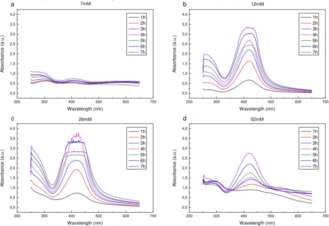
In order to evaluate the formation of stable AgNP’s in the composite solution, UV-visible absorption spectra was conducted on the solutions containing different silver loadings (7mM, 12mM, 26mM, 52mM), as well as evaluating the effect of the reaction time (1h-7h).
Figure 4.1 – UV-visible absorption spectra of the tested AgNP-chitosan solutions (7mM (a), 12mM (b), 26mM (c), 52mM (d)).
These results can be considered as a comparative study to evaluate the effect of the AgNO3 concentration and reaction time in the medium. All solutions present a maximum peak on the 400 – 420nm, wavelength range, indicating the presence of metallic AgNP’s.
The 7mM solution show a much lower absorption spectra compared to the more concentrated solutions. The 26mM and 52mM solutions show a higher full width at medium height (FWHM) than the 12mM solution, hinting that there is a higher dispersion in nanoparticles sizes in the medium. Therefore the preferred solution is the 12mM solution, for showing high absorption intensity at 420nm and having the lower FWHM.
Regarding the reaction time in the 12mM solution, a peak saturation can be observed for reaction times over 5h, therefore, the 4h reaction time is considered to be the optimum reaction time.
Taking these results into consideration, the 12mM solution at a 4h reaction time was selected to be used as the electrolyte layer in future experiments.
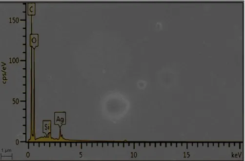
4.2. SEM-EDS analysis
To evaluate the morphological structure of the chitosan-AgNP composite membranes, SEM topographical imaging was carried out, and EDS was performed to analyze the composition of the membrane. Figure 4.2 shows the obtained SEM image of the composite membrane as well as the corresponding EDS analysis.
200 300 400 500 600 700
0,0 0,5 1,0 1,5 2,0 2,5 3,0 3,5 4,0
200 300 400 500 600 700
0,0 0,5 1,0 1,5 2,0 2,5 3,0 3,5 4,0
200 300 400 500 600 700
0,0 0,5 1,0 1,5 2,0 2,5 3,0 3,5 4,0
200 300 400 500 600 700
Conductive bridging RAM devices inspired on solid-state
biopolymer electrolytes 10
Figure 4.2 – Topographical view of the AgNP membrane obtained by SEM and the corresponding EDS analysis
Even though, there is no distinguishable dispersion of AgNP visible on the obtained SEM image, EDS analysis reveals a silver approximate concentration of 8.8wt%. This result supports the possibility that, even though not being clearly visible on a topographical view, AgNPs can in fact be well dispersed within the chitosan matrix.
4.3. Profilometer analysis
In order to test the effect of different SPE thicknesses in the electrical performance of the devices, various SPE’s using the same materials but different concentrations were used, while maintaining the spin coating parameters. This procedure was adopted mainly because, the film thickness dependence over the spin coating parameters such as time and spin speed are not linear (Annex D), therefore it is very challenging to achieve an intermediate film thickness by this method. By varying the solution concentration instead of the spinning parameters, a more linear relation can be obtained.
The profilometer measurements were performed by measuring the thickness of the electrolyte layer on five different sites, the average and the associated error were then calculated and are shown in Table 4.1.
Table 4.1 – Measured SPE thicknesses obtained for the different devices
Substrate Thickness (nm)
1Q 71,4 ± 10
2Q 304 ± 22
3Q 508,4 ± 91
5HPC 362,6 ± 7
6HPC 583 ± 19
8HPC 1135,2 ± 13
10HPC 1815,6 ± 10
2QAgNP 151 ± 11
2QSP 317 ± 8
8HPCSP 1 089 ± 37
Conductive bridging RAM devices inspired on solid-state
biopolymer electrolytes 11
4.4. Electrical analysis
4.4.1. Typical I-V characteristics
Since the electrical characteristics can vary greatly from device to device in the same substrate, all the electrical characteristics in the different substrates were evaluated. As such, a statistical study was conducted, in order to determine the effect of SPE thickness in the electrical performance.
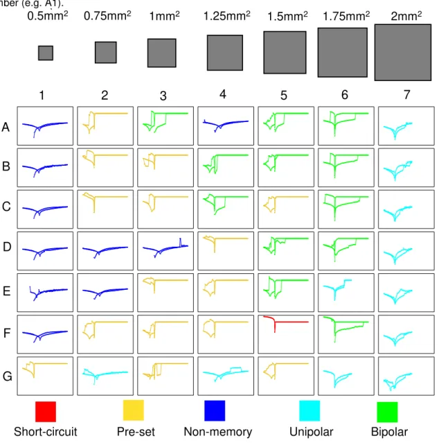
Figure 4.3 maps the I-V characteristics of all of the devices in the 2Q substrate according to their physical coordinates. The remaining maps can be found from Annex H – M. The rows have been labeled from A – G, and the columns from 1 – 7. Also, the devices electrode area are indicated below each column. From here on in, the device coordinates will be called by their row letter and their column number (e.g. A1).
Figure 4.3 – I-V Characteristics of all the devices on the 2Q substrate
By analyzing Figure 4.3, different switching behaviors can be observed along the substrate. For the purpose of this work, these different behaviors can be divided into five categories: non-memory, short circuit, pre-set, unipolar switching and bipolar switching.
Non-memory devices can be designated by simply demonstrating an insulating behavior and no resistive switching (e.g. A1, B1, etc.). These devices might show some small hysteretic behavior because of trapped oxygen vacancies in the electrolyte due to its elevated water content. To note, that even appearing as not working, there is a possibility that they might show resistive switching under different electrical programming. Figure 4.4 shows the behavior of the B1 device on the 2Q substrate, as a standard example of a non-memory device.
1
2
3
4
5
6
7
A
B
C
D
E
F
G
Short-circuit
Pre-set
Non-memory
Unipolar
Bipolar
2mm
21.75mm
21.5mm
21.25mm
21mm
20.75mm
2Conductive bridging RAM devices inspired on solid-state
biopolymer electrolytes 12
Figure 4.4 – I-V characteristics of the B1 device on the 2Q substrate, a typical example of a non-memory
Short circuited devices appear solely as a short circuit, not being able to ever be reset (e.g. F5). The appearance of these devices are most likely explained by defects of the electrolyte layer, or incomplete film coverage, allowing the deposited AE to be in direct contact with the bottom IE. Figure 4.5 shows the I-V curve of the F5 device, a typical example of a short circuited device.
Figure 4.5 – I-V characteristics of the F5 device on the 2Q substrate. A typical example of a short circuited device.
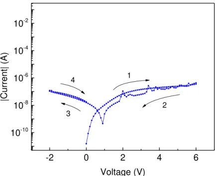
Pre-set devices are characterized by initially appearing in a HCS but being able to be reset by applying a negative voltage bias (e.g.E4, F4). Figure 4.6 illustrates the I-V characteristics of the C5 device on the 2Q substrate, a typical example of a pre-set device.
-2
0
2
4
6
10
-1010
-810
-610
-410
-2|Current| (A)
Voltage (V)
1
2 3
4
-2
0
2
4
6
10
-1010
-810
-610
-410
-2|Current| (A)
Conductive bridging RAM devices inspired on solid-state
biopolymer electrolytes 13
Figure 4.6 – I-V characteristics of the C5 device on the 2Q. A typical example of a pre-set device.
As represented in Figure 4.6, the reset of these devices might show a negative differential resistance (NDR). This means that the reset process is not performed instantaneously, but it rather achieves decreasing current levels until it reaches the final LCS. Under a certain programming, the NDR effect can be utilized towards the programming of multi-level cell’s (MLC), meaning that one device
might show multiple bit’s per cell. Even though this effect is apparent in these devices, the programming
of MLC in this case is uncontrollable.
One possible explanation towards the appearance of pre-set devices, is that silver diffuses into the electrolyte matrix when the contacts are deposited through e-beam evaporation[48], then it is possible to rupture the diffused filament through voltage application.
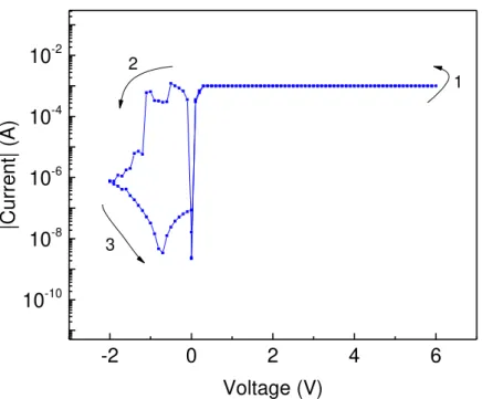
Unipolar switching devices as already described in chapter 2.1, exhibit resistive switching behavior independent of the voltage polarity applied. This behavior is most frequent in electrolyte dominated switching mechanisms such as TCM. Figure 4.7 shows the behavior of the G4 device on the 2Q substrate which is a typical example of unipolar operation.
Figure 4.7 – I-V characteristics of the G4 device. A typical example of unipolar operation.
In the figure above, a clear switching to a HCS is visible in (1), the current then drops back to the LCS by applying a higher voltage on the same polarity. This behavior is typical in unipolar operation. It
-2
0
2
4
6
10
-1010
-810
-610
-410
-2|Current| (A)
Voltage (V)
1 2
3
-2
0
2
4
6
10
-1010
-810
-610
-410
-2|Current| (A)
Voltage (V)
1
2
Conductive bridging RAM devices inspired on solid-state
biopolymer electrolytes 14
should be noted that, even though some devices shown in Figure 4.3 do switch to the HCS but do not drop back to the LCS by application of a higher voltage (e.g. D7, E7), we still consider them to exhibit unipolar operation, but the applied voltage simply was not sufficient to switch the device back to the LCS. These considerations are made for two reasons: the HCS does not match the CC, and when the reset operation begins, the device appears in the LCS.
Bipolar switching devices, as described in chapter 2.1 show resistive switching dependent of the voltage polarity. In this case, the devices appear to set at the positive voltage polarity, and reset when a negative voltage bias is applied, as is common for CBRAM devices.
Figure 4.8 – I-V characteristics of the C4 device on the 2Q substrate.A typical example of a bipolar switching device
As illustrated above, a clear switching to the HCS is performed in (1), it should be noted that the HCS must be limited by the CC to prevent the irreversible damaging of the device. The device exhibits a clear window in (2), then at a negative voltage bias, the device switches back to the LCS in (3). Much like the pre-set devices, this devices might exhibit NDR operation in the reset process.
Concerning the device electrode area dependency, by analyzing Figure 4.3, Vset seems to lower by decreasing the AE area, hinting that the switching mechanism responsible for the resistive switching might not solely be an ECM effect, since this effect is area independent, but it is possible that the switching mechanism is a mixture of the ECM effect with an electrolyte dependent effect such as TCM or VCM, mostly due to the presence of oxygen vacancies inside the electrolyte layer. Even though Vset seems to lower with the decreasing electrode area, since all of the devices are on the same substrate, other effects such as film uniformity issues can cause a great variability in device to device uniformity. We suggest that a new type of substrate should be fabricated were all of the patterned devices have the same size, in order to verify if the Vset is consistent in a larger sample group.
-2
0
2
4
6
10
-1010
-810
-610
-410
-2|Current| (A)
Voltage (V)
1 2 3
Conductive bridging RAM devices inspired on solid-state
biopolymer electrolytes 15
4.4.2. Thickness dependency on the electrical performance
Table 4.2 resumes the number of devices that belong to each of the categories mentioned above for the different produced substrates.
Table 4.2 – Device count by category in the different substrates
Substrate Non-memory Short-circuits Pre-set Unipolar Bipolar
1Q 0 47 2 0 0
2Q 10 1 15 11 12
3Q 8 16 14 5 6
2QAgNP 3 17 9 6 14
5HPC 0 35 12 0 2
6HPC
8
19 15 0 78HPC 32 5 5 2 5
10HPC 24 2 3 15 5
Even though a clear distinction cannot be made in terms of the I-V characteristics of the individual bipolar switching devices in each of the fabricated substrates, by analyzing Table 4.2, it is clear that the thickness of the electrolyte layer plays a very important role in terms of the yields obtained for each of the fabricated substrates.
As expected, it is observable that the number of short-circuits increases dramatically on the substrates with the lower electrolyte thicknesses (1Q and 5HPC). This is explainable by two theories: (1), silver diffusion during the AE deposition process irreversibly short-circuits the devices, or (2), the electric fields at which the devices are subjected in the initial forming process are too high, creating thick filaments that cannot be ruptured. The increase in the number of pre-set devices on the 5HPC substrate, supports (1).
Conductive bridging RAM devices inspired on solid-state
biopolymer electrolytes 16
4.4.3. Effect of the electrolyte material on the electrical performance.
In order to study how the electrical performance of the devices change with the different used materials, a small statistical study was conducted on the intermediate thickness devices (2Q and 8HPC) as well as the chitosan-AgNP composite device (2QAgNP).
For that purpose, and taking into consideration equation (2.1), the electric field at which the devices switch their current state was calculated for each of the measured bipolar devices (the reset values of the pre-set devices were taken into account as well), taking into account the measured SPE thickness for each of the substrates. Taking those values into account, the probability of encountering one device with a specific forming electric field in the respective substrate is as follows:
Figure 4.9 – Statistical analysis of the switching probability on the 2Q (left), 2QAgNP (middle) and 8HPC (right) devices
By analyzing the figure above, there is no clear improvement on the usage of the chitosan-AgNP electrolyte instead of a simple chitosan layer. It would be expected that the necessary electric field to set the device would be significantly lower in the AgNP composite, however, the applied electric fields to set and reset the 2Q and 2QAgNP devices are similar. Even though no improvement is clear in this
experiment, it is possible that the concentration of AgNP’s used was too low to have any effect on the
resistive switching of the devices. Further study, using higher concentrations of AgNP’s, would be
needed to understand the role that AgNP’s could have on the resistive switching of these devices.
The 8HPC substrate, shows electrical switching at similar voltage values than the chitosan devices, however, because the SPE films possess a thickness that is about 1 order higher than the chitosan films, the calculated electric field at which the electrical switching occurs is about 1 order lower than the chitosan films. One possibility that could explain the better functioning of HPC at higher thickness values than chitosan is that the defect density in HPC would be much higher than in the chitosan layers, therefore, the thickness of the HPC films need to be higher, in order to not short circuit the device beforehand.
4.4.4. Retention characteristics
In this chapter, results regarding the typical retention characteristics will be presented for devices in the 2Q, 2QSP, 6HPC and 10HPC substrates. Further testing on the other substrates was not possible due to time constraints.
Since it was already shown that device behavior varies greatly from device to device in the same substrate, different programming methods were used in the different measurements in order to obtain the retention results.
The 2Q device was programmed by applying a Vset = 1.5 V pulse, during tset = 2.5 s, with a CC = 500 µA. The HCS was measured by applying a constant Vread = 0.2 V bias during 30 h with no CC and measuring the devices current response. The reset was then performed by applying a Vreset = -3 V
-0.1 0.0 0.1 0.2 0 20 40 60 80 100
-0.1 0.0 0.1 0.2 -0.02 -0.01 0.00 0.01 0.02
Switching probability (%)
Set Reset
2Q
Electric field (MV/cm)
Conductive bridging RAM devices inspired on solid-state
biopolymer electrolytes 17
pulse during treset = 2.7 s with no CC. The LCS was then measured using the same programming as for the HCS. Figure 4.10 shows the results obtained.
Figure 4.10 – Tipical retention characteristics of the 2Q devices
As illustrated in Figure 4.10, the 2Q device showed remarkable retention characteristics, showing stable data retention times (tretention) of over 105 s with a IOn/Off≈ 102.
The 2QSP device was programmed as follows: a 0 V to 6.1 V I-V sweep with a CC = 500 µA was performed to set the device, the HCS was then measured during 30 h by applying a constant Vread = 0.2 V with no CC. The device was then reset by applying a Vreset = -3 V during treset = 2 s, with no CC, then the LCS was measured using the same programming as the HCS.
Figure 4.11 – Typical retention characteristics of the 2QSP devices. The inset shows the I-V curve of the initial forming step of the device
The 2QSP device showed retention of one stable HCS with an approximate current value of 4.6 mA during a tretention ≈ 6x10⁴ s, after that, the device seems to switch to a second HCS with an approximate current value of 0.5 µA. The LCS seems to decrease over time, by showing a current variance (ΔI) of approximately 103. Because of the variance of the LCS, the I
On/Off varies from 107 to 109 in the first HCS, and in the second HCS, IOn/Off≈ 105.
The 10HPC device was set by using a Vset = 1.5 V pulse over tset = 2.5 s, with a CC = 5 µA. The current response was then measured by applying a Vread = 0.2 V pulse with a CC of 1 µA from 10 to 10 min in an effort to avoid stressing the device.
10
210
310
410
510
-510
-410
-3 HCS LCSCurrent (A)
Time (s)
Read @ 0.2V~102
10
210
310
410
510
-1110
-910
-710
-510
-310
-110
110
310
5Curre
nt
(A)
Time (s)
HCS LCSRead @ 0.2V
~107
~105 ~109
0 1 2 3 4 5 6 10-11
Conductive bridging RAM devices inspired on solid-state
biopolymer electrolytes 18
Figure 4.12 – Typical retention characteristics for the 10HPC devices. Inset shows a short retention measurement of both the HCS (red) and LCS (blue)
The tested 10HPC device showed stable HCS = 1 µA retention during a tretention = 40 min, after which, the current drops to a LCS ≈ 0.02 µA. The inset of Figure 4.12. shows the read current state after a set operation and the current state after a reset operation, demonstrating that the known LCS of the device is comparable to the current state that the device presents for tretention > 40 min. It is probable that this device could show higher retention times if subjected to different programming.
By reducing the thickness of the electrolyte layer, more percolation paths are created between the two electrodes, leading to a better retention of the HCS. Consequently, the lower thickness leads to the stressing of the device on the LCS by application of the read voltage. Figure 4.13 shows the typical retention behavior of a 6HPC device under Vread = 0.2 V.
Figure 4.13 – Typical retention characteristics of the 6HPC devices under Vread = 0.2 V The HCS was able to be maintained up to 104 s, however, the LCS started to increase its current level at tretention≈ 2x10³ s.
The retention of the LCS can be improved by reducing the used Vread. Figure 4.14 – shows the typical retention characteristics of the 6HPC device under Vread = 0.1 V.
0
20
40
60
80
100
120
10
-810
-710
-6Current (A)
Time (min)
Read @ 0.2V~103 0.0 0.5 1.0 1.5 2.0 2.5 10-9
10-8 10-7
10-6 HCS
LCS C u rr e n t (A ) Time (s)
10
210
310
410
-810
-710
-610
-510
-410
-310
-2Current (A)
Time (s)
HCS
LCS
Read @ 0.2V
Conductive bridging RAM devices inspired on solid-state
biopolymer electrolytes 19
Figure 4.14 – Typical retention characteristics of the 6HPC device under a Vread = 0.1 V
At Vread = 0.1 V, it was possible to maintain the HCS, while improving the retention of the LCS up to tretention≈ 2x10⁴ s, at which point the LCS turns to the HCS
4.4.5. Endurance characteristics
In this chapter, the typical endurance characteristics for the devices in the following substrates will be presented: 2Q, 10HPC, 2QSP, and 8HPCSP. These tests are made in order to evaluate the devices ability to endure several P/E cycles.
For this purpose, 100 I-V cycles were performed on a 2Q device:
Figure 4.15 – 100 I-V cycles performed on the 2Q device.
It can be observed that the tested device shows rather low endurance, with only around three successful P/E cycles. One explanation for this low endurance is that, by subjecting the device to such high currents for a long period of time, the device switches from a bipolar switching behavior to a unipolar switching behavior. This is further supported by analyzing cycle number 48, which shows a typical unipolar behavior:
10
210
310
410
510
-1110
-910
-710
-510
-3Current (A)
Time (s)
HCS
LCS
Read @ 0.1V
10
6-2
-1
0
1
2
3
4
5
6
Conductive bridging RAM devices inspired on solid-state
biopolymer electrolytes 20
Figure 4.16 – I-V characteristics of the 2Q device at cycle number 48.
This type of behavior could be prevented, by using a different kind of programming. As such, the subsequent testing was performed using timed voltage pulses instead of I-V sweeps in order to reduce the stressing of the devices.
The tests consist on subjecting the selected devices to 100 P/E cycles using timed pulses with certain parameters (Vset, tset, Vreset, treset and CC) defined for each of the tested devices, and reading the current response of the device with a Vread = 0.2 V timed pulse after each set/reset pulse.
The setting parameters for each of the tested devices is presented in Table 4.3:
Table 4.3 – P/E endurance tests programming parameters for the tested devices
Substrate Vset
(V) tset (s) Vreset (V) treset (s) CCset (A) CCreset (A)
HCS CCread
(A)
LCS CCread
(A) 2Q 1.5 2 -3 2 2x10⁻⁶ 5x10⁻² 5x10⁻⁷ 5x10⁻⁷ 10HPC 1.5 2 -3 2 5x10⁻⁶ 5x10⁻² 10-6 10-6
2QSP 3 2 -3 1 5x10⁻⁴ 10-1 10-1 5x10⁻⁴ 8HPCSP 1.5 5 -4 5 10-3 10-1 10-3 10-3
It should be noted that the P/E endurance cycles were performed using Keithley 4200-SCS semiconductor measurement units (SMU) which enable the application of voltage bias for a long period of time (>1s), but offer very low precision in terms of the voltage pulse application times, in contrast to the pulse measurement units (PMU), which offer a very high precision in voltage pulse application times, but can only be used for fast pulses (≤1s). Therefore, the programmed times might differ greatly from the real voltage pulse application times.
-2
-1
0
1
2
3
4
5
6
Conductive bridging RAM devices inspired on solid-state
biopolymer electrolytes 21
Figure 4.17 – Typical endurance characteristics of the 2Q devices
This device shows two distinct current states with IOn/Off≈ 5. The presence of intermediate current states between HCS and LCS indicate the presence of an uncontrollable MLC behavior. Furthermore some measurements of the HCS appear on the LCS. One explanation for both of these behaviors is that the device exhibits some Vset dispersion (this is a well-known effect for CBRAM devices [9]), and the Vset or tset used is not sufficient to set the device at some specific cycles. Another possibility is that after an undetermined number of cycles, the device will start to behave as a unipolar memory, and the set voltage pulse cannot switch the device to the HCS. However, a HCS is still observable at cycle number 100, indicating that the device can exhibit resistive switching for 100 cycles but due to incorrect programming, the device can fail to set at randomly distributed cycles.
Figure 4.18 – Typical endurance characteristics for the 10HPC devices
The endurance characteristics of the 10HPC device shows similar behavior to that described for the 2Q, however, the LCS shows a current value of 10-8, showing IOn/Off≈ 102. The lower current value of the LCS could be attributed to the higher thickness of the HPC devices when compared to the chitosan devices as shown in Table 4.1. Much like the 2Q device, there are some intermediate current states, indicating an uncontrollable MLC behavior, as well as randomly distributed set failures.
0
20
40
60
80
100
10
-810
-710
-6 HCSLCS
Current (A)
Cycle
Read @ 0.2V0
20
40
60
80
100
10
-1010
-910
-810
-710
-6HCS LCS
Current (A)
Conductive bridging RAM devices inspired on solid-state
biopolymer electrolytes 22
Figure 4.19 – Typical endurance characteristics of the 2QSP device. The inset shows a close up of cycles 60 to 70, demonstranting that a smaller memory window is present
The 2QSP device clearly shows uncontrollable MLC behavior, since there is no well-defined HCS in the initial P/E cycles. There seems, however, to be a tendency for the HCS to decrease, this could be caused by some stressing of the device by the reset voltage pulse. Since the CC does not limit the reset voltage pulse, but limits the set voltage pulse, the filaments within the electrolyte could become iteratively thinner with each cycle, causing the HCS to decrease over time. This issue could possibly be resolved by increasing CCset or tset.
At around cycle number 59, even though the memory window seems to decrease considerably, there seems to be two well defined current states with a IOn/Off≈ 2. Similar to the previously shown devices, this device might still randomly set, indicating that it might still be working after the endurance test, however, the used programming was not ideal.
Figure 4.20 – Typical endurance characteristics of the 8HPCSP device
The 8HPCSP device initially shows two stable current states with a IOn/Off≈ 107. Similar to the other presented devices, an uncontrollable MLC behavior is observable by the presence of intermediate current states. At cycle number 46, the device seems to consistently fail the setting procedure. Endurance behavior could be improved by using faster but higher reset pulses.
Endurance characteristics reveal that all tested devices endure multiple P/E cycles. We suggest that most of the failing P/E cycles might be a result of inappropriate programming rather than device
0
20
40
60
80
100
10
-910
-710
-510
-310
-110
1 HCS LCSCurrent (A)
Cycle
Read @ 0.2V60 62 64 66 68 70 1x10⁻⁷ 2x10⁻⁷ 3x10⁻⁷ C u rr e n t (A ) Cycle
![Figure 2.2 – Sketch of the steps ((A) – (D)) of a set operation and a reset operation (E) on a typical CBRAM device [7]](https://thumb-eu.123doks.com/thumbv2/123dok_br/16692382.743692/24.892.257.678.633.1001/figure-sketch-steps-operation-operation-typical-cbram-device.webp)