Joana Rita Marques de Sousa Almeida
Bachelor in Micro and Nanotechnologies Engineering
Fabrication and Functionalization
of In
2O
3Thin Film Transistors for
Biosensing Applications
Dissertation submitted in partial fulfillment of the requirements for the degree of Masters in Micro and Nanotechnologies
Engineering
April, 2017
Adviser:
Jaakko Leppäniemi, Senior Scientist, VTT Technical
Research Centre of Finland Ltd
Fabrication and Functionalization of In2O3 Thin Film Transistors for Biosensing Applications
Copyright © Joana Rita Marques de Sousa Almeida, Faculdade de Ciências e Tecnologia, Universidade Nova de Lisboa, 2017.
“Here’s to strong women. May we know them. May we be them. May we raise them.”
Acknowledgements
First of all, I would like to give thanks to everybody in the team of Printed Sensors and Electronic Devices of VTT who made me feel welcome since day one and were always available to help me, even with the smallest things, making working at VTT so smooth and enjoyable. A very special thanks to my supervisor Jaakko Leppäniemi without whom this dissertation would not be possible at all! Thanks for all the patience and hard work! A special thanks to Dr. Maria Smolander, team leader, for such a warm welcome in her team, for making this incredible opportunity available for me and for her kindness. Thank you!
Agradeço também à Professora Dr. Elvira Fortunato, minha orientadora nesta dissertação, e a todos os docentes da FCT-UNL que fizeram com que a participação neste projeto europeu, BET-EU, fosse possível. Foi uma experiência única e extremamente enriquecedora tanto a nível profissional como pessoal. Queria também agradecer em especial ao Professor Luís Pereira, por dar-me a conhecer esta oportunidade e por toda a sua ajuda em torná-la possível. Obrigada!
Nada disto seria possível sem as pessoas a quem devo tudo, os meus pais. Obrigada por me apoiarem em todas as decisões e desafios, mesmo quando um deles é “ir fazer a tese para o Ártico”. E por serem os melhores exemplos que poderia seguir. Obrigada por tudo! Agora só falta o curso de cinema e prometo que não vos meto num lar... Queria também agradecer e dedicar esta tese aos meus avós, porque ter uma neta engenheira é bonito, mesmo que seja de um curso muito manhoso...
Aos amigos de sempre, obrigada por me aceitarem quando perdi o sotaque do Norte, quando de vez em quando pedia uma imperial, quando vos chamei “putos”, quando deixei de ver os jogos do FCP e sobretudo por me perdoarem a traição de ir estudar para Marrocos. Imperdoável. Obrigada por continuarem lá a cada fim de semana que ia a casa, pelas visitas surpresas a Lisboa e noites de magia no Bairro Alto. Sara, Rebeca, Maria, Marta, vocês sabem! Agora é rumo às Grandiosas 2017!!
Aos amigos para sempre, obrigada. Obrigada por me mostrarem que o Sul nem é assim tão mau. Por fazerem valer a pena estar a mais de 300 km de casa, mesmo quando a avaliação contínua teimava em provar o contrário. Obrigada por me ajudarem a formar a pessoa que sou hoje (para o bem e para o mal! A culpa também é vossa). Obrigada por tornarem estes últimos anos memoráveis, com histórias e momentos que nos manterão ligados para sempre. A todos os migos e migas, especialmente Constança (Concha), Mariana, Trofas (meu Fredo), Jacinto, Jaime, Pena, restante família basolhense, aos meus lindos e incríveis afilhados, aos migos da 202 e a toda a gente que durante estes 5 anos me pagou uma cerveja: Obrigada, foram o melhor que a faculdade me deu e o que me fez ficar quando questionava todas as decisões da minha vida! MICRO & NANO 11/12!
Abstract
Due to unprecedented interest in the development of new ways of detection, quantification and monitoring of different molecules and compounds, the biosensor arises as the most promising approach to fulfil such requirements [1]. The biosensor is a device which can detect and quantify the presence of certain chemical compounds or biological reactions by the use of electrical, thermal or optical signals. Combining this with the advantages of microelectronic technologies, such as well developed miniaturization and ability to amplify and control an input, biosensors based on TFTs are currently the most studied devices for this kind of applications [2].
The goal of this dissertation was to fabricate In2O3-based TFTs functionalized with
3-aminopropyltriethoxysilane (APTES) to work as pH sensors. For that several concepts were used: using Al electrodes and an insulator layer, SU-8; and using Cr/Au electrodes with two different designs, planar and interdigitated. The devices with best performance were the ones with Cr/Au electrodes and planar configuration. The functionalization and liquid-gating of these devices are successfully demonstrated in this work. However, a cleaning method had to be established in order to measure the same sample several times. The APTES film showed poor stability to the cleaning method performed. This poor stability can be due to siloxane bond hydrolysis catalyzed by the amine group which could also cause uncontrolled polymerization/oglimerization of the amine groups [3]. Both will lead to a decrease in the device’s performance. The measurement procedure and/or the cleaning method of the sample will have to be optimized in the future.
Resumo
Devido a um interesse sem precedentes no desenvolvimento de novas formas de deteção, quantificação e monotorização de diferentes moléculas e compostos, o biossensor surge como a abordagem mais promissora para alcançar tais requerimentos [1]. O biossensor é um dispositivo capaz de detetar e quantificar a presença de certos compostos químicos ou reações biológicas através do uso de sinais elétricos, térmicos ou óticos. Combinando vantagens da microeletrónica, como a miniaturização, já bem estabelecida, e a capacidade de amplificar e controlar um input, biossensores com base em TFTs são atualmente o dispositivo mais estudado para este tipo de aplicações [2].
O objetivo desta dissertação foi fabricar TFTs de In2O3 funcionalizados com
Table of Contents
ACKNOWLEDGEMENTS II
ABSTRACT IV
RESUMO VI
TABLE OF CONTENTS VIII
LIST OF FIGURES X
LIST OF TABLES XI
ACRONYMS XIII
SYMBOLS XV
OBJECTIVE XVIII
WORK STRUCTURE XVIII
CHAPTER 1 1
INTRODUCTION 1
1.1TFT AS A BIOSENSOR 2
1.1.1OPERATIONAL PRINCIPLE OF TFTS 2
1.2LIQUID GATING TFTS –ISFETS 5
1.3CHEMICAL FUNCTIONALIZATION -APTES 7
CHAPTER 2 11
MATERIALS AND METHODS 11
2.1LAYOUTS CONCEPTS 11
2.2SI-CHIPS:CLEANING PROCESS 12
2.3INKJET PRINTING:IN2O3AND SU-8 LAYERS 12
2.3.1IN2O3:INK SYNTHESIS AND PRINTING 13
2.3.2SU-8 PRINTING OPTIMIZATION 14
2.4THERMAL EVAPORATION:AL AND CR/AU 14
2.5APTES FUNCTIONALIZATION 15
2.6PHSOLUTIONS 15
2.7CHARACTERIZATION TECHNIQUES: 16
2.7.1ELECTRICAL CHARACTERIZATION 16 2.7.2OPTICAL MICROSCOPE,FTIR,AFM AND SEM 16
CHAPTER 3 19
RESULTS AND DISCUSSION 19
3.1PART ONE:SU-8 PASSIVATED DEVICES WITH AL ELECTRODES 19 3.2PART TWO:UNPASSIVATED DEVICES WITH CR/AL ELECTRODES - PLANAR VS INTERDIGITATED DESIGNS 22 3.3PART THREE:APTES DEPOSITION AND OPTIMIZATION OF LIQUID GATED DEVICES 24
CHAPTER 4 33
CONCLUSION &FUTURE PERSPECTIVES 33
REFERENCES 35
APPENDICES 39
1.LAYOUTS AUTOCAD 39
List of Figures
FIGURE 1:SCHEMATIC DIAGRAM OF TFT STRUTURE USING SI DOPED P++ SUBSTRATE AS BACK GATE. ... 3
FIGURE 2:SCHEMATIC DIAGRAM OF ISFET STRUTURE USED. ... 6
FIGURE 3: A) CHEMICAL STRUCTUTURE OF APTES MOLECULE [3]; B) SILANIZATION REACTION BETWEEN APTES AND THE HYDROXYLATED SURFACE ORIGINATING TO A APTES FUNCTIONALIZED SURFACE.THE TERMINAL AMINE GROUPS ALLOW FURTHER FUNCTIONALIZATION (ADAPTED FROM [16]); AND C) THE PH-SENSING MECHANISM OCCURS BY PROTONATION OF IN2O3 SURFACE HYDROXYL GROUPS AND PRIMARY AMINES OF APTES AT DECREASING PH(INCREASING PROTON CONCENTRATION)[4]. ... 7
FIGURE 4:SCHEMATIC REPRESENTATION OF ADSORBED APTES ON A SILICON WAFER IN AN ANHYDROUS TOLUENE SOLUTION; A) ETHOXY GROUPS OF ADSORBED APTES ARE HYDROLYZED AND FORM SILOXANE BONDS WITH SURFACE SILANOLS (MONOLAYER STRUCTURE); AND B) FURTHER SILOXANE CONDENSATION BETWEEN APTES BOUND TO THE SURFACE AND DISSOLVED APTES AND/OR NONCOVALENT ADSORPTION OF DISSOLVED APTES(MULTILAYERS STRUCTURE)[15]. ... 8
FIGURE 5:DESIGN OF THE LAYOUTS USED.CONCEPT A) AND B): A SU-8 LAYER IS USED AS INSULATOR BETWEEN THE SOURCE AND DRAIN ELECTRODES AND A LOCAL AU GATE ELECTRODE; CONCEPT C) AND D): BASED ON THE SAME DESIGNS USED BY RIM ET AL.[4], WHERE A LOCAL GATING IS APPLIED, USING A PT WIRE. ... 11
FIGURE 6:DROP WATCHER IMAGE OF IN2O3 PRINTING OPTIMIZATION PROCESS. A) STROBE DELAY 20 µS; B) STROBE DELAY 40 µS; AND C) STROBE DELAY 100 µS. ... 13
FIGURE 7: A)1 LAYER OF SU-8 PRINTED AT 30ºC; B)2 LAYERS OF SU-8 PRINTED AT 30ºC; C)1 LAYER OF SU-8 PRINTED AT 50ºC; AND D)2LAYERS OF SU-8 PRINTED AT 50ºC. ... 19
FIGURE 8: A) SURFACE WITH 12S AR PLASMA TREATMENT; B) SURFACE WASHED WITH DIW/ACE/IPA; C)AL ELECTRODES WITH POST-ANNEALING; AND D)NO SURFACE TREATMENT. ... 20
FIGURE 9: A) TRANSFER CURVE OF TFT MEASURED BEFORE SU-8 SPIN-COATING AND AR PLASMA TREATMENT; B) TRANSFER CURVE OF TFT MEASURED AFTER AR PLASMA TREATMENT (12S) AND SU-8 SPIN-COATING WITH SUBSQUENT ANNEALLING PROCESS OF DEVICE (5 MIN AT 130ºC); AND C) TRANSFER CURVE OF TFT MEASURED AFTER SECOND ANNEALLING PROCESS OF DEVICE (2H AT 150ºC). ... 21
FIGURE 10:TRANSFER CURVES OF TFTS WITH DIFFERENT CR THICKNESSES:5NM,10NM AND 15 NM AND AU THICKNESS OF 45 NM ALONG WITH CALCULATED SATURATION MOBILITY (RIGHT AXIS) WITH W=1MM AND L=80 UM. ... 22
FIGURE 11: A)OPTICAL MICROSCOPE IMAGE OF INTERDIGITATED CONFIGURATION; B)OPTICAL MICROSCOPE IMAGE OF PLANAR CONFIGURATION; C)SEM IMAGE OF PLANAR CONFIGURATION; D)SEM IMAGE OF INTERDIGITATED CONFIGURATION; AND E)SEM IMAGE OF "SHADOW EFFECT" ON THE INTERDIGITATED CONFIGURATION. ... 23
FIGURE 12:TRANSFER CURVES OF TFTS WITH DIFFERENT DESIGNS AND RATIOS W/L: A) INTERDIGITADED WITH 10“FINGERS” (W/L=875); B) PLANAR WITH L=80µM AND W=2MM (W/L=25); C) PLANAR WITH L=160µM AND W=2MM (W/L=12,5); AND D) PLANAR WITH L=320µM AND W=2MM (W/L=6,25). ... 24
FIGURE 13: A)TRANSFER CURVE OF TFT OBTAINED BY LIQUID GATING USING PBS SOLUTION WITH PH=7,35(SEE TABLE 1); B) OUTPUT CURVE OF TFT USING PBS SOLUTION WITH PH=7,35. ... 25
FIGURE 14:DIAGRAM OF CLEANING METHODS USED BETWEEN MEASUREMENTS. ... 26
FIGURE 15: A) REPRESENTATIVE RESPONSE OF TFT TO DIFFERENT PBS SOLUTIONS WITH DIFFERENT PH LEVELS, USING A DIW RINSING OF THE SAMPLE BETWEEN MEASUREMENTS ; B) REPRESENTATIVE RESPONSE OF TFT TO DIFFERENT PBS SOLUTIONS WITH DIFFERENT PH LEVELS, USING DIW SONICATION FOR 30 MIN AT 60ºC BETWEEN MEASUREMENTS. 26 FIGURE 16:REPRESENTATIVE RESPONSE OF TFTA AND TFTB, EACH ONE MEASURED TWO TIMES WITH THE SAME PBS SOLUTION (PH=7,35) WITH DIW SONICATION FOR 30 MIN AT 60ºC BETWEEN MEASUREMENTS. ... 27
FIGURE 17: FTIR SPECTRA OF THE SAMPLES DESCRIBED ON TABLE 2, REPRESENTING DIFFERENT STAGES OF APTES FUNTIONALIZATION AND MEASUREMENT OF THE DEVICES. ... 28
FIGURE 18:SURFACE ROUGHNESS MEAUSURED BY AFM OF SAMPE 1. ... 29
FIGURE 19:SURFACE ROUGHNESS MEAUSURED BY AFM OF SAMPE 2. ... 29
FIGURE 20:SURFACE ROUGHNESS MEAUSURED BY AFM OF SAMPE 3. ... 29
FIGURE 21:SURFACE ROUGHNESS MEAUSURED BY AFM OF SAMPE 4. ... 30
FIGURE 22:MORPHOLOGY ANALYSIS WITH IMAGES OBTAINED BY SEM OF SAMPLE 4. ... 31
FIGURE 23:AUTOCAD DESIGNS OF EVAPORATION MAKS (RED), FOR METALLIC ELECTRODES AND SEMICONDUCTOR PATTERNS INKJET PRINTED (BLUE),IN2O3. ... 39
List of Tables
TABLE 1: PH TABLE OF THE DIFFERENT PBS SOLUTION SYNTHETIZED AS WELL WAS THE VOLUMES OF KH2PO4 AND NA2HPO4
Acronyms
ACE Acetone
AFM Atomic force microscope
APTES 3-Aminopropyltriethoxysilane
DIW Deionized water
DOD Drop on demand
DS Drop spacing
EDL Electrical double layer
FET Field effect transistor
FTIR Fourier transform infrared spectroscopy
IPA Isopropanol
ISFET Ion-sensitive field effect transistor
IUPAC International Union of Pure and Applied Chemistry
PBS Phosphate-buffered solution
SAM Self-assembled monolayer
SEM Scanning electron microscope
Symbols
Ci Gate capacitance per unit
gd Conductance
gm Transconductance
ID Drain current
IG Gate current
IS Source current
L Length of conductive channel
S Sub-threshold swing
VD Drain voltage
VG Gate voltage
VON Turn-on voltage
VS Source voltage
VT Threshold voltage
W Width of conductive channel
wt% Weight percentage
µ Mobility
µeff Effective mobility
µFE Field-effect mobility
Objective
This thesis aims to produce sensitive In2O3-based thin film transistors (TFTs)
functionalized with a self-assembled monolayer (SAM) of NH2 – terminated silanes to
work as pH sensors. The thin film transistor sensors developed in this work could be use as biosensors in future noninvasive, rapid and low-cost health monitoring platform [4].
Work Structure
Chapter 1
Introduction
We live in an exceptional time regarding the speed of technological advances. Just by looking to our world 20 or 30 years ago we can see the extraordinary changes in our day-to-day life. It is up to us, scientists, researchers, engineers, to make the most of this unprecedented time. One of the main objectives of scientific research has been improving the quality of life. And one of the most important fields of research work towards that goal is the biomedical field, more specifically health monitoring. Health monitoring can be an essential tool in elderly care, tracking of infectious diseases, early detection of diseases, sport-related applications, among others.
In recent years, many new ways of detection, quantification and monitoring of different biological and chemical compounds have been studied. Fast analysis, cheap production, portability, sensibility, versatility and good performance are the essential requirements for the development of these new kind of health monitoring devices, where the biosensor is one of the most promising approaches to fulfill these requirements [2].
There has been significant interest in developing pH sensors for very small amounts of fluids since the pH values of blood and interstitial fluid are considered important indicators of human health. The acid-base balance (concentration of H+) in the
extracellular fluid is tightly regulated and maintained by human buffer systems, lungs and kidneys, such that the pH of the arterial blood is maintained within a range between 7,37 and 7,42. This delicate balance is threatened continuously by additions of extra acids or bases to body fluids from either respiratory or metabolic processes [5].
Through the detection of different pH solutions, it’s possible to detect and quantify many other molecules, such as D-glucose, following the same detection principle [4]. The detection of such species represents a great advance for the functionalized TFT-based biosensors. This approach can then be applied to the detection and quantification of other molecules and compounds, therefore unveiling a brand new approach for the monitoring and early detection of countless diseases.
1.1 TFT as a Biosensor
According to the IUPAC definition, a biosensor is “a device which uses specific biochemical reactions mediated by isolated enzymes, immunosystems, tissues, organelles, or whole cells to detect chemical compounds, usually by use of electrical, thermal or optical signals”. This kind of devices contains two functional parts: a bioselective layer in direct contact with a physical transducer, which transforms the occurrence of a specific kind of biorecognition into an electrical or optical signal. The amplitude of this transformed signal will be directly correlated with the concentration of the analyzed compound – analyte. The fabrication of such devices involve the use of biologically active materials that can be divided in two main groups: catalytic (enzymes, cells, tissues) and noncatalytic or affinity (antibodies, acids). Currently the transducers used are: electrochemical, optical, calometric and acoustic [1].
Biosensors based on semiconductors structures, such as transistors, has been the most up-and-coming design receiving a lot of attention in the last decades due to the wide potential of microelectronics. Features like the well-developed miniaturization, integration into portable devices and the ability to amplify and control input signals are some of the main advantages for the use of the transistor technology in such applications [1, 2].
1.1.1
Operational Principle of TFTs
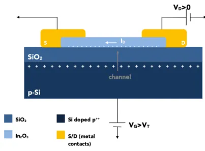
The thin film transistors (TFT) are devices consisting of three terminals (source, drain and gate). A thin semiconductor layer is placed between the source (S) and drain (D) electrodes on the same plane and a dielectric layer is located between the gate electrode and semiconductor, therefore vertically separating them.
The working principle of these devices relies on the control of the current flowing between the drain and source (ID) through the variation of the potential between the
gate and source electrodes (VG). This will prompt an injection of free carriers (electrons
Figure 1: Schematic diagram of TFT struture using Si doped p++ substrate as back gate.
Considering n-type TFTs, these can work in enhancement or depletion mode depending if the threshold voltage (VT) is positive or negative, respectively. VT
corresponds to the VG for which the accumulation layer or conductive channel is formed
in the channel region. Therefore, when VG>VT, a substantial density of electrons will be
accumulated in the interface dielectric/semiconductor and a large IDS will start flowing,
depending on the drain-to-source potential (VD). This state is designated by “on-state”
and involves two main regimes: linear/triode mode and saturation mode, depending on the VD value [7, 8]:
• If VD < VG – VT, the TFT is in linear/triode mode and ID is described by:
I"= C%µ'(W
L V,− V. V"− 1 2V
1
" (1) ,
where C% is the gate capacitance per unit area, µ'( is the field-effect mobility, W is the channel width, and L is the channel length of the device. For the linear regime with VD<<VG - VT, the quadratic term is usually neglected.
• If VD ≥ VG - VT, the TFT is in saturation mode and IDS is described by:
I"=1 2C%µ456
W
L V,− V.
1
(2) ,
where µ456 is the saturation mobility.
• The on/off ratio is defined by the ratio between the maximum to the minimum ID. The minimum ID can be given by the noise level of the measurement or by
the leakage current of the gate (IG), as for maximum ID depends on the
semiconductor material itself and on the efficiency of capacitive injection by the field-effect [8];
• VON corresponds to the VG at which ID starts to increase, that is the VG necessary
to fully turn-off the transistor.
• Subthreshold swing (S) indicates the minimum VG to increase ID by one decade.
Typically, S << 1, around 0,10-0,30 V dec:; and small values result in higher speeds and lower power consumption [8].
𝑆 =
𝜕𝑙𝑜𝑔(𝐼C)
𝜕𝑉F|𝑚𝑎𝑥
:;
(3)
• Mobility (µ) is related with the efficiency of carrier transportation in a material, thus affecting directly the maximum ID and switching speed of the device. It can
be affected by scattering mechanisms, such as lattice vibrations, ionized impurities, grain boundaries and other structural defects. The different mechanisms to extract the µ are described below [8]:
o Effective mobility (µKLL) is considered as the most correct estimation of µ. It is determined by the conductance (gd) at low VD.
µKLL = gN C%
W
L V,− V.
(4)
with gN = OPQ
ORQ;
o Field-effect mobility (µ'() is one of the most used methods to determine µ and it is obtained by the transconductance (gm) at low VD
[8].
:µ'(= gS C%
W
L V" (5)
with gS= OPQ
ORT;
µ456=
𝜕 I" 𝜕V,
1
1 2C%
W L
(6)
In this work, the semiconductor material is based on wide bandgap semiconducting metal oxides. The first reports of oxide-semiconductor TFTs showing good performance devices date to the early 2000’s. Initially, most of the research work was devoted to binary oxides such as ZnO, In2O3 and SnO2, but in 2003 Nomura et al. [10] reported the
use of InGaO3(ZnO)5 (GIZO) single-crystalline semiconductor layer in a TFT. By obtaining
impressive values for the effective mobility (80 cm2 V-1 s-1), turn-on voltage of -0,5V and
current on/off ratio of 106. This work proved that high-performance TFTs based on oxide
semiconductors are a reality. The developments since that have been focused on finding optimal materials and structures for oxide TFTs used in next-generation displays [8]. For the processing of such metal oxide TFT devices, solution processed techniques have received a lot of attention in recent years due to its properties. One example of this approach is the inkjet printing used in this work. This technique will bring advantages, such as, fast and simple prototyping, reduced material waste and ability coat uncommon substrates, among others [11].
1.2 Liquid Gating TFTs – ISFETs
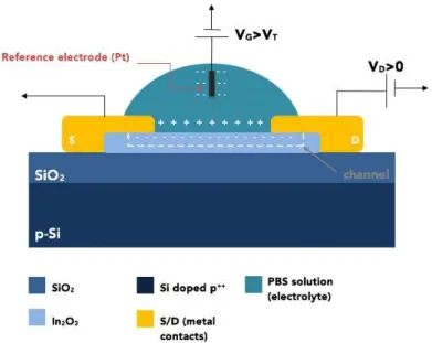
When using the TFT technology on biosensing applications there is a change in the classical structure of the device. In this case, the gate is replaced by a reference electrode. These types of devices are called ion-sensitive field-effect transistors (ISFETs).
The ISFET, is a FET device used for measuring ion concentrations in electrolyte solution. For example, in this work, when the ion concentration of H+ changes in pH
measurements, the current through the transistor will change accordingly. In a n-channel ISFET device, upon positive polarization of the gate, the anions of the electrolyte solution will migrate towards the vicinity of the reference electrode, while cations will be attracted toward the electrolyte-semiconductor interface, resulting in the formation of an electrical double layer (EDL) at both interfaces. The double layer acts as a dipole thus establishing an electrical field across the interface [2].
In the devices fabricated in this work, several phosphate-buffered saline (PBS) solutions, with different pH levels, were used as the gate electrode. The surface hydrolysis of indium hydroxide groups (In-OH) groups in the In2O3 surface varies with the PBS solution
used due to its pH value. This variation in the In2O3 charge is due to the addition or
donation of protons between the hydroxyl groups of the In2O3 and the electrolyte in the
semiconductor-electrolyte interface [12].
In this work, the semiconductor, In2O3, was functionalized with APTES. According to Rim
molecules, on the In2O3 layer. Thus the addition and donation of protons will occur
between the amine groups of the functionalized surface and the electrolyte. This reaction will be explained in more detail next.
The ISFET is a variant of the conventional TFT. Fig. 2 represents a schematic diagram of ISFET configuration used in the present work. The electrolyte is then in contact with the semiconductor which is sensitive to hydrogen ions. Thereby the VT is also sensitive to
interfacial potential at the electrolyte-semiconductor interface. Hence, any change in this interfacial potential, would result in a shift of the conductance of the semiconductor [2].
Figure 2: Schematic diagram of ISFET struture used.
In the specific case of the structure used in this work, illustrated on fig. 2, the electrolyte (PBS solution) and the reference electrode (Pt wire) will act as the gate electrode.
Therefore, when a positive potential is applied at the reference electrode, Pt wire, the ions of the electrolyte will move in such a way that the negative ions will be attracted to the vicinity of the Pt wire while the positive ions in the electrolyte will be repelled to the surface of the In2O3. This accumulation of positive ions on the In2O3 surface will attract
the electrons of the semiconductor forming a conductive channel at the top of the In2O3.
If instead a negative voltage is applied at the Pt wire, the device would have a similar behavior, only involving the symmetrical species of the ones mentioned before. In these devices the SiO2 and Si layers will only act as substrate, having no other role besides
supporting the device.
In addition to this action, with the functionalization of the semiconductor surface, the sensitivity of the current to H+ ions can be modified by the addition of APTES molecules
where the acidic conditions lead to protonation of the amine group and basic conditions to the deprotonation of the hydroxyl groups, as shown on fig. 3 c). These changes will contribute to the shift of VT, improving the devices sensibility.
can also be applied to these devices. Since in these devices the electric field is formed at the vicinity of the semiconductor in an EDL, it is difficult to calculate the Ci and
therefore, the saturation mobility for these devices was not calculated.
1.3
Chemical Functionalization - APTES
The ability to control surface functionalization is essential for several applications such as biosensors, as will be demonstrated in this dissertation. A more precise control over the surface functionalization will expand the functionality of the biosensors. Several organic molecules which can self-assemble and form monolayers can modify the intrinsic properties of the sensor surfaces, thus improving its ability to immobilize a specific molecule or protein [13].
A most common approach is to attach alkoxysilanes through the formation of Si-O-Si bonds between the silanol groups and the surface. 3-Aminopropyltriethoxysilane (APTES) is one the most used organosilanes in the process of silanization because the presence of its amine terminal group (–NH2) on the surface has a major importance in
biological applications. The presence of amine groups can catalyze, inter- or intra-molecularly, the reaction between silane molecules and surface silanol groups to form siloxane bonds [3]. The process of producing a self-assembled monolayer (SAM) of APTES on silicon surface is quite complex although the principle behind it is fairly simple [14].
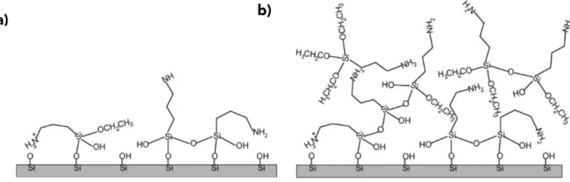
The process starts with the hydrolysis of ethoxy groups in APTES causing the formation of silanols. The presence of water at the surface is therefore required to catalyze the reaction since it is responsible for the first step of the process. Thus, control of the moisture during functionalization is crucial. These silanol groups formed from APTES will then condense with surface hydroxyl groups. This leads to the APTES monolayer
Figure 3: a) Chemical structuture of APTES molecule [3]; b) silanization reaction between APTES and the hydroxylated surface originating to a APTES functionalized surface. The terminal amine groups allow further functionalization (Adapted from [16]); and c) the pH-sensing
mechanism occurs by protonation of In2O3 surface hydroxyl groups and primary amines of
APTES at decreasing pH (increasing proton concentration) [4].
In2O3 on Si
substrate
In2O3 on Si
substrate
a) b)
via lateral siloxane network in which the amine groups are oriented away from the underlying silicon surface. This will allow them to react with the electrolyte as required for the successful performance of the biosensor [15]. However, as mentioned before, this process is far more complex and sensitive to many reaction conditions, such as reaction time, cleaning process of excess amount of APTES, amount of water present in the reaction, to name a few.
The complexity of the APTES silanization is essentially due to the presence of the amine group and its tendency to enter in conflicting reactions with other molecules, like the indium hydroxide groups present on the surface and/or in the neighboring hydrolyzed APTES via bonding or electrostatic interactions. These will bring two major problems:
§ will significantly reduce the amount of silanol groups available for further condensation as required for obtaining APTES film with the correct structure.
§ and will also promote polymerization of APTES through intermolecular condensation reactions, as can be seen on fig. 4 b), where amine groups react with silanol groups from the surface. These intermolecular reactions will produce multiple layers of APTES which are not suitable for this application, since the structure obtained this way has the amine groups of the surface superimposed by the polymerized APTES, as illustrated on fig. 4 b).
The polymerization of APTES can be horizontal and vertical. The first occurs when formed silanol groups interact with each other via condensation and form siloxane bonds. The vertical multilayering occurs when APTES molecules are physisorbed to each other when the surface is already APTES treated. This will lead to layers with amine groups oriented the wrong way for biosensing applications, as it can be seen on fig. 4 b) [14–16]. For this reason, it is fundamental to assure that the APTES film has sufficient amine groups with the required structure. It is possible to control crucial parameters such as adsorbed APTES and amount of layers deposited, by controlling the reaction conditions, such as solvent for APTES, the amount of water present in the system, the reaction time, among other. [13–15].
The conditions studied in this work, in order to obtain a APTES monolayer were mainly: time of the reaction (see appendix 2), the cleaning process of the excess amount of
a) b)
Chapter 2
Materials and Methods
2.1 Layouts Concepts
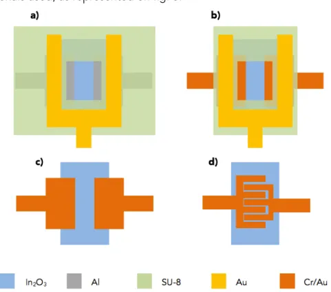
To a better understanding and optimization of the performance of the devices fabricated during this work, four different concepts of transistor layouts were considered. The concepts differ in the design of the electrodes, source and drain, and on the materials used, as represented on fig. 5.
Figure 5: Design of the layouts used. Concept a) and b): a SU-8 layer is used as insulator between the source and drain electrodes and a local Au gate electrode; concept c) and d): based on the same designs used by Rim et al. [4], where a local gating is applied, using a Pt wire.
The design of the evaporation masks for the electrodes and of the inkjet-printed layers, namely In2O3 and SU-8, were done using the software AutoCAD. Each design had
The semiconductor layer, In2O3, and insulator layer, SU-8, were both done by inkjet
printing. The purpose of the SU-8 in the devices with concepts a) and b) is to separate the source and drain electrodes from the Au top gate. In devices with concept a), the SU-8 insulator also protects the source and drain electrodes. Since in this concept, the metallic contacts are made from Al, it was necessary to add an insulator layer between the metallic contacts and the PBS solution (electrolyte) when performing the local gating, due to the fact that the Al oxidizes very easily. The SU-8 layer will then protect the Al contacts from the oxidation, while assuring a high carrier injection and preserving the good electrical properties of In2O3 TFTs.
It is possible to work around this problem by using an inert metal, such as the Cr/Au electrodes, where it is still possible to obtain TFTs with good performance and without any oxidation problem, as can be seen in concepts c) and d), of fig.5. In these concepts there is no need to use a protective layer on the source and drain electrodes or to separate them from a top gate contact, since with these concepts the local gating is performed using a Pt wire. The planar and interdigitated configuration were designed to verify which one would be more sensitive and how they would influence the performance of pH sensor.
2.2 Si-Chips: Cleaning process
In this project, p-type Si/SiO2 wafers (2012 E&M, Japan) were cutted in chips with the
following dimensions: 13,52 × 13,52 mm. The cleaning process of the chips starts with the removal of a photoresist layer, used to cover during the cutting. For that the sample are immersed in a bath of acetone (ACE) at 60ºC for 10 min. After the bath, the chips were rinsed with isopropanol (IPA) and dried with nitrogen (N2) gun (this step and all the
following rinses and dryings between baths were carried for a single chip at a time). Then the chips were immersed again in a bath of deionized water (DIW) for 15 min at 40ºC with sonication. After that they were rinsed with ACE and dried with N2. The third
immersion was done in ACE for 15 min at 40ºC and sonication and then they were rinsed with IPA and dried with N2. The last immersion was done in IPA for 15 min at 40ºC with
sonication. Finally, they were rinsed with IPA, dried with N2, and carefully stored.
2.3 Inkjet Printing: In
2O
3and SU-8 layers
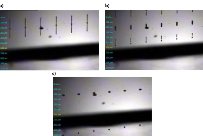
pulse that will eject the ink onto the substrate [11]. The process of optimization of the droplet is represented on fig. 6.
2.3.1 In
2O
3: Ink synthesis and printing
The semiconductor used in this work was indium oxide (In2O3). This choice was made
based on VTT’s experience with the printing of this material using the technique described before [18–20]. In2O3 is a n-type transparent semiconducting oxide. It shares
many properties with ZnO, SnO2, CdO and Ga2O3, and it is usually used in applications
such as in gas sensors or as transparent conducting oxide. These conventional applications typically suffice with a lower material quality thus allowing for inexpensive synthesis when compared to semiconductor standards in terms of crystallinity and purity. Only within the last decade, In2O3 and other semiconducting oxides have been
re-discovered as true wide bandgap semiconductors, requiring highest possible material quality and purity that has been the standard for established for other semiconductors. This approach opens perspectives for the use of In2O3 as active device
material in novel applications, such as in transparent electronics [21].
The ink preparation, VTT’s standard procedure was used, [18–20] , which will be briefly described next. The synthesis starts by preparing 0,2M concentration of indium nitrate (In(NO3)3) in 2-methoxyethanol (99,8% anhydrous from Sigma Aldrich). Two kinds of
In(NO3)3 were used in the work, for the first batch (ink 1) 99,9% In(NO3)3 from Sigma
Aldrich, while the second batch (ink 2-5) the In(NO3)3 99,9% from Epivalence Ltd. Then
the ink was shaked for 15 min at 250 rpm and after that mixed with a magnetic stirrer
a) b)
c)
Figure 6: Drop watcher image of In2O3 printing optimization process. a) strobe delay 20 µs; b) strobe delay
bar overnight in a water bath at 75ºC. Then a filtration step was done, using a 0.45 µm pore size PTFE filter in order to obtain a clear a transparent solution. Finally, 10 wt% of ethylene glycol (99,8% anhydrous from Sigma-Aldrich) was added to the filtered solution and mixed for 15 min at 250 rpm. According to Leppäniemi et al. [20], the
In-nitrate precursor should be well-converted to In2O3 when annealed at 300ºC and would
form a nanocrystalline structure with cubic In2O3.
Initially, the substrates were treated with O2 plasma for 1 min (≈200 W, Diener Nano) in
order to improve the wettability of the surface before printing of the semiconductor layer. The printing conditions, the following parameters were used: DS of 75 µm; nozzle angle of 17.2º; 10 nozzles; droplet in-flight between 5-7 m/s; frequency of 1kHz; trapezoidal waveform; jetting voltage between 16-20 V, which was then adjusted and optimized for each nozzle, see fig. 6. The number of layers printed were 2. After the printing the samples were dried at 90ºC on a hot plate for 15 min and then annealed at 300ºC for 30 min. For the first batches the drying and annealing steps were done in air and then for latter batches in a box with a controlled humidity (RH≈20-30%).
2.3.2 SU-8 printing optimization
The SU-8 used was a based epoxy resist from MicroChem. The goal of its usage was to combine the unique properties of SU-8, such as high chemical resistance, excellent thermal stability and low Young’s modulus, with the advantages of the inkjet printing techniques. For optimizing the printing of this layer several parameters were studied, such as design of the printing, cartridge angle, plate temperature and surface treatment in order to alter the surface energy of the substrate.
For the inkjet printing of the SU-8 layer the following parameters were used: DS of 55 µm; nozzle angle of 14º; 3 or 4 nozzles; trapezoidal waveform; jetting voltage of 17-19 V, which was then adjusted and optimized for each nozzle; and plate temperature of 30ºC or 50ºC. To optimize this process several parameters were studied, as will be demonstrating in the next chapter. These parameters were: number of SU-8 layers printed, plate temperature, and pre-treatments of Al surfaces, since in the final devices the SU-8 layer would be printed on top of the metallic electrodes.
2.4
Thermal Evaporation: Al and Cr/Au
The deposition of source and drain electrodes was done using thermal evaporation through a shadow mask. In a first phase of this work, we began by fabricating the devices of concept a), fig. 5, since it was a process already used by VTT, which led to TFTs with high mobility [18, 19]. Thus, the Al contacts were evaporated with thickness of ≈ 45 nm and after that the samples were post-annealed for 30 min at 150ºC.For the rest of the concepts b), c) and d) illustrated on fig. 5, the electrodes were evaporated using Cr and Au. Cr is used in order to improve the adhesion of Au to the In2O3 surface since Au has
bad adhesion to surfaces in general. The lower work function of Cr will result in a better match between the conduction band of the In2O3 semiconductor and the Fermi level of
The evaporations of both metallic layers were done in one evaporation run but at different times. It was necessary to study which would be the optimal amount of Cr. For this purpose, the TFT performance was studied for the following combinations: Cr≈ 5 nm, Au≈ 45nm; Cr≈ 10nm, Au≈ 45nm; Cr≈ 15nm, Au≈ 45nm.
2.5
APTES functionalization
For the functionalization of the devices for the pH sensing, a solution of 2 wt% APTES (99% from Sigma-Aldrich) in anhydrous toluene (99,8% from Sigma-Aldrich) was prepared. Then samples are immersed in the 2% APTES solution. The amount of time that the samples are immersed in the solution in order to create a APTES film on the In2O3 surface was one of the parameters studied, this will be discussed in the next
chapter. Another parameter, that we learn, is crucial for the success of the functionalization is the cleaning step, which is done after the immersion. The several cleaning processes studied are described and discussed in the next chapter.
2.6
pH Solutions
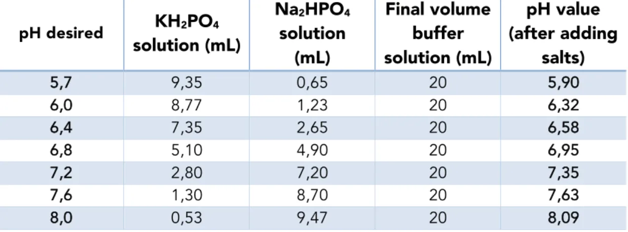
After having optimized the device fabrication process and having the working devices properly functionalized, the next phase was to proceeded to the liquid gating of the best working devices. For doing that, was necessary to previously prepare several PBS solutions with different pH values to then study the pH response of the sensor devices. For the synthesis of the PBS solutions used, were prepared 100 mL of 0,2 M of sodium phosphate dibasic (Na2HPO4) (≥98,5% from Sigma-Aldrich), by dissolving 5,362 g of
Na2HPO4 in 50 mL of H2O and then adjusting the final volume to 100 mL with H2O. After
that, 100 mL of 0,2 M of potassium phosphate monobasic (KH2PO4) (≥98,0% from
Sigma-Aldrich) was prepared, by dissolving 2,72 g of KH2PO4 in 50 mL of H2O and then
adjusting the final volume to 100 mL with H2O. Afterwards different volumes of each
solution were mixed, following the table 1 below, in order to obtain different pH values. Finally 160 mg of sodium chloride (NaCl) (≥99,5% from Sigma-Aldrich) and 4 mg of potassium chloride (KCl) (≥99,5% from Merck Millipore) were added to each of the buffer solutions. By adding these salts, the pH values will be slightly adjusted, therefore the pH of each of the solution was then measured. All the results are shown in table 1 below.
Table 1: pH table of the different PBS solution synthetized as well was the volumes of KH2PO4
and Na2HPO4 used.
pH desired
KH
2PO
4solution (mL)
Na
2HPO
4solution
(mL)
Final volume
buffer
solution (mL)
pH value
(after adding
salts)
5,7 9,35 0,65 20 5,90
6,0 8,77 1,23 20 6,32
6,4 7,35 2,65 20 6,58
6,8 5,10 4,90 20 6,95
7,2 2,80 7,20 20 7,35
7,6 1,30 8,70 20 7,63
2.7
Characterization Techniques:
2.7.1 Electrical Characterization
The TFT devices were electrically characterized using a semiconductor analyzer (Keithley 4200 SCS) and the measurements were conducted in a dark environment.
Initially, before any functionalization was performed, the devices were measured using the back gate (as represented on fig. 1) in order to select the best devices fabricated. After having selected the best ones, the process was continued for these with the functionalization and the liquid gating measurements (as represented on fig. 2). For the first measurements of the transfer and output curves of the TFTs using the back-gate (fig. 1) the standard Au probes were used, while for the liquid gating the reference electrode used was platinum (Pt) (fig. 2). This choice was based on the properties of the Pt, such as an inert metal, high stability to oxidation and has the right binding energy to H, for this kind of application [22].
For the back gating measurements, the p-Si substrate was used as the back gate. The transfer and output curve of the devices were then measured. For the transfer curve, back and forth curves were recorded in saturation mode by sweeping the gate voltage in 0,5V steps, with a range from VG=-10V to VG=20V and then back again to VG=-10V,
while keeping the drain voltage constant, VD = 20 V. For the output back and forth curves
were recorded by sweeping the drain voltage in 1V steps with a range from VD=-1V to
VD=20V and then back again to VD=-1V, while keeping the gate voltage constant. These
double sweeps of VD were carried for different values of VG, those being: 0V; 5V; 10V;
15V and 20V.
Finally, to study the sensor functionality of the final devices, a new set of measurements was done this time with the liquid gating instead of the back gating procedure. Therefore, to study the transfer curve of the devices, back and forth curves were recorded in saturation mode by sweeping the gate voltage in 0,05V steps, with a range from VG=-0,2V to VG=0,5V and then back again to VG=-0,2V, while keeping the drain
voltage constant VD = 0,2V. For the output: back and forth curves were recorded by
sweeping the drain voltage in 0,025V steps, with a range from VD=-0,025V to VD=0,025V
and then back again to VD=-0,025V, while keeping the gate voltage constant. These
double sweeps of VD were carried for different values of VG, those being: 0V; 0,1V; 0,2V;
0,4V and 0,5V.
2.7.2 Optical microscope, FTIR, AFM and SEM
Throughout this work was used an optical microscope, Olympus BX60 with Olympus SC30 digital camera in order to provide visual information about the quality of In2O3 and
SU-8 printing, as well as, the visual appearance of the evaporated metallic electrodes.
In order to perform a more thorough analysis of the samples, atomic force microscope (AFM) (Veeco Nanoscope 3) was used. This technique provided a better insight to surface roughness, thus making it possible to study the quality and uniformity of the layers.
Fourier transform infrared spectroscopy (FTIR), was performed with Ge-crystal in attenuated total reflection (ATR) mode at 4 cm-1 resolution (Thermo Scientific Nicolet
iS50) with a angle of 60ºC. This analysis was performed in order to do a qualitative study, to verify the presence of certain chemical bonds on the samples analyzed.
These two characterization techniques, AFM and FTIR, were used in the final phase, the APTES functionalization, to evaluate the sensor devices.
Chapter 3
Results and Discussion
3.1
Part One:
SU-8 passivated devices with Al electrodes
As already stated in this dissertation, this work was started with the production of devices following the configuration of concept a), represented on fig. 5, since the process of In2O3 based TFTs with Al contacts was already successfully established
procedure at VTT [19]. For this concept the SU-8 was crucial for protecting the Al from the electrolyte when performing the liquid gating.
The process started with the printing and optimization of the SU-8 layer. In this initial phase the printing of this material revealed to be rather complicated especially over time, due to the SU-8 polymers accumulating at the nozzle which leads to nozzle clogging as the solvent evaporates over time when the nozzle is idle. In order to solve this problem, an intense cleaning cycle was done between each printing passage.
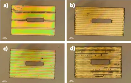
Even with a rigorous cleaning cycle the majority of the nozzles would stop working after a while, so the printings were done with only 3 to 4 working nozzles. The nozzle angle was also changed from the one that was indicated bythe printing software, from 12.5º to 14º. The drop spacing used was 55 µm, as indicated by the manufacture company. The nozzle angle was increased in order to avoid gaps between adjacent printings sweeps of the SU-8 layer that occur due to ink creeping. An example of these gaps is showed on fig. 7 a), between the first and second sweeps.
Optical microscope images in fig. 7 above, show the best results for the SU-8 layer under different printing conditions. The parameters that revealed to influence the most to the printing process were: plate temperature (at 30ºC and 50ºC) and number of layers printed (1 and 2 layers). Fig. 7 b) shows the best, thus the optimized conditions are 2 layers printed at 30ºC.
Having this initial part optimized, the next step was to the study the inkjet printing of SU-8 on top of Al electrodes, as that would be the actual configuration on the final devices. As anticipated the printing didn’t behave as it did on top of Si substrate, since the surface energy of the SiO2 is different than the surface energy of Al, which leads to
a different wetting behavior. As showed in fig. 7 a), when SU-8 is printed on top of Al surfaces there is the appearance of gaps between printing sweeps and the appearance of small holes. Therefore, a series of surface treatments were tested in order to improve the quality of the printing. Some of the results of these treatments are represented below on fig. 8.
Figure 8: a) surface with 12s Ar plasma treatment; b) surface washed with DIW/ACE/IPA; c) Al electrodes with post-annealing; and d) No surface treatment.
Three different kinds of surface treatments were done on top of the Al contacts before the inkjet printing of the SU-8:
• Treatment A: 12s argon (Ar) plasma treatment performed, in order to increase the surface energy of the Al surface and expect to improve the wetting of the ink on the surface, fig. 8 a);
• Treatment B: after the evaporation of Al contacts, the samples were rinsed again with acetone (ACE), isopropanol (IPA) and deionized water (DIW) in order to try to provide the Al electrodes with the same adsorbed molecules as the Si/SiO2
substrates have after the initial cleaning process, as described on Chapter 2, fig.8 b);
Fig. 8 shows the best results obtained for the different surface treatments. The best results were obtained with treatment A (Ar plasma), since with this treatment a uniform and well defined pattern was obtained with SU-8 on both top of SiO2 and Al surfaces,
as shown in fig. 8 a). All the other treatments presented some holes and discontinuities, especially in the borders between contacts and substrate, suggesting that the lack of quality of the printed SU-8 layer arises from the different surface energies of Al and SiO2.
Finally, was time to study the influence of Ar plasma on the performance of the devices to conclude if this treatment was a viable option. For these devices the In2O3
ink used was ink 1 and the SU-8 layer was spin-coated instead of inkjet printed due to the fact that the first method is more simple, less time consuming and suitable for this analysis since the main goal was to study how the surface treatment A and the SU-8 layer affected the performance of the In2O3 TFT devices, fig. 9. For devices fabricated
with Al electrodes the saturation mobility obtained was 3 cm2 V-1 s-1.
For studying the influence on the Ar plasma treatment on the devices, the electrical characterization was performed at different stages of the process. Initially, the device was measured before any plasma treatment, fig. 9 a). After having that transfer curve as reference, the samples were then submitted to Ar plasma for 12s and spin-coated with SU-8. Subsequently the samples were re-measured and the results showed that the devices have become too conductive. This effect of the Ar plasma treatment on the devices is mainly due to the changes on the charge carrier concentration that this treatment induces on the back channel of the TFT. This change on the carrier concentration happens because Ar plasma will deplete the semiconductor In2O3 from
oxygen, creating oxygen vacancies and promoting the formation of OH groups at the top surface that can act as charge donors [18]. In order to try to restore the good results obtained before, the samples were annealed under different conditions. The first annealing process was done for 5 min at 130ºC in a hot plate, as suggested by the manufacturer specifications for SU-8, and measured right after. As showed on fig. 9 b), the first baking did not improve the device’s performance, therefore a second annealing process was done for 2h at 150ºC to hard bake the SU-8. The results were improved, as
b)
c)
)
a)
showed in fig.9 c), but it’s still far from the initial results. Even though it is possible to observe gate modulation and distinguish a “kink” there is no “off-state”. The reason for the improvement on the performance of the device with the subsequent annealing process it is still unknown but many theories have been established. One of these reasons is suggested by Fortunato et al. [8], in which it is speculated that the annealing process will cause cross-linking of the SU-8 polymer leaving H+ ions available (due to the
decomposition of the photoacid generator present in SU-8) close to the interface between the insulator and semiconductor which, somehow, will help re-establish a depletion layer close to the top surface of the semiconductor.
Given the non-optimal, depletion-type performance of the TFT devices obtained using the concept a), due to the surface treatments required for the SU-8 printing, other concepts were studied where there is no demand for an insulator layer in the initial liquid-gate testing phase.
3.2
Part Two:
Unpassivated devices with Cr/Al electrodes -
planar vs interdigitated designs
The concepts c) and d) shown in fig. 5 were both a solution to the problems obtained previously. Au is an inert metal therefore there is no need to use SU-8 as a protective for the initial liquid-gating testing phase. The first step was to optimize the thickness of these layers. As explained before on Chapter 2, the use of Cr has merely the role to improve the adhesion of the Au layer to the surface, otherwise the Au would be the only metal used in the electrodes. Thus was necessary to optimize the thickness of Cr used in order to obtain the best performance possible. Three different thicknesses of Cr were studied: 5 nm, 10 nm and 15 nm; while maintaining the Au thickness constant at 45 nm. In all the following devices the inks used for In2O3 printing were inks 2 to 5.
From the results obtained, the Cr thickness with the best performance was 10 nm. Fig. 10 shows the best results obtained for the saturation mobility for each thickness.
Devices using a Cr contact layer with 10 nm and a Au layer with 45 nm achieved a saturation mobility value of approximately 0,62 cm2 V-1 s-1.
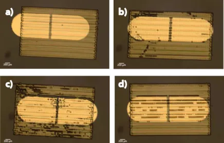
The next step was choosing which design concept, planar or interdigitated, would achieve better performance as TFTs. After the evaporation and measurements of several interdigitated devices the results showed that these were too conductive. Some of these devices were submitted to a post annealing in order to limit the charge carrier concentration [19, 20]. The problem of too high conductivity was enhanced by the “shadow affect” prevailing in these samples, as showed on fig 11 e). This “shadow effect” is more severe in this kind of configuration due to its small features. Although the evaporation of both metals is done at once, for the first evaporation the Cr is placed in the center of the evaporator chamber while the Au is place in the left extreme of the evaporator. This difference in the materials positioning is the most prominent reason for this “shadow effect”. Other contribution for this effect is the fact that in the evaporation mask the interdigitated design is placed in a corner of the mask. Thus these samples are further way from the center of the mask where the evaporated thickness should be more equal. For the planar configuration this effect is not so severe.
a)
b)
c)
d)
e)
The best electrical results obtained for each design evaporated are represented on fig. 12. The designs in study were: interdigitated with 10 “fingers”; and different combinations for the ratio W/L of the planar electrodes, those being L=80µm/W=2mm, L=160µm/W=2mm and L=320µm/W=2mm.
As represented on fig. 12 a), b), c) and d), the best performance is achieved with the planar design, more specifically with L= 160 µm, the saturation mobility achieved was approximately 1,5 cm2 V-1 s-1. This result is most likely a coincidence since within the
same sample all devices presented a substantial variation for saturation mobility. Still, it is safe to conclude that the planar configuration of the electrodes presents a better option especially due to the poor reproducibility of the interdigitated configuration.
3.3
Part Three:
APTES deposition and optimization of liquid
gated devices
The functionalization of the In2O3 semiconductor layer of the devices has several
parameters to be considered, such as the reaction time and cleaning method after deposition for removing the excess amount of the APTES.
c)
a)
d)
b)
Initially, to test the liquid gating of the devices, the APTES functionalization was done by immersing the TFTs in the prepared solution of 2wt% APTES in anhydrous toluene for 30 min. Samples were immediately rinsed with toluene for approximately 1min, fig. 13.
Figure 13: a) Transfer curve of TFT obtained by liquid gating using PBS solution with pH=7,35 (see table 1); b) Output curve of TFT using PBS solution with pH=7,35.
The first results obtained demonstrate the successful performance of APTES-treated and liquid-gated devices with low operation voltage. These show a stable performance with expected behavior, as represented in fig. 13. The measurements represented above on fig. 13 were performed using a PBS solution with pH=7,35 (see table 1).
Although, after a few consecutive measurements the performance deteriorated. Hence, the deposition conditions had to be improved (see appendix 2). According to Rim et al. and Joonyeong et al. [4, 15],in order to do that the reaction time had to be decreased and the sample had to be submitted to a more intensive cleaning with toluene in order to remove the excess of APTES for obtaining a sufficient amount of amine groups with the required structure, as explained previously on Chapter 1 (Section 1.3). After some tests involving several immersion times and cleaning procedures with toluene, the following conditions were defined: immersion for 10 min in the 2wt% APTES in anhydrous toluene followed by sonication in toluene for 10 min at room temperature.
The pH sensor response of the devices was then measured using PBS solutions with different concentrations, hence different pH levels, see table 1. Since there was not an automatic mechanism available to increase and/or decrease the concentration of the solutions on the device over time, it was necessary establish a cleaning method for the samples between measurements. This cleaning method was necessary because the measurements were carried in a dark box exposed to room conditions, thus after a few minutes the droplet of PBS would dry and leave salts in the device surface which would affect the results obtained in the next measurement.
Below, fig. 14 shows a diagram with the steps taken in order to improve the cleaning method of the samples between measurements is shown.
Figure 14: Diagram of cleaning methods used between measurements.
Figure 15: a) representative response of TFT to different PBS solutions with different pH levels, using a DIW rinsing of the sample between measurements ; b) representative response of TFT to different PBS solutions with different pH levels, using DIW sonication for 30 min at 60ºC between measurements.
The measurements were carried for 3 different pH levels (pH=8,09; pH=7,35; pH=5,90). The order of the measurements was from highest to lowest concentration: pH=5,90; pH=7,35 and pH=8,09. This order was used to assure that the cleaning method was working properly, since for a higher concentration of the solution in study a larger amount of salts would be left on the sample and that way the efficiency of the cleaning method would be properly analyzed. The devices subjected o the rigorous cleaning with DIW sonication at 60ºC for 30 min had the expected performance as represented on fig. 15 b). For pH=5,09 the ID response was the highest, given that this solution had
the highest concentrations of H+ ions; for pH=8,09 the I
D response was the lowest, given
that this solution had the lowest concentrations of H+ ions; and pH= 7,35 had I D
response in between the previous values. Rinse with
DIW (for 1min)
•After there is still some salts visible to the naked eye.
Sonication in DIW for 10 min at room
temperature
• After a couple measurents, this cleaning is not enough. Some salts from previous measurements are left
on the surface sample
Sonication in DIW for 30 min at 60ºC
•Removes any remaing salts and
the measurements work but this can affect APTES film.
Having established a cleaning procedure in between measurements, the same pH was then measured several times to guarantee that the device had the same response every time. The next set of measurement, was done for the same pH (7,35). The results show that for the same pH the response of the device was not the same. As represented on fig. 16, the ID response decreases with the number of measurements. These results
indicated that the cleaning method optimized previously was not only removing all the salts left in the surface of the device but was also affecting the APTES film, explaining the poor sensitivity and stability of the devices. Considering these last results, it is difficult to affirm if the devices done before were actually working or if were instead losing their performance over time, due to an interference between the washing done between measurements and the APTES film.
To analyze the APTES film and how the PBS solutions and/or the cleaning processes would affect it, FTIR and AFM were performed on samples with different conditions. The samples were the following:
Table 2: Table of samples analyzed with AFM, FTIR and SEM and the different conditions studied on each one.
Sample In2O3 APTES
(10 min) Toluene sonication (10 min) PBS droplet (dried and DIW rinse) Cleaning of PBS salts (sonication DIW, 30 min)
1
√ √2
√ √ √3
√ √ √ √4
√ √ √ √ √A: 1st meas.
A: 2nd meas.
B: 1st meas.
B: 2nd meas.
Figure 17: FTIR spectra of the samples described on table 2, representing different stages of APTES funtionalization and measurement of the devices.
The FTIR analysis was based on the work of Joonyeon et al. [15]. According to them, the most important range of FTIR spectraregarding the APTES layer is found between 1800 to 900 cm-1. The FTIR spectra is shown in, fig. 17 has a wavenumber range from
1700 cm-1 to 1300 cm-1, since outside from this range a lot of noise was verified. From
the results of sample 1 it is possible to affirm that the peaks around 1610 cm-1 to 1460
cm-1 indicate adsorptions mainly due to NH
2 groups present in the APTES film. The small
vibrational mode around 1610 cm-1 can be attributed to the asymmetric and symmetric
deformation modes of NH2 groups in adsorbed APTES located near the substrate
surface. These groups will then associate with silanols present in the surface. The peak around 1440-1 is due to asymmetric and symmetric deformation modes of the CH
3 group
from ethoxy moieties of APTES. The presence of these groups can be due to incomplete siloxane condensation or the presence of physically adsorbed unhydrolyzed APTES. The larger peak around 1300 cm-1 is assigned to the CH
2 wagging mode of the APTES
backbone. Sample 2 results show that with toluene sonication for 10 min the majority of the groups mentioned before are eliminated. From the results represented on fig. 17 it is only possible to affirm that the toluene sonication is effective in removing the excess of adsorbed unhydrolyzed or weakly interacting APTES from the surface, as showed in fig. 4. From fig. 17 is also possible to see that the peaks around 1600 cm-1 and 1440 cm -1 are similar in sample 1 and 4. This could suggest that APTES initially bonded to the
In2O3, after toluene sonication, would be hydrolyzed when the DIW sonication is
performed leading into APTES polymerization on top of the surface. This suggestion will be further discussed next.
a)
b)
Figure 18: Surface roughness meausured by AFM of sampe 1.
a)
b)
Figure 19: Surface roughness meausured by AFM of sampe 2.
a)
b)
From the results of sample 1, fig. 18, and sample 2, fig. 19 can be affirmed that with toluene sonication almost all of the excess APTES film is removed. It can also be seen that after the sonication there is still some protuberances left, probably due to some APTES molecules that resisted the sonication and reacted with the In2O3.
Finally, the results of sample 3, fig. 20 and sample 4, fig. 21 provide information about the cleaning of the PBS droplet on the surface. For sample 3 the images obtained show the detection of many compounds with higher thickness which indicate the presence of the dry salts. However, the results for sample 4 show still many protuberances. It is not very clear what these represent, but it is not expected to be any salts since the cleaning method it is very severe. And since the droplets of PBS solution only had a volume of 6 µl, after the cleaning the amount of salt present in the solution could not spread onto the sample surface to create such a thick/large height differences as seen in sample 4, fig. 21 b). Therefore, it is more likely to assume that after the toluene sonication there are some APTES molecules that reacted with the In2O3 and when the sonication with
DIW is done these APTES molecules would further react with the water, hydrolyzing by breaking the In-O-Si bond and leading into polymerization of the APTES molecules on the surface, through intermolecular condensation reactions. According to Smith et al. [3], in applications with 3-aminopropylsilane-functionalized silica surfaces in aqueous media, a loss of the covalently attached silane layers upon exposure to water at 40ºC is possible. This can be attributed to siloxane bond hydrolysis catalyzed by the amine group [3]. Due to that the aminoalkoxysilanes will also be more reactive towards water which could cause uncontrolled polymerization/oglimerization of the amine groups [3]. This could explain the results obtained for sample 4 and why the devices loose their sensitivity over successive measurements. In fig. 22 below, SEM images are shown for a sample after some measurements and DIW sonication. These images indicate the presence of some low-contrast, thus possibly carboneous residues left on the surface which could be explained by the APTES polymerization, as explained before [3].
a)
b)
Figure 22: Morphology analysis with images obtained by SEM of sample 4.
a) b)
c)
![Figure 3: a) Chemical structuture of APTES molecule [3]; b) silanization reaction between APTES and the hydroxylated surface originating to a APTES functionalized surface](https://thumb-eu.123doks.com/thumbv2/123dok_br/16698620.743920/31.892.198.701.672.947/chemical-structuture-molecule-silanization-reaction-hydroxylated-originating-functionalized.webp)