ADAPTIVE EQUALIZATION FOR INTERCHIP
COMMUNICATION
DÉNIS GASPAR NOGUEIRA DA SILVA
DISSERTAÇÃO DE MESTRADO APRESENTADA
À FACULDADE DE ENGENHARIA DA UNIVERSIDADE DO PORTO EM
Adaptive Equalization for Interchip
Communication
Dénis Gaspar Nogueira da Silva
Mestrado Integrado em Engenharia Eletrotécnica e de Computadores Supervisor at FEUP: Prof.Henrique Salgado
Supervisor at Synopsys: M.Eng Luís Moreira Supervisor at Synopsys: Dr.Eng Sérgio Silva
A area da eletrónica é uma industria em constante evolução e é a fundação de novas tecnologias em outras áreas como a indústria automóvel medicina e muitas outras.
As empresas de projecto e fabrico de circuitos integrados constituem a base da evolução tec-nológica fornecendo tecnologias que possam ser integradas por outras empresas em sistemas mais complexos para o desenvolvimento de um determinado produto para o consumidor .
A Synopsys é uma empresa que se dedica, além de outros temas, ao design de interfaces de altas velocidades para barramentos de comunicações digitais, fornecendo circuitos integrados para pro-tocolos como USB, HDMI, MIPI, SATA e outros.
Actualmente a velocidade de transmissão das interfaces desenvolvidas pela Synopsys atingem a ordem dos Gbs por link, a transmissão a essas velocidades não seria possivel sem sistemas que compensem a distorção causada pelos canais utilizados na comunicação.
A distorção é causada pelo facto dos canais possuirem uma resposta em frequência cuja atenuação é dependente da frequência,o que causa que os bits transmitidos nesse canal aumentem a largura original do seu impulso e interferindo com os bits adjancentes, efeito que é conhecido como Inter-ferência Inter-Simbólica.
A eliminação da interferência intersimbólica é conseguida através de circuitos de igualização que realizam respostas em frequência inversas à do canal para tornar a resposta em frequência total o mais plana possível.
No entanto por vezes é necessário realizar igualização sem que se saiba ao certo qual a distorção introduzida, de facto a distorção pode até mesmo mudar durante a operação da interface o que leva que a igualização se torne adaptativa.
Este assunto tem sido uma área muito estudada nos ultimos anos devido á necessidade das inter-faces de comunicação de realizarem comunicações com débitos cada vez mais elevados, o que leva que a questão da eliminação da interferencia inter simbólica se torne cada vez mais importante. O objectivo desta tese é estudar e testar métodos de adaptar os filtros de igualização presentes numa interface de alta velocidade desenvolvida pela Synopsys.
O estudo terá em conta as limitações introduzidas pelos débitos utilizados, Características dos canais e pelas restrições de complexidade impostas aos sistemas de adaptação.
The area of electronics is in constant evolution and is the foundation of new technological break-throughs in areas like the automobile industry, medicine and many others.
Companies dedicated to the design and manufacturing of integrated circuits are the basis of the technological advance by providing technology that can be integrated by other companies in more complex systems in the development of products for the final consumer. Synopsys is a company dedicated to the design of high speed serial interfaces to digital buses, providing integrated circuits that support protocols as USB, HDMI, MIPI, SATA and others.
Nowadays the interfaces developed by Synopsys operate at bit rates in the order of the Gbs per link, the transmission at that bit Rates would not be possible without systems that compensate the distortion caused by the channels used in the communication.
The distortion is caused by the fact that the channels have a frequency response with frequency dependent losses,this causes the spreading of the transmitted pulses to the adjacent bits causing Inter Symbol Interference.
The elimination of Inter Symbol Interference is achieved through equalizing circuits that compen-sate the channel by introducing a frequency response that is the inverse of the one of the channel, to make the overall frequency response as flat as possible.
Sometimes there is the need to design equalizing circuits without the knowledge of the amount of distortion that is introduced by the channel.In fact, the channel characteristics may even change during the operation of the interface leading to Adaptive equalization.
The field of adaptive equalization has been a very hot topic in research the last couple of years due to the increase in the speeds used in the communication interfaces,henceforth the topic of the elimination of Inter Symbol Interference gained relevance.
The objective of this thesis is to study and test methods that perform adaptation of the equalizing filters present in a high speed interface designed by Synopsys.
The study will take into account the limitations introduced by the bit Rates used in the interface,the characteristics of the channels and complexity restrictions imposed to the adaptation system.
I would like to express my gratitude to:
My family who always supported me through all my five years of college, i am sure that with-out them i would not be the person I am today. So here is a big thanks to all my five brothers Maria, Julio, Ricardo, Cláudia and Romeu, and my parents Maria and José, who sacrificed a lot to get me to finish my degree.
To all my friends who from time to time would make me shift my mind from this thesis and have some fun.
To Pedro Araújo for supporting me and dealing with my moments of insanity.
To all the people in Synopsys, specially Henrique Martins, Hélder Campos and my friends in the analogue team: Bruno, Patrício, Hugo and Nuno that always provided me with the best cook-ies.
To Bárbara for being my biggest supporter during this six months that I worked on my thesis. To Célio Albuquerque for giving me the opportunity of developing my dissertation in such a great environment that is Synopsys.
To my supervisors at Synopsys, Sérgio Silva and Luís Moreira for opening a few moments on their busy schedule, to share some of their knowledge and experience. I would also would like to say that without their guidelines and advice I wouldn’t have been able to finish my thesis.
To my supervisor at FEUP, Henrique Salgado for all suggestions, discussions and editing assis-tance during the development of this dissertation.
Finally, to FEUP for giving me the best years of my life.
Dénis Silva
”Sir Winston Churchill”
1 Introduction 1
1.1 Motivation . . . 2
1.2 Objectives . . . 2
1.3 Structure of the document . . . 3
2 Digital communication systems 5 2.1 Inter-Symbol Interference . . . 5
2.1.1 Nyquist condition . . . 7
2.1.2 Jitter . . . 8
2.1.3 Scattering Parameters . . . 9
2.1.4 Eye Diagram . . . 10
2.2 Strategies to mitigate ISI . . . 11
2.2.1 Fight ISI with bit shaping . . . 11
2.2.2 Maximum length Sequence Estimation . . . 12
2.2.3 Equalization with Filters . . . 14
2.2.4 Adaptation techniques for CTLE . . . 18
2.2.5 Discrete Time Equalizers . . . 20
2.3 Final remarks . . . 28
3 System Specification 29 3.1 The PHY . . . 29
3.1.1 Architecture of the PHY . . . 30
3.1.2 Characterization of the PHY . . . 31
3.2 The transmission environment . . . 32
3.2.1 Transmission environment S-Parameters Simulation . . . 32
3.2.2 Eye diagrams for the different bit Rates . . . 36
3.3 Proposed equalization structure . . . 38
3.4 Final remarks . . . 39
4 Equalization architecture 41 4.1 De-Emphasis Study . . . 41
4.2 CTLE design . . . 45
4.2.1 CTLE adaptation . . . 46
4.2.2 CTLE simulation in Spice . . . 49
4.3 DFE Study . . . 54
4.3.1 DFE adaptation . . . 54
4.3.2 DFE in Hspice . . . 57
4.4 Final remarks . . . 59
5 Techniques for adaptation for the CTLE and DFE 61
5.1 CTLE adaptation . . . 62
5.1.1 Adaptation with voltage Histograms . . . 62
5.1.2 Adaptation Using DC balance . . . 67
5.1.3 Adaptation with Edge Histograms . . . 68
5.2 DFE adaptation . . . 71
5.2.1 Adaptation with voltage Histograms . . . 71
5.2.2 Adaptation with DC balance . . . 72
5.2.3 Adaptation with edge histograms . . . 73
5.2.4 Adaptation with LMS algorithm . . . 74
5.3 Final remarks . . . 84
6 Conclusions and future Work 85 6.1 Summary of work developed . . . 85
6.2 Future Work . . . 86
A Simulating CTLE and DFE in Spice 87 A.1 Verilog A components . . . 87
A.2 Spice simulation of Verilog A Components . . . 93
2.1 Channel Low pass Transfer Function . . . 6
2.2 Bit distortion . . . 6
2.3 Overlapping spectrum in the case of 1/T < 2W . . . 8
2.4 4 port Network . . . 9
2.5 Eye Diagram example . . . 10
2.6 Raised cosine waveform . . . 12
2.7 Raised cosine spectrum . . . 12
2.8 Discrete channel model. . . 12
2.9 Graphical illustration of the Viterbi’s algorithm(reprinted from [1] . . . 13
2.10 Impact of emphasis on the Tx Waveform . . . 14
2.11 Compensation Scheme . . . 15
2.12 Simple Equalizer schematic . . . 16
2.13 Equalizer Schematic reprinted from [9] . . . 16
2.14 Equalizer Transfer Function reprinted from [9] . . . 16
2.15 Equalizer schematic reprinted from [9] . . . 17
2.16 Equalizer schematic and transfer function . . . 17
2.17 Relation between eye opening and Under sampling Histogram (reprinted from [?] 18 2.18 Adaptation using power sensing as described in [2] . . . 19
2.19 Adaptation using power sensing as described in [2] . . . 19
2.20 Discrete channel model . . . 20
2.21 Discrete equalization . . . 20
2.22 Convolution between equalizer and channel . . . 21
2.23 Linear equalizer . . . 22
2.24 Adaptive equalization structure . . . 25
2.25 Adaptive equalization scheme with transversal filter . . . 25
2.26 Training mode . . . 27
2.27 Decision Direct mode . . . 27
3.1 Typical PHY mode of operation . . . 30
3.2 Block diagram of the TX PHY . . . 31
3.3 Block diagram of the RX PHY . . . 32
3.4 Schematic representing the connection between two chips with port identification. 33 3.5 Reference package S parameter simulation results . . . 33
3.6 Reference channel 1 S-parameter simulation results . . . 34
3.7 Reference channel 2 S-parameter simulation results . . . 34
3.8 Phase of the insertion loss for reference channel 1 and 2 . . . 35
3.9 Reference channel 1 and 2 group Delay . . . 35
3.10 Channel Simulation setup in ADS . . . 36
3.11 Reference Channel 1 eye diagrams . . . 37
3.12 Reference Channel 2 eye diagrams . . . 37
3.13 Equalization Architecture . . . 38
4.1 Emphasis error correction . . . 42
4.2 2 Tap emphasis filter . . . 42
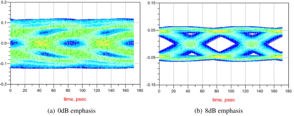
4.3 Transmitted waveforms for 0, 1, 2 to 6dB of de-emphasis . . . 43
4.4 Eye diagrams at the RX PHY using reference channel 1 . . . 43
4.5 Eye diagrams at the RX PHY using reference channel 2 . . . 44
4.6 CTLE settings . . . 45
4.7 Insertion loss of channel plus CTLE . . . 46
4.8 Reference Channel 1 CTLE equalization . . . 47
4.9 Reference Channel 2 CTLE equalization . . . 47
4.10 Insertion loss of 2 Channels in a series . . . 48
4.11 Eye diagram with 2 reference channel 2 in series emphasis of 8dB . . . 49
4.12 Verilog A CTLE Model . . . 50
4.13 Magnitude, phase and overall Deviation between Hspice and S parameter models 51 4.14 Verilog A CTLE Model . . . 52
4.15 Reference channel impulse responses . . . 52
4.16 Decision feedback equalization filter structure . . . 54
4.17 Eye diagram after the inclusion of a 1 tap DFE with optimized tap value(c1=-0.025,and 1dB of boost from the CTLE) . . . 56
4.18 Decision feedback equalization simulation . . . 58
4.19 Decision feedback equalization simulation . . . 58
5.1 Voltage histogram algorithm . . . 63
5.2 Voltage histograms after the CTLE when applied the 16 boost settings . . . 64
5.3 Sensitivity of the histogram algorithm to the number of histogram bins . . . 65
5.4 Voltage histogram algorithm sensitivity to the number of sample phases . . . 65
5.5 Histogram algorithm sensitivity to the number of total samples . . . 66
5.6 Voltage distribution of transmitted data . . . 67
5.7 Relation between eye opening and peak to peak Jitter . . . 69
5.8 Edge histogram calculation . . . 69
5.9 Edge histogram results for the adaptation of the CTLE . . . 70
5.10 Eye diagram for a 1 tap DFE:No tap vs optimum tap value . . . 71
5.11 Eye diagram for 1 tap DFE with negative tap values . . . 71
5.12 Received voltage histogram . . . 72
5.13 Edge histogram results . . . 73
5.14 Modes of operation for the DFE . . . 74
5.15 Error calculation with sign and traditional LMS in DFE . . . 75
5.16 Adaptive DFE simulation setup . . . 76
5.17 Reference channel 1 and 2 impulse response . . . 77
5.18 LMS algorithm applied to a 3 tap DFE . . . 78
5.19 Tap evolution with (from top to bottom) CJTPAT, CRJPAT,PRBS9 . . . 79
5.20 Taps evolution for training and decision direct for reference channel 1 and 2 . . . 80
5.21 Taps evolution using traditional LMS and sign(e) LMS . . . 81
5.22 Tap evolution with µ = 0.0025, 0.005, 0.0075, 0.01, 0.0125 . . . 82
3.1 High speed bit Rates . . . 30
3.2 Results for the Eye diagram simulation channel 1 . . . 37
3.3 Results for the Eye diagram simulation channel 1 . . . 38
4.1 Eye diagram measurements at the Rx-PHY while using reference channel 1 . . . 44
4.2 Eye diagram measurements at the Rx-PHY while using reference channel 2 . . . 44
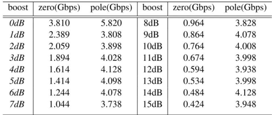
4.3 Location of the 1st pole and zero for different CTLE boosts . . . 46
4.4 Results for CTLE eye opening channel 1:no CTLE vs Optimum setting . . . 47
4.5 Results for CTLE eye opening channel 2:no CTLE vs Optimum setting . . . 48
4.6 Eye diagram after CTLE compensation with 2 channels in series -De-emphasis 8dB 49 4.7 ISI variation for different CTLE settings for reference channel 1 . . . 53
4.8 ISI variation for different CTLE settings for reference channel 2 . . . 53
4.9 Channel 1 Eye diagram stats for the inclusion of the DFE . . . 55
4.10 Channel 2 Eye diagram stats for the inclusion of the DFE . . . 55
4.11 Channel 1 Eye diagram stats for the inclusion of the DFE . . . 56
5.1 Eye diagram statistics . . . 63
5.2 mismatches between 0’s and 1’s in function of the CTLE boost and sampling phase 68 5.3 Eye diagram statistics for the inclusion of 1 tap DFE . . . 72
5.4 Mismatches between 0’s and 1’s in function of the DFE tap value and sampling phase . . . 73
5.5 Impulse response statistics for DFE adaptation . . . 77
ADS Advanced Design System CDR Clock and data Recovery CJTPAT Compliance Jitter Test Pattern CRPAT Compliance Random Pattern CTLE Continuous Time Linear Equalizer DFE Decision Feedback Equalizer FIR Finite Impulse Response Gbs Gigabit per Second IIR Infinite Impulse Response IP Intellectual property ISI Inter Symbol Interference LMS Least Mean Squares
MLS Maximum Length Sequence
MLSE Maximum length Sequence Estimation PHY Physical layer in the OSI model PRBS Pseudo Random Binary Sequence RF Radio Frequency
RX Receiver chip TX Transmitter chip UI Unit Interval
ZF Zero forcing algorithm
Introduction
The area of equalization has become a major area of research in the last couple of years due to the increase in the bit Rates used in serial communication interfaces. This increase led to the neces-sity to every communication interface to have some sort of equalizing circuit to compensate the distortion caused by the channel.
Many studies and articles have focused in the implementation of equalizer circuits, [3] discusses about the advantages of using a CTLE to perform cable equalization at 10Gbs. Article [4] ad-dresses a equalizing system with a CTLE and a DFE but both filters are static and the system does not include an adaptive algorithm. In [5] the adaptation of a DFE and CTLE for the PCIe inter-face at 8Gbs using algorithms like the Zero forcing and performing adaptation using an on chip eye monitor is discussed, however adaptation using these algorithms is usually very slow and the target bit Rate is inferior to the one used in the studied interface.
Another interesting fact is the possibility to implement a blind adaptation algorithm for the adap-tation of the DFE. In these kind of algorithms the receiver has no previous knowledge of the transmitted sequence and thus has a more difficult task to estimate the amount of channel induced ISI that needs to be compensated.
Article [6], talks about the use of the constant modulus algorithm in the DFE. However the article is only focused on the mathematical implementation of the algorithm and does not give an actual example of a real implementation.
This dissertation is focused on implementing an equalization architecture combining a CTLE and a DFE to perform channel equalization at 12Gbs and provide algorithms to adapt both filters to the transmission environment.
The tested algorithms should be as simple as possible to not disturb the interface specifications and should not require the insertion of many additional circuits to the interface.
1.1
Motivation
With the increase in communication speed for the serial interfaces the channel limitations become even more severe and the need of equalization becomes imperative.
One of main techniques of performing equalization in interfaces consists in placing a continuous time Linear Filter capable of compensating the high frequency losses of the channel.
The Decision feedback equalizer is also one of the equalizers that present better results in the elimination of inter symbol interference.
Although the theme of equalization of communication interfaces is a highly studied subject, the choice of the equalization architecture and adaptive algorithm are still very dependent on the in-terface and the channel to be compensated,with several known solutions.
Moreover, interfaces have specifications that need to be complied in order to be sold in the IC market and some equalization strategies comprise timing and power constraints that may not be compatible with the protocol specification.
So, the objective of this dissertation is to assess adaptive algorithms for the equalization filters present in the interface, these algorithms need to comply with the protocol specifications and must take advantages of specificities of the interface.
One of the main challenges of this work is the implementation of an algorithm that is capable of optimally adjust a CTLE and a DFE in the most simple fashion and with the minimum overhead possible.
1.2
Objectives
The work is focused on the study of both analogue and digital equalizers designed for the compen-sation of communication channels used in inter chip communications. The study will approach the following topics:
• Continuous Time Linear Equalization: Design of the filter and implementation of an adap-tive algorithm
• Equalization through digital filter:study of both transversal and decision feedback equaliz-ers.
• Study of the impact of each equalizer in the compensation of the communication channel. • Study of algorithms and implementations for automatic equalizer adaptation. Comparison
regarding performance and implementation cost. • Requirements for training sequences
1.3
Structure of the document
This document is structured in the following way :
Chapter 2 Gives a theoretical approach to the problems encountered when performing transmission at high speeds. This chapter explains in detail the problem of Inter-Symbol Interference and the use of equalization for the correction of channel induced distortion.
The chapter discusses equalization with a continuous time linear equalizer and with a deci-sion feedback equalizer explaining their working principle and their capabilities in correct-ing the channel Induced ISI.
The chapter also discusses techniques for the adaptation of these filters to the transmission environment.
Chapter 3 Describes the target interface that is proposed to host adaptive equalization. In this chapter are characterized the reference channels used to model the real transmission environment. Also in this chapter it is justified the need for equalization when performing transmission at 12Gbs and an architecture to compensate the reference channels
Chapter 4 Studies the impact of the equalization blocks in the eye diagram opening .
In this chapter a CTLE with 16 settings of boost using a two pole one zero transfer function is developed.
Chapter 5 Presents the use of different algorithms to perform adaptation of the equalization blocks, focusing in the adaptation of the CTLE and the DFE to the transmission environment de-scribed in chapter 3.Each algorithm is compared in terms of complexity, performance and time needed to perform adaptation.
Digital communication systems
Modern communication systems are based on digital transmission. The primary advantage over analogue systems is that digital signals are easier to regenerate and are more insensitive to noisy communication channels. In this chapter we will study factors that restrict the speed and reduce link quality in serial communication channels, the effects of band-limited problems are described using the Nyquist Criterium. Studying the methods that degrade the bit error ratio in a channel we can understand ways to improve or mitigate the influence of such factors, as for example using equalization.
Equalization can be accomplished using discrete or analogue filtering combined with methods to adapt these filters to the channel.It is necessary to compare these solutions in terms of complexity and efficiency.
Some approaches already implemented are given as an example to help the reader to further com-prehend ways to implement equalization filters in high speed links. Emphasis is given to imple-mentation and adaptation of both continuous time equalizers and decision feedback equalizers.
2.1
Inter-Symbol Interference
Several aspects degrade the probability of error in a communication channel, the channel itself has associated with it a frequency response usually similar to a low pass filter. The cut-off frequency associated to the channel is a function of the channel length, temperature among other variables. The maximum throughput that can be achieve in a communication is given by the Shannon-Hartley theorem, which states that the channel capacity C in bit/s is a function of the channel bandwidth in Hz and the signal to noise ratio:
C= B log2(1 +S N)
From the previous equation we can see that we want to make the channel bandwidth as high as possible so we can achieve the maximum throughput possible.
The channel transfer function is usually obtained by means of the Fourier transform, in the next figure we can view the usual low pass characteristic of a communication channel.
|Hc(w)|
w wc
Figure 2.1: Channel Low pass Transfer Function
The channel can both introduce Amplitude and Phase distortion altering the transmitted bits. For no amplitude distortion the channel transfer function Hc( jω) must be flat for the entire signal
spectrum.
| Hc( jω) |= K
For no phase distortion the channel group delay must be constant: −∂ Hc( jω)
∂ ω = K
As the channel introduces distortion the transmitted waveforms become attenuated, and dispersion causes the duration of the bit to be extended beyond T seconds. Dispersion of the signal can be caused by the distortion or by Multipath inside the channel.
t
T
T
tFigure 2.2: Bit distortion
When a sequence is transmitted through a channel that introduces dispersion inter symbol occurs.
Inter symbol interference results from the distortion of the waveform of the transmitted bits. Because bits interfere with the amplitude of neighboring bits in the sampling instant. ISI can cause the decision element to make incorrect decisions on the detection of a symbol.
2.1.1 Nyquist condition
Lets us consider that the channel is linear and time invariant, so it can be represented by its impulse response: Hc(n) = +L
∑
i=0 hkδ (n − k)δ (n) represents the Dirac pulse. The sequence observed after the channel results from the linear convolution of the input sequence and the channel impulse response:
y(n) = x(n) ∗ hc(n) y(n) = +∞
∑
k=−∞ x(n)hc(n − k)For no ISI one must satisfy the Nyquist criteria:
y(nT ) = (
c if n = 0 0 if n 6= 0
Nyquist criterium states that for no ISI the bit waveform can only be different from zero at is own sample time, this presents the Time domain Nyquist Criteria.
Considering that the received waveform y(t) equals:
yδ (t) =
+∞
∑
n=−∞y(nT )δ (t − nT )
yδ (t) represents the sampled received signal. Taking the Fourier transform we get:
Y δ ( f ) = 1 T +∞
∑
n=−∞ Y( f −n T) Because Y δ (t) = δ (t) −→ Y δ ( f ) = 1 +∞∑
n=−∞ Y( f −n T) = TThis equation represents the Frequency domain Nyquist Condition and it states that for no ISI the folded spectrum of the received signal must be constant.
Assuming a channel with bandwidth W , the Nyquist condition has the following implications: • Suppose that the symbol rate is so high that 1/T > 2W : no matter how the received spectrum
• If the data rate is slower then 1/T < 2W the copies of X(f) will overlap and there is many options for X(f) that make the folded spectrum ∑+∞n=−∞Y( f −Tn) flat.
Figure 2.3: Overlapping spectrum in the case of 1/T < 2W
• If 1/T = 2W Then the spectral copies of the bit waveform just touch and in order for not to exist ISI the spectrum Y ( f ) must be rectangular. A rectangular spectrum can only be achieve by shaping the bits as sync pulses. The rate 1/T = 2W is know as the Nyquist Rate and imposes the maximum theoretical bit rate that can be transmitted in a channel with bandwidth W.
2.1.2 Jitter
A finite bandwidth of the communication channels causing distortion is not the only factor that degrades the quality of a binary communication. In fact even if a channel satisfies the Nyquist condition the jitter alone can be a major limiting factor to the amount of BER.
By definition Jitter is the disturbance of the periodicity of the timing signals along the transmission path. Such disturbance can make the communication nonviable as the received waveform must satisfy both voltage and timing constraints.
For example in the extreme event of the peak to peak jitter reaching 0.5U I, meaning that each edge of a bit can drift at most 0.5UI, if the channel is ideal and does not introduce distortion the jitter alone will cause the receiver to make incorrect decisions as the sample time will drift to the adjacent bits.
Jitter can be divided into the following categories as stated in [7]
• Random jitter(RJ): characterized by a normal distribution described by its mean, usually zero, and by its RMS value
• Deterministic jitter(DJ): not described by a statistic distribution being characterized by its peak to peak value, it comprehending the following types :
– Data Dependent Jitter(DDJ):caused by the transmitted data patterns or due to cross talk
∗ Duty Cycle distortion(DCD): the timing of each bit changes along transmission ∗ Intersymbol Interference Jitter (ISIJ): the band limited channels cause that some
edge are faster or appear later than they should • Unbounded uncorrelated Jitter(UUJ): caused by cross-talk.
Jitter is a very complex phenomenon and can have many sources, and because of that its classification is many times done in a statistical way. Usually jitter is an intrinsic characteristic of every communication system and is a factor that should be expected and considered in the design of communication channels.In spite of this some jitter components can be minimized; for example ISI jitter can be reduced with TX and RX equalization
2.1.3 Scattering Parameters
Scattering parameters are used in radio-frequency engineering to describe the behavior of linear electrical networks operating at very high frequencies. The difference between S-parameters and other forms of representation like Y or Z parameters is that they do not represent the network in terms of currents or voltages, but in terms of behavior of power waves that pass through the network, another simplification introduced is that it considers that all the ports are properly termi-nated with a matched load (usually 50Ω). This comes from the fact that many times it is not easy to characterize a network in terms of current and voltages used in Y or Z parameters because there are not easy ways to produce an ideal short or open circuit in radio frequencies.So the S-parameter matrix describes a network expressing the behavior of a power waves that enter a port and exit a port.By convention the waves that enter a port are considered positive and the ones coming out are negative.Consider the following 4 port network:
[S]
a1 b11
2
3
4
a3 b3 b2 a2 b4 a4Figure 2.4: 4 port Network
The S matrix expresses the relation between the waves coming out and into a port:
b= Sa with S = S11 S12 S13 S14 S21 S22 S23 S24 S31 S32 S33 S34 S41 S42 S43 S44
We can define interesting quantities derived from the S parameter Matrix.
• Voltage Reflection coefficient as Sii
• Complex linear Gain e.g S13 Represents the complex gain between port 1 and 3 • Insertion loss is defined as e.g 20 log 10|S21|
• cross talk e.g S12 between port 1 and 2
In this section we presented a little review on S-parameters since often channels characteristics are represented in the form of an S- matrix.
2.1.4 Eye Diagram
The best way to measure the quality in communications links is the bit error ratio, but unfortunately such a measure cannot be easily measured, Specially during normal link operation.Eye diagrams present an easy and intuitive way to evaluate communication quality as they in a visual way lets us know how the distortion and jitter affect the signal waveform, following this approach eye opening is a good way to assure a low bit error ratio as a wider eye relaxes the receivers detector operating conditions for correct operation. An eye diagram is created by overlaying sweeps of different segments of a long data stream driven by a master clock, the next figure show us an example of an eye diagram. width height jitterPP rise time fall time SNR
Figure 2.5: Eye Diagram example
In the figure the parameter width represents the minimum time between two successive passes through the threshold voltage;
Heightgives us a measure of the difference between the peaks of a 0 level and a 1 level
Riseand fall time gives an average of the rising and fall time when the line switches voltage state SNRis a measure of the deviation of the level 1 and 0 voltage it indicates the amount of signal to noise Ration and distortion in the signal.
JitterPPor jitter Peak to peak gives us the maximum time diference between transitions by the voltage threshold.
Usually in a serial communication protocol, some minimum values for some of the previ-ous parameters are established forming an eye mask that determines the minimum quality for the communication to be considered viable. As said earlier the most important quality factor in a communication system is the BER.So how can we derive an approximation of the BER by using an eye diagram?
2.1.4.1 The Q factor
The article [8] gives a metric for the evaluation of the quality of the transmitted waveform by eval-uating the properties of the eye diagram. Consider the probability density functions at mean level 1 and mean level 0 to be a Gaussian distributed with an average µ1and µ0and standard deviation
σ1and σ1, respectively.
Let p(t0) and P(t1) be the probability of the occurrence of a bit 0 or a bit 1, and P(r0) and
P(r1) the probability of the detection of a bit 0 and 1 considering sampling in the middle of the
eye opening. We can define the probability of error as:
P= p(r0/t1) ∗ p(t1) + p(r1/t0) ∗ p(t0)
Where p(ri/t j) represents the conditional probability of detecting a bit i while transmitting a bit j. So the bit error ratio (BER) is given by:
BER=12er f(√Q 2) and Q = µ1−µ0 σ0+σ1 with: er f (x, µ, σ ) = 1 σ √ 2π Rx0 −∞e −(x−µ) 2σ 2
2.2
Strategies to mitigate ISI
In this section we will talk about strategies to fight Inter-Symbol Interference and improve link quality.
2.2.1 Fight ISI with bit shaping
We can deduce from the frequency Nyquist condition that bit shaping can help fight the effects of ISI in communication systems. The more we compress the signalling spectrum the higher the data rate we can transmit through a channel, the spectrum compression achieved by applying a Nyquist filter to the transmitting waveform. A widely used ISI free pulse is the raised cosine:
X( f ) = T for 0 ≤| f |≤ 1−α2T = 0 T 2[1 + cos π T α (| f | − 1−α 2T )] for 1−α 2T ≤| f |≤ 1+α 2T 0 for | f |> 1+α2T
α is the roll-of factor which determines the excess bandwidth from the original rectangular pulse 1/2T. The corresponding function is:
x(t) = sin πt T πt T cosπ αt T 1 −4αT22t2
α = 0 the raised cosine pulse becomes the sync function, 2.6and 2.7present the pulse shape and signal spectra of a raised cosine pulse as function of α.
Figure 2.6: Raised cosine waveform Figure 2.7: Raised cosine spectrum Notice that in the multiples of the sample period the waveform passes through zero resulting in zero ISI. Nyquist filters are hard to realize in practice because of their infinity impulse response. The roll-of factor decreases the ondulation after the time bit, which can be harmful for ISI if the sample time suffers from jitter.
2.2.2 Maximum length Sequence Estimation
In the maximum likelihood receiver the samples are not modified or reshaped by the receiver, instead using MLSE the receiver adjusts itself to better deal with the distorted samples. The MLSE receiver uses an estimate of the channel modelled as a finite input response (FIR) filter to compute the most likely transmitted sequence.
Let us consider the following channel model:
h
X
Y
Z
W
Figure 2.8: Discrete channel model.
X represents the transmitted sequence w represents white Gaussian noiseN (0,δ2) added to the channel.
yrepresents the output of the channel with impulse response h of length L. So from the above figure we can write z = y + w and y = x ∗ h resulting in :
yi= h0yi+ L
∑
j=1(hjxi− j)
The summation represents the inter symbol interference. In the MLSE receiver we want to maxi-mize the following expression:
P(Z | U(m∗)) = maxP(Z | U(m))
Meaning we want determine received sequence z that maximizes the probability P(Z | U(m)) U(m) represents a possible transmitted sequence.In the case of binary transmission and in the case of a transmitted sequence of size M. We have 2Lpossible sequences so the computational complexity increases exponentially with the sequence length M, making it impossible to use in real applica-tions.
2.2.2.1 Viterbi’s Algorithm
Viterbi’s algorithm uses a simplification of the MLSE algorithm and it takes advantage of a special structure called Trellis. The advantage of a Viterbi’s decoder compared with the original MLSE is that the complexity of the algorithm is not a function of the sequences length. The algorithm involves calculating a measure of similarity or distance between the received signal Z(ti) and all the trellis paths entering each state at time ti, discarding those trellis paths that could not possibly
be candidates to the maximum likelihood sequence. When two paths enter the same state, the path with best metric is chosen, the method is repeated for all the received bits.
Figure 2.9: Graphical illustration of the Viterbi’s algorithm(reprinted from [1]
In the diagram the dotted arrows represent the reception of a bit 0 and the other the reception of a bit 1.
The problem of Viterbi’s algorithm is that it requires knowledge of the channel transfer func-tion for the calculafunc-tion of the weight of each path. The number of operafunc-tions in the method grows linearly with the size of the sequence l, but the problem is the computation required to store and compute all the paths for the received sequence as the number of states increases with the size of the channel impulse response.
2.2.3 Equalization with Filters
In filter equalization the main idea is to compensate the channel impulse response Hc( f ) by in-troducing a filter He( f ) whose impulse response is the inverse of the channel. In this method the equalizer compensates the distorted pulses by reducing the effects of Inter Symbol Interference. Equalization with filters can be made in continuous or in discrete time where the compensation is done using samples of the received waveform. Equalization with filters can also be divided by the nature of their operation equalizing filters can be pre-set or adaptive. Pre-set means that the setup of the filter coefficients is only made at the beginning of the operation, adaptive requires the filter coefficients to be updated as operation takes place.
2.2.3.1 TX FIR equalization
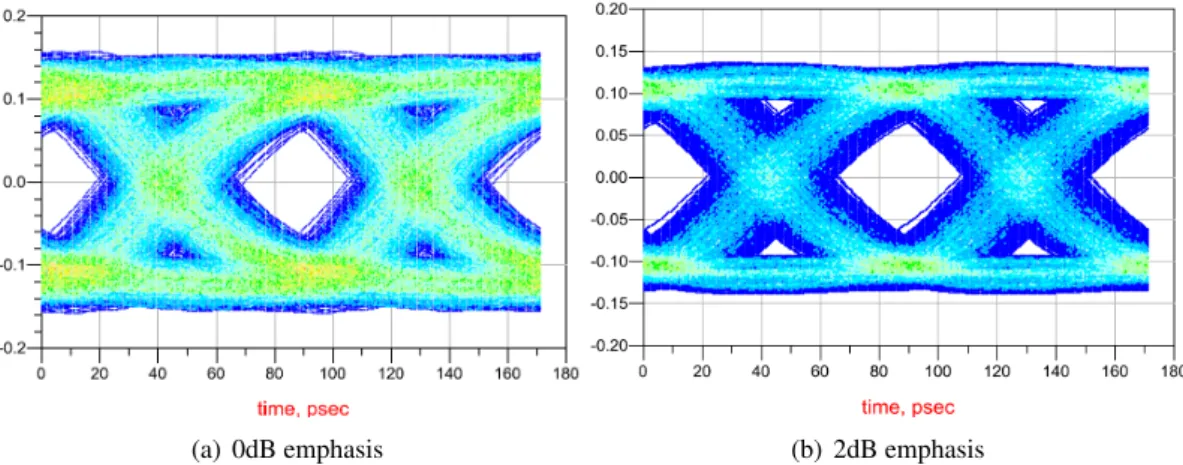
To perform pre equalization of the channel is usually place an FIR filter that pre-distorts the wave-form enhancing the high frequency content of the transmitting wavewave-form.This enhancement can be done using Pre-emphasis or De-emphasis. Using Pre-emphasis we increase the high frequency content of a signal relative to the low frequency content, de-emphasis decreases the low frequency content relative to the high frequency content. The amount of emphasis is usually specified in the value of the coefficients of the TX FIR filter. The following example shows the impact of the emphasis filter on the transmitted waveform.
The increase in voltage can be expressed as:
dbIncrease= 20 log(V2 V1)
The amount of voltage swings(difference between the voltages in the two differential lines) in the waveform is a function of the number of the taps of the equalizer
Number of voltages = 2number of FIR Taps−1
The number of taps in the Tx equalizer allows us to better compensate the overall frequency response,however the use of a big number of taps is not advised due to power restrictions in the equalizer.
Disadvantages of emphasis The emphasis process increase the signal edge rate which increases the cross-talk on the neighboring channels. Meanwhile, because pre-emphasis emphasizes the transition bits and de-emphasizes the remaining bits, if there is any discontinuity along the channel, the reflection at the discontinuity is more complicated to deal when using emphasis.
2.2.3.2 Continuous time linear Equalizers
In Continuous time linear equalizers (CTLE) equalizers the compensation is done by compensat-ing the channel attenuation at high frequency by introduccompensat-ing a high frequency boost, thus increas-ing the effective bandwidth of the channel.
H(j
w
)
w
Figure 2.11: Compensation Scheme
By increasing the effective bandwidth ISI becomes less significant and it reduces the probabil-ity of error. The increase of bandwidth is achieve with the introduction of a zero near the cut-off frequency of the channel :
He(s) = Ks+ ωz s+ ωp
Compensating with higher order systems with more than one zero can also be achieved but gener-ally with worse results, because phase linearity becomes an issue with higher order filters.
2.2.3.3 Circuit realization of CTLE
As we have seen earlier the desired response of the equalizer is a response with a zero and a pole.This is not possible due to the introduction of high frequency poles imposed by the electronic components. Equalizers are physically implement with a differential pair as seen in2.12:
Figure 2.12: Simple Equalizer schematic
Using simple circuit analysis we can observe that for low frequencies the circuit behaves as common source with source resistance, providing a DC gain equal to Rl/Rs. The high frequency
gain equals gmRl as the circuit behaves as common source amplifier. The position of the zero is
controlled by the capacity Cs and the value of the trans-conductance of the transistors of the differ-ential pair. The actual response does not stabilize at gmRl due to high frequency poles introduced by the parasitic capacitances of the transistors.
Other circuits derived from the previous are also used:
Figure 2.13: Equalizer Schematic reprinted from [9]
Figure 2.14: Equalizer Transfer Function reprinted from [9]
This circuit was presented for equalization at 3.5Gbits/s in [9] and the parameters of the equal-izer transfer function can be tuned by providing two control voltages, zctrl controls the frequency of the zero and Gctrl controls the initial Dc gain.
Figure 2.15: Equalizer schematic reprinted from [9]
This circuit, presents very low power consumption 2.46mW during normal function. The tuning of the equalizer is based in capacitive source degeneration and configures the CTLE gain with a variety of 8 different gain stages separated with a 1.5dBs increment.
The next circuit also allows the tuning of different high frequency boosts controlled with a control voltage V ctrl reprinted from [11]
2.2.4 Adaptation techniques for CTLE
In this section some adaptation techniques are studied for the tuning of the CTLE’s operation. As we discussed earlier the problem with CTLE’s is finding the equalizer transfer function that better compensates the high frequency loss presented in the channel so that:
Hc( jw)He( jw) = K, ∀ w(bit Rate/2)
So the adaptation algorithms must be able to tune the CTLE to better compensate the channel.
2.2.4.1 Asynchronous Under Sampling Histogram
Is based on the assumption that by under sampling the waveform after the CTLE and constructing a histogram based on the amplitude of the samples, we are able to evaluate the impact of the CTLE on the eye opening. The voltage histogram with lowest variance δ2 represents the better eye opening. Notice that the lower the variance the higher the peaking factor in the histogram.
Figure 2.17: Relation between eye opening and Under sampling Histogram (reprinted from [?] )
In a channel with no noise and no ISI the histogram would only present two peeks repre-senting the two voltages the "0" or the "1" bit. Adaptation following this method is theoretically simple, due to the existence of a small set of predefined coefficients for the equalizer. While in the adaptation period all the CTLE coefficients are tested and a histogram of the samples is made, the coefficients are selected so that the histogram with largest peak is selected. The problem with this approach is that the adaptation process usually takes some time, because we need to transmit a large sequence and analyze it to make the histogram a valid measure of the equalizer perfor-mance. In spite of this, this adaptation technique is one of the most widely spread for tuning CTLE coefficients due to its simplicity and low power circuit implementation.
2.2.4.2 Power Sensing
Adaptation through power sensing follows a different approach from the previous one. In this pro-cess the idea is to adjust the equalizer based on difference between the power of the high frequency and low frequency components of the received signal.
Figure 2.18: Adaptation using power sensing as described in [2]
In this scheme there are two different paths in the receiver the the unity gain path, and the high frequency boosting gain path, the boost gain control is controlled by the difference of powers between the received signal and the recovered signal after a regulating comparator. The power is detected with a filter followed by a rectifier and the difference of powers controls the position of the zero in the equalizer. Another more complete version of the adaptive CTLE is also presented in the same article.The new version also controls the gain at low frequencies 2.19.
2.2.5 Discrete Time Equalizers
In this section the compensation of ISI is accomplish using discrete filtering, we will discuss tech-niques of adaptation using training sequence and blind adaptation methods. In Discrete Time equalizer the compensation is based on the samples of the received sequence, as we seen earlier. If the impulse response of the channel is known the optimal receiver uses the MLSE method, but this method is not practical in very high speed communication due to the computation complexity of the algorithm.
Consider the following simplification of the discrete channel:
h
X
Y
Z
W
Figure 2.20: Discrete channel model
y(n) =
+∞
∑
k=−∞x(k)hc(n − k) and z = w + y
The idea is to introduce a filter in series with the channel so that: hc(n) ∗ he(n) = δ (n)
Taking the z transform results in:
He(z)Hc(z) = 1
Graphically the problem with discrete equalization can be resumed in figure 2.21:
Figure 2.21: Discrete equalization
2.2.5.1 Transversal equalizers
By the properties of the linear convolution we can see that for exact cancellation we need an IIR filter equalizer to make the perfect cancellation of ISI.
coefficients of a three tap equalizer that reduces the ISI.
By making the linear convolution, flipping and sliding the equalizer response over the channel response :
Figure 2.22: Convolution between equalizer and channel
We obtain the following equations for the overall response: he(0)hc(0) = 1 hc(1)he(0) + he(1)hc(0) = 0 he(2)hc(0) + he(1)hc(1) = 0 he(2)hc(1) 6= 0
If we consider he(0)=1 we get a value for the remaining ISI equal to hc(1)h(1)
2
h(0)2
For the case of a N tap equalizer and a two tap channel response we get the expression for the last tap of the overall response equal to:
ht(2 + N − 1) = he(1)he(1) he(0)
N−1
The transversal filter is one of the most popular form of an easy adjustable equalizing filter and the impulse response of the equalizer is the same as the filter coefficients
z(n) =
+N
∑
k=−NFigure 2.23presents the basic structure of a linear equalizer.
Figure 2.23: Linear equalizer
The transversal equalizer consists in a delay line with 2N T-second taps (T=symbol duration). The output of the equalizer is calculated through the weighted sum of the received samples by the filter coefficients, being the central the main contribution to the value of the output. The central tap corresponds to the current symbol to be calculated as other taps produce echoes to cancel the ISI in the current symbol.The basic limitation of the linear equalizer are that it performs poorly on channels having spectral nulls and the propagation of noise through the filter.
2.2.5.2 Zero Forcing equalizers
The Zero forcing equalizer makes the equalizer transfer function equal to the inverse of the channel transfer function in a limited number of points equal to the equalizer length:
He(z) = 1 Hc(z) In the zero forcing solution the coefficients are chosen so that:
z(k) = (
1 f or k = 0
0 f or k = ±1, ±2, ...., ±N
The number of taps of the equalizer equals 2N. In the zero tap equalizer one can only guarantee zero Inter Symbol Interference to the 2N adjacent bits of the sequence in relation to the current sampled bit.
Let us consider the following array definition: Z= z(−N) . . z(0) . . .z(N) C= c−N) . . c0 . . .cN X= x(0) x(−1) . . x(−N) x(1) x(0) . . .x(−N + 1) . . . . . x(N) x(N − 1) . . x(0)
Z represents a vector with the received samples to be presented to the element making the symbol decision.C is the array with the equalizer coefficients. X represents the samples present in the equalizer, X is a Toeplitz matrix. We can write the following equation:
Z= XC → C = X−1Z
By solving this equation we can make the ISI equal to zero in the 2N side lobes.
The length of the filter who performs zero forcing equalization is a function of the ISI introduced by the channel.
With a finite number of taps the ISI is minimized and the solution is optimal in terms of reduction of ISI at the sampling points. The ZF solution requires initial eye opening to perform equalization. The process uses a an estimate of the impulse response of the channel thus making it inappropriate for equalizing time variant channels.
2.2.5.3 Decision Feedback equalizers
One of main problem with the equalization using transversal filters was the impossibility of obtain-ing an IIR equalizer response, decision feedback equalizers can realize an IIR response because it uses both a forward and a feedback filtering paths. The idea behind the DFE is that if the values of the past decisions are known (decisions are assumed to be correct) then the ISI introduced by these symbols is subtracted to make the current decision. In the DFE the feedback filter uses previous quantized samples and because of this the output of the feedback filter is free of noise.
The sequence produced at the output of the channel equals: z(k) = y(k)hc0+
∑
j6=k
yjhck− j
The summation represents the ISI so the basic idea of the decision feedback equalizer is to simply subtract the ISI.
z(k) = y(k) −
∑
j6=k
yjhck− j
The transfer function of the DFE equals:
He(z) =
A(z) 1 + B(z)=
∑Mn=0anz−n
∑Nn=0bnz−n
Where bnand anrepresent the value of the coefficients of the feedback filter and transversal filter,
M and N is the size of the transversal and feedback filter.
Again the problem with equalization is to find the coefficients of both filter in order to achieve the best reduction of ISI fed into the decision device. Assuming that the output of the equalizer is given by: zk= 0
∑
j=−M yk− jhe, j+ N∑
j=1 zdk− jhe, jThe first summation gives the influence of the transversal filter on the symbol zk and the second the influence of the feedback filter on the output, note that the feedback filter uses already decided symbols zdk− jthus meaning that the feedback samples don’t have the influence of noise. Defining the following vectors:
IF =hzdk−1 zk−2d zdk+N−1 . . zdk−N iT IB=hyk−1 yk+N−1 yk+N−1 . . yk
iT hE, B =hhE,−M hE,−M+1 . . hE,0
iT hE, F =hhE,1 hE,2 . . hE,N
iT Where:
• IF represents the vector with the previous N decisions
• IB represents the vector with the M samples at the entrance of the equalizer • hE B represents the transversal filter coefficients
• hE F represents the Feedback filter coefficients
The filter coefficients are chosen to minimize the square error function E[Zk − X k]2. Resulting in the optimal filter coefficients:
hE, B = (E(IBIBT) − E[IBIFT]E[IFIBT])−1E(IFIK) hE, F = −E[IFIBT]hE, B
Where E denotes expectation. If we not know the value of the expectation values á priori we can estimate them using alternate process as we will see next.
2.2.5.4 Adaptation of discrete equalizers
As operation takes place the channel characteristics change. The optimum equalization parame-ters that were calculated at the beginning of the transmission might not be optimum later on. One solution would be to update the equalizer coefficients with periodically, but the majority of adap-tation algorithms needs the transmission of a training sequence that would consume much time that could be used transmitting necessary information.
The tap weights of the equalizer can be updated periodically or as operation takes place being referred as decision directed. Decision directed equalization tries to minimize the error between the output and input of the decision element to adjust the feedback filter coefficients. The decision direct technique can have problems with convergence if the eye at the input of the equalizer is initially closed. In this case, the equalizer taps need to be initialized using an alternate process . Let us consider the following structure of a system with adaptive equalization
Channel Adaptive Filter
Decision delay dn Xn Yn train Decision Direct en
Figure 2.24: Adaptive equalization structure
Figure 2.24 represents the usual adaptation process done in two stages, first calculate the initial coefficients of the equalizer with a training sequence and then switch to decision directed mode.
We see that the adaptive filter is updated using an estimate of the error signal [d(n) − y(n)]. The most common method for adaptive equalization is know as the Least Mean Squares Algorithm (LMS).The LMS algorithm consists on the minimization of the quadratic error between the desired response and the signal before the decision device. Let us consider the following model that uses the least mean squares algorithm to adapt a transversal filter to the channel:
hc(z) Channel A(z) Adaptive Filter dn Xn Yn en
Figure 2.25: Adaptive equalization scheme with transversal filter
ε = E[e2[n]] = E[(d[n] − y[n])2] By the properties of the expected value we get:
ε = E[d2[n]] + E[y2[n]] − 2E[y[n].d[n]]] In the case of no feedback structure the quadratic error becomes:
y(n) =
N
∑
j=0cjx(n − j) = cTx(n) −→ ε = E[d2[n]] − 2cTp+ cTRc
In this equation the quadratic error is a dependence on: • E[d2[n]]: variance of the desired response
• 2cTp: where p represents the cross correlation between the desired response and y(n)
• cTRc: where R represents the self correlation of y(n)
Notice that the expression makes perfect sense, as the quadratic error increases with the cross correlation between the desired response and the the output of the equalizer, meaning that the equalizer already reached a state where its transfer functions is the inverse of the channel. The expression encountered before defines the dependence of the quadratic error as function of the filter coefficients and its called performance surface.
The perfect equalizer is found when the quadratic error is minimum for that coefficients. So we define the gradient vector as:
∇(ε ) = ∂ E[e
2(n)]
∂ c = −2p + 2Rc The local minimum is found when ∇(ε) = 0
copt= R−1p; εmin= E[d2(n)] − pTcopt
Now considering that the coefficients are being updated in time we can define the update dynamics as function of the gradient of the quadratic error:
c(n+1)= c(n)− µ∂ E[e
2(n)]
∂ c
⇔ c(n+1)= c(n)− 2µE[e(n)x(n)]
This is know as the gradient algorithm, where µ represents the adaptation step. The problem with the gradient algorithm is the calculation of the estimate of E[e(n)x(n)] so the LMS algorithm uses a simplification that consists in replacing the average values of e(n) and x(n) by their instant values witch results in:
c[n+1]= c[n]− 2µe(n)x(n) , 0 < µ <
1 NE[x2(n)]
2.2.5.5 Adaptation of Decision Feedback Equalizers
The adaptation of the DFE can be made using the LMS algorithm seen earlier. The LMS algorithm tries to reduce the quadratic error between the desired response and the response at the entrance of the decision element. The DFE can work in one of two modes, training mode or decision direct mode. c1 c2 c3 z z-1 -1 -1 z xn yn yn-1 yn-2 yn-3 fs en delay train sequence
Figure 2.26: Training mode
c1 c2 c3 z z-1 -1 -1 z xn yn yn-1 yn-2 yn-3 fs en
Figure 2.27: Decision Direct mode The expression for the coefficient adaptation can be expressed as :
c(n+1)= c(n)− 2µe(n)y(n − 1)
Lets analyse this equation more carefully as it is the core of LMS adaptation.
If the error is calculated based on the receiver having a replica of the transmitted sequence and simply calculating the difference between the transmitted bit and the value that is at the entrance of the decision element, the equalizer knows the effects of the channel on the transmitted bit and can calculate the coefficient taps that best compensate distortion. If the equalizer on the other hand is working in decision direct, if the decision element makes the wrong decision, the equalizer will be working on the assumption that the distortion suffered by the bit is different from the reality, this will cause the equalizer to converge to an improper value. On the other hand the information that is sent is also an important factor, as the equalizer taps will converge to the value that best compensates the distortion caused by the channel in that particular sequence used in the training. So in order to better train the equalizer the training sequence must be as random as possible to better adapt the equalizer to the channel and not to that particular sequence. The simplification used in LMS for the value of the gradient makes that the coefficients do not converge to the optimal solution instead it oscillates around it. This oscillation is called Gradient noise. Other algorithms use different approaches for the calculation of the gradient and can make the adaptation step variable, despite all, the LMS is the most used due to its simplicity and easy implementation. To decrease the computation to implement the LMS some simplifications can be made in the original expression for the error calculation, in the next example is shown the coefficient update equation for the sign LMS:
c(n+1)= c[n]− 2µe(n)y(n − 1) c(n+1)= c[n]− 2µsign(e(n))y(n − 1) sign(x) =
(
1 f or x > 0 −1 f or x < 0
This simplification implies that the taps of the equalizer will converge always with fixed step µ and will only converge for the value of the post-cursor ISI, if the channel introduces decision errors. As the step size is fixed and the error is binary, the implementation becomes severely simplified at the cost of convergence speed and steady state error.
2.3
Final remarks
In this Chapter we reviewed some important topics about aspects that degrade communication quality in high speed serial interfaces and the need of equalization to reduce the effects of channel distortion and jitter in binary transmission
The focus of the study was on techniques to implement and adapt CTLE and a DFE to the trans-mitting environment.The method of asynchronous under-sample Histograms showed promising results in the adaptation of a zero pole and two pole linear equalizer.The LMS algorithm also proved to be a possible solution to the adaptation of a decision feedback equalizer. In the next chapters a study of the applicability of these techniques to the implementation of adaptive equal-ization in a high speed interface will be conducted.
System Specification
As mobile industry continues to increase, companies in order to succeed in such competitive mar-ket need to provide the customers products with the best technologies in the marmar-ket at the lowest costs possible. The increase in processor computation power brought the increase in complexity of mobile phones, that today offer functionality which are closer to a computer than to a simple phone. The increase in computation power was kept up with the evolution of peripheral such as cameras and displays. This led to the urge of the establishment of a protocol that could connect a high variety of peripherals with the processor in mobile devices. Such protocol would need to be flexible to be easily adapted to multiple interfaces, transmit at a high bit Rate to serve the high speed requirements of some applications and yet maintain a low power consumption required by the mobile industry. This protocol became a standard in mobile devices for the communication in system–on-chips ranging from smartphones, tablets and notebooks, the protocol established standards both in hardware and in software allowing the creation of hardware products that work seamlessly with numerous processors and components from multiple vendors.
Synopsys is one of the major contributors to the diffusion of this protocol in mobile industry, pro-viding IP (controller + physical layer) solutions to its clients. This IP will serve as the basis for the establishment of more complex protocols that benefit from the abstraction provided.
This work is focused on the study and implementation of a architecture of adaptive equalization for the physical layer associated with the referred protocol. The rest of this chapter will provide an additional insight on the physical layer studied denominated from now on as PHY.
3.1
The PHY
As said earlier Synopsys offers solutions as a combination of a physical layer denominated as the PHYand a controller that interacts directly with the PHY. The PHY is a physical layer optimized for high speed and low power operation. The flexibility of being used in multiple applications is introduced by the ability of the PHY to switch between high speed mode and low power mode in only a few micro seconds.
3.1.1 Architecture of the PHY
The PHY can work both in Mesochronous and Plesiochronous clock mode because of the capabil-ity of performing both phase and frequency recovery. The PHY clocking flexibilcapabil-ity makes it even more suitable for a larger number of operations, as the receiver and the transmitter do not need to share the same reference clock.
The PHY can have multiple data Links and each link has a TX and a RX which is fixed (one must define the direction data flow).Each link has its own configuration settings. By configuring how many links are transmitting and at what bit Rate, the PHY can be a very physical layers as one can further trade-of easily between link bandwidth and power consumption. The following picture demonstrates a typical mode of operation between two PHY’s.
RX-phy
TX-phy
Chip_A
Chip_B
link 1 link 2 link nFigure 3.1: Typical PHY mode of operation
The PHY supports two main transmission modes: Low speed mode supporting bit Rates from 3Mbps to 0.5Gbps and High Speed mode with bit Rates that are expected to reach the 12Gbps.
The following table shows the bit Rates used in high speed(HS) mode. Table 3.1: High speed bit Rates
Type A(Gbps) Type B(Gbps)
HS Bit Rate 1 1 1.5
HS Bit Rate 2 2.5 3
HS Bit Rate 3 5 6
HS Bit Rate 4 10 12
The transmitted waveform consist in a differential signal with configurable differential volt-ages, common mode voltage and configurable bit Period. These settings are chosen accordingly to the current mode of operation and physical characteristics of the channel.
3.1.2 Characterization of the PHY
In this section we will study the characteristics of some blocks present in the PHY, both in the TX and in the RX, the study will obviously be focused in blocks that are relevant for the theme of the work. This information is necessary because it is important to know the environment in witch the adaptive equalization will be implemented.
3.1.2.1 Characterization of the TX-phy
In the following image is a highly simplified version of a block diagram of a TX block of the PHY.
Serializer Emphasis Filter clk Driver Term data<x:0> 8b10b
TX
Figure 3.2: Block diagram of the TX PHY
The transmission block consists of:
• Term: line termination, adapted to the channel to avoid reflections. • Serializer: To performs parallel to series conversion.
• PLL: To Generates the reference clock for transmission. • Emphasis Filter: Performs Tx equalization
• Driver: Outputs the sequence for transmission. • 8b10b: Performs 8b10b conversion in the bit stream.
The termination of the line is configurable by the PHY. The value of the termination influences the differential voltage of the transmitted signal,a non terminated line requires a higher differential and common mode voltage. The emphasis filter consists in a 3 tap FIR filter designed to pre-distort the bit stream emphasizing the high frequency components of the transmitted sequence.
The 8b10b block performs line coding conversion to achieve DC balance of the transmitted wave-form and to provide the receiver with more edges to improve clock and data rate recovery (CDR).
3.1.2.2 Characterization of the RX-PHY
In the following image is a highly simplified version of a block diagram of a RX block of the PHY.
GainX&XCTLE DataXSlicers DFE DeXSerializer
10b8b
CDR PLL
data<x:0>
RX
Figure 3.3: Block diagram of the RX PHY
The RX block consists of:
• Term: line termination, adapted to the channel to avoid wave reflections.
• Gain & CTLE:The CTLE performs analogue RX equalization increasing the high frequency components of the received signal. The Gain increases the signal power for proper detection. • Data Slicer: Sample the Input Waveform at a rate given by the local reference clock. • DFE: Performs RX Digital Equalization of the sampled waveform.
• CDR: Performs clock and data recovery based on received waveform.
• PLL: Generates a reference clock based on the clock estimation given by the CDR block for sampling the input data.
• De-Serializer: performs series-parallel conversion.
The RX CDR performs clock and data recovery block has a circuit capable of generating several clock phases used to perform CDR. The presence of this clock references will help in the task of adapting the CTLE as we will see later on.
3.2
The transmission environment
3.2.1 Transmission environment S-Parameters Simulation
The usual application of the protocol in question is in the transmission between two integrated circuits inside a PCB board.
The losses and distortion that the signal suffer are mainly attributed to the losses in the PCB trace that connects the two chips and their packages.
phy
IP phyIP
chip B
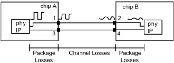
Channel Losses Package Losses Package Losses 1 2 3 4 chip A
Figure 3.4: Schematic representing the connection between two chips with port identification.
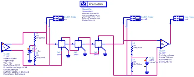
Both the channel and packages responses were described with S-parameters. For the package and channels the models were constructed by inspection in the laboratory using a Vector Network Analyser(VNA)during the interface testing. The network analyser works by applying a series of sinusoidal stimuli at each port and measuring the magnitude and phase response at every other port of the network under study.By sweeping the frequencies of the stimula the device can build a sampled description of the network with S-parameters. The process produces a .snp file, giving for each point of frequency the magnitude and phase of every element of the S matrix for a n port network. By analysing the content of the .s4p file in ADS, it was observed an expected symmetry in terms of the S matrix, as a result of the intrinsic symmetry of the electrical circuit being anal-ysed. For example the transmission coefficients S12and S34and similarly the reflection parameters
show approximately the same frequency behaviour for both input ports. Having this in mind from now we will only analyse the S-parameters for one input Port.
The following figures were obtained in ADS by performing S parameter simulation for the refer-ence package used by the Interface.
(a) Insertion Loss S12 (b) S11S13S14
The frequency behaviour of the package insertion loss is quite good presenting a loss of less than 0.5 dB at 10 GHz. The reflection and the effects of cross talk increase with frequency. In fact the reflection coefficient reaches the −10 db at about 12 GHz. This aspect does not seems critical since at the Nyquist frequency of the highest bit rate (6 GHz) the packages does not introduce a large amplitude distortion.
Next we will analyse the response for both reference channels following the same methodology. Reference channel models are used to characterize the medium used to connect two chips using the PHY physical layer. Reference channel 1 and 2 set both of the extreme conditions for attenuation and phase response we need to consider for the characterization of the transmission environment. Figure 3.6 3.7present the results for the S parameter simulation of both reference channels. First we analyse the insertion loss and then we analyse the reflection coefficient and the effects of the cross talk separately.
(a) Insertion Loss S12 (b) S11S13S14
Figure 3.6: Reference channel 1 S-parameter simulation results
(a) Insertion Loss S12 (b) S11S13S14
If we focus our attention on the insertion loss of both channels we can see that reference channel 1 presents a notch at the frequency of 4.450 GHz where the insertion loss reaches the −41.449 dB. Reference channel 2 also presents a notch but at an earlier frequency of about 1.950 Ghz with the insertion loss reaching −38 dB.
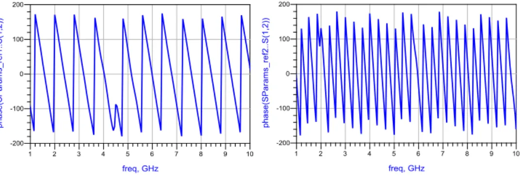
The worst behaviour observed in reference channel 2 corresponds to a PCB trace of longer dimen-sions than the one of the model of channel 1. Now we will take a closer look at what happens in terms of phase of the Insertion Loss for both channels.
(a) Reference channel 1 S12 (b) Reference channel 2 S12
Figure 3.8: Phase of the insertion loss for reference channel 1 and 2
Observing figure 3.8, we notice the effects of the notches of both channels cause an inversion of the phase behaviour,introducing phase distortion. The behaviour near the notch, both channels is almost of linear phase. It is not expected that phase distortion to be a major issue while trying to perform equalization. From the phase of the insertion loss we can estimate the delay caused by each channel to be: ∂ −6∂ f(S12)
![Figure 2.18: Adaptation using power sensing as described in [2]](https://thumb-eu.123doks.com/thumbv2/123dok_br/18894922.934469/39.892.221.682.326.563/figure-adaptation-using-power-sensing-described.webp)