Design of DC-3.4GHz Ultra-Wideband Low Noise Amplifier with
Parasitic Parameters of FET
Yinhua Yao*, Tongxiu Fan**
*(No.36 Research Institute of CETC, Jiaxing Zhejiang 314033, China) ** (No.36 Research Institute of CETC, Jiaxing Zhejiang 314033, China)
ABSTRACT
This paper presents two low noise amplifier (LNA) circuit topologies for ultra-wideband wireless
communications in 0.13μm PHEMT GaAs technology. They are with source inductive degeneration and source
grounded, respectively. The simulation results show that the LNA involving source inductor possesses good
performances at 120MHz-3GHz. Its noise figure(NF) and voltage standing wave ratios(VSWRs) are less than
1.173dB and 2, respectively, while the maximum gain of 12.75dB is achieved with 0.63dB flatness. In contrast, the other LNA provides a decreasing gain varying between 10.992dB and 11.964B in a wider frequency range
of DC-3.4GHz. NF and VSWRs are better than 1.287dB and 2, respectively.
Keywords
-
Low Noise Amplifier, Resistive Feedback, Source Inductive DegenerationI.
INTRODUCTION
Low noise amplifier (LNA), one of the most important analogy blocks in wireless communication
systems, must be broadband matched to a 50Ω
antenna. In addition, it must provide a high voltage gain on a high impedance value capacitive output load, while adding as little noise as possible [1]. Moreover, it should be linear enough to handle strong
interferers without introducing intermodulation
distortion [2].
As operating frequency increases, the effects of FET parasitic parameters, especially source parasitic inductor Ls, on performance can no longer
be neglected. As well known to us, an additional source inductor enhances stability and achieves noise matching and good linearity. Yet, its small inductance can not be controlled easily in practice. Also, a small change in the inductance has a significant impact on gain, stability, and noise figure
(NF) of LNA [3, 4]. Excessive source inductance can
lead to LNA oscillations because of gain peaks at higher frequencies [5]. Therefore, if the potential source inductor Ls are not taken into consideration
during simulation, it will influence the practical performances significantly. However, there are few papers concentrating on this issue.
Broadband LNA is a challenging in software defined radio (SDR)[6], and the main challenge in design such wideband LNA is to make it able to work from hundreds MHz to several GHz. In this paper, two ultra-wideband LNAs operating at 120MHz-3GHz and DC-3.4GHz respectively are presented for wireless communication systems. For better designing LNA, the parasitic parameters of FET, such as gate parasitic inductor, gate-to-source
capacitor, and source parasitic inductor, are taken into consideration. At the same time, the effect of additional source inductor on the performance of LNA is investigated. In order to implement subsequent layout, the transmission lines between two elements are also considerad using microstrip
lines with 50Ω characteristic impedance during
simulation, but they will not be discussed below.
II.
C
IRCUITD
ESIGNAn extrinsic GaAs FET high-frequency model which includes parasitic elements is shown in Fig. 1.
Fig. 1 A microwave GaAs FET common-source model that includes parasitic elements [7]
The meaning of the parasitic elements Cds,
Cgs, Cgd, Rg, Rs, Rd, Lg, Ls, and Ld is self-explanatory.
For GaAs MESFET with 1μm gate length and 25μm
gate width, Cgs =0.3pF, Cgd =0.02pF, and Cds
=0.05pF. Generally, for a packaging FET, the typical values of parasitic inductor and resistor are 0.1-0.9nH
and 0.1-0.2Ω. In this paper, for simplicity, their
values are set as 0.1nH and 0.15Ω, respectively. ri
and rdsare the small gate-to-source channel resistance
and the big drain-to-source channel resistance, respectively, which can be neglected.
The LNA design is based on CGY2105XHV (OMMIC Co., Ltd.), which is an extremely low noise
figure amplifier with linearity suitable for
applications from 500MHz to 4000MHz. The MMIC is manufactured using OMMIC’s qualified 0.13μm PHEMT GaAs D01PH technology. The LNA is designed and simulated on Rogers 4003C dielectric substrate having a permittivity of 3.38, a thickness of 0.508 mm, and a loss of less than 0.0027.
2.1 LNA with source inductive degeneration
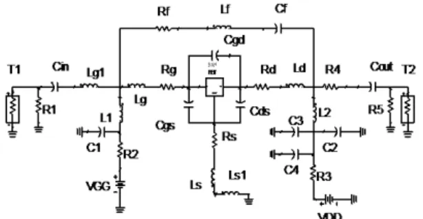
Fig. 2 shows the proposed common source LNA circuit topology with source degeneration inductor. The small inductor Ls1 with an inductance
of L nH, which can be replaced by a high impedance
microstrip line with a length of l mm according to the
following formula: r 0 81 . 11 Z L
l (1)
where Z0 is the characteristic impedance of the
microstrip line, and ris the relative permittivity of
the layout. The use of an inductive line with a high Z0
and short length achieves a good approximation of a lumped inductor [8].
Fig. 2 LNA with source degeneration inductor
Referring to the given circuit in manual, bias
circuit is designed. The LNA is biased at VDS=3V and
IDS=50mA with supply voltage VDD of +5V and VGG
of -0.58V. Shunt RC filter is introduced in the gate to improve the low-frequency stability of amplifier. In order to decrease its effect on NF, stable network should be connected to the drain of FET rather than to the gate [9]. The separation of RF signals from DC bias conditions is achieved through so-called radio frequency coils (RFCs).
For wideband LNA, input matching
topologies include resistive termination, common gate, and resistive shunt-feedback. Since the input of a CS MOS device is primarily capacitive, we can
terminate the input with a resistor R1. Although
greatly degrading the NF due to adding its own noise
and dropping the gain, resistive termination provides a good power matching [1]. Neutralization cancels
signal flowing through Cgd by adding a shunt
negative feedback path consisting of a resistor Rf, a
capacitor Cf, and an inductor Lf [10]. In addition,
good gain flatness can be achieved easily in a wide
bandwidth through introducing Rf in the feedback [7].
Furthermore, the feedback path also enhances the
stability of amplifier to some degree. Lf lessens
low-frequency gain, increases high-low-frequency gain, broadens waveband, and degrades the effect of transistor parameters on the amplifier [11].
When the GaAs FET is unconditionally stable in the frequency range of interest, the feedback capacitance Cgd is very small and can be neglected.
For simplicity, the effects of feedback path on the input and output impedances are ignored. And considering that inductors Lg1 and Ls1 are ideal, it is
easy to show the input impedance of the LNA given by [7]: gs s s m g s gs s m s s g g in C L L g R R C j R g L L L L j Z ) ( ) ( 1 1 1 (2)
The source impedance is expressed as:
in Source C j R R R Z 1 /
1 0 1
0
(3)
R0 is the signal source impedance, usually
50Ω. In order to realize input matching,
namely *
in
Source Z
Z , the values of Ls1, R1, Cin, and Lg1
are optimized and tuned. The output impedance of the LNA is:
5 4 1 || ] ) 1 1 ( [ R R R R C C L L L j Z d s ds out d s s out (4)
Due to Rs+Rd<<R4 and the dominant
) /(
1 Cout of terms in the parenthesis at DC-3.4GHz,
the output impedance can be simplified as:
)] ( ) ( 1 [ ) ( ) ( 1 5 4 2 4 2 5 2 5 4 2 5 R R R C R C j R R C R Z out out out out
(5)
When (Cout)2(R4R5)21 and
1 ) (
)
( 42 4 5
2 R R R
Cout
, which can be satisfied easily
by increasing the value of Cout, the output impedance
can be further simplified as:
5 4 5 4 2 5 4 2 5 )
( R R
R R R R C R j Z out
out
(6)
A good output matching and the maximum gain is achieved when R4R5/(R4+R5) approaches RL
(load impedance, usually 50Ω).
Noises from R4 and R5 are attenuated by the
LNA gain. Thus, the extrinsic noise sources are mainly associated with R1 and Rf, the increase in
which will enhance the NF. In addition, the
met, which ensure the unconditional stability of the LNA[11].
2.2 LNA with source grounded
The other LNA schematic with source grounded is shown in Fig. 3. Besides the same bias
circuit omitted here, this LNA has similar L-type
matching networks to the former one. What is the biggest difference between two LNA circuit topologies is the source grounded directly of this LNA, and Ls1 is replaced by L3. Similarly, the input
and output impedances of the LNA are written as:
gs s m g s gs
s m s g g in
C L g R R C j
R g L L L j
Z
( 1 ) (7)
5 4
3
|| ]
) 1 1 (
[
R R R R
C C L L L j Z
d s
ds out d
s out
(8)
Fig. 3 LNA with source grounded directly
The equation (6) still holds here when the hypotheses stated above are satisfied. The source impedance of this LNA can also be expressed by
equation (3). Comparing the formulae of Zin and
ZSource of two LNAs, it is noted that R1 in this LNA
should be larger to reach the input matching.
However, an increasing R1 brings about the negative
results as stated above. Seen from formulae (7) and (8), the input and output impedances are independent
each other, as a result of which, better VSWRs
representing impedance matchings can be obtained in this LNA. In the process of design, it is found that a small change in the values of parasitic parameters
except for Ls has ignorable effects on the
performances. This is in good agreement with the statement in Introduction Section, and it can be understood easily from equations (2) and (4) that Ls
affects both the input and output impedances. Besides, this LNA is also unconditionally stable due to Re(Zin+Zsource) and Re(Zout+ RL) above 0.
III.
S
IMULATIONR
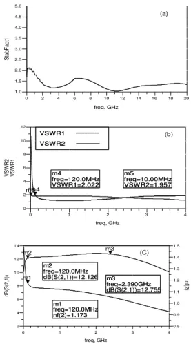
ESULTSFig. 4 illustrates the simulation results of LNA with source inductive degeneration. It can be seen from Fig. 4(a) that the LNA is unconditionally stable in full waveband (DC-20GHz), which is consistent with analysis before. Seen from Fig. 4(b),
output voltage standing wave ratio (VSWR2)is below
2 at the frequencies between 10MHz and 4GHz,
while input VSWR1 increases to 2.022 when the
frequency decreases to 120MHz from 4GHz. And the
good VSWR1 and VSWR2 are hardly obtained
simultaneously at frequencies lower than 120MHz. The reason is attributed to the effect of Ls1 and
inherent Ls. Based on the relationship between
VSWR1 and input reflection coefficient (S11), S11 is
below -9.4dB. Fig. 4(c) shows that the maximum
forward gain S21 is 12.755dB, and the minimum value
is 12.126dB over the frequency band of
30MHz-3GHz. NF less than 1.173dB also meets the specified
requirement across the desired frequency range.
(a)
2 4 6 8 10 12 14 16 18
0 20
1.5 2.0 2.5 3.0 3.5 4.0 4.5
1.0 5.0
freq, GHz
S
ta
bF
act
1
(b)
m4 freq= VSWR1=2.022120.0MHz
m5 freq= VSWR2=1.95710.00MHz VSWR1
VSWR2
1 2 3
0 4
2 4 6 8 10
0 12
freq, GHz
V
S
W
R
1
m4
V
S
W
R
2
m5 m4 freq= VSWR1=2.022120.0MHz
m5 freq= VSWR2=1.95710.00MHz VSWR1
VSWR2
(C)
m2 freq=
dB(S(2,1))=12.126120.0MHz m3 freq=
dB(S(2,1))=12.755 2.390GHz
m1 freq= nf(2)=1.173120.0MHz
1 2 3
0 4
4 6 8 10 12
2 14
0.9 1.0 1.1 1.2 1.3 1.4
0.8 1.5
freq, GHz
dB(S(2
,1
))
m2 m3
nf(2
)
m1 m2 freq=
dB(S(2,1))=12.126120.0MHz m3 freq=
dB(S(2,1))=12.755 2.390GHz
m1 freq= nf(2)=1.173120.0MHz
Fig. 4 Simulation results of LNA with source
inductive degeneration (a) stability factor(b) VSWRs
(c) S21 and NF
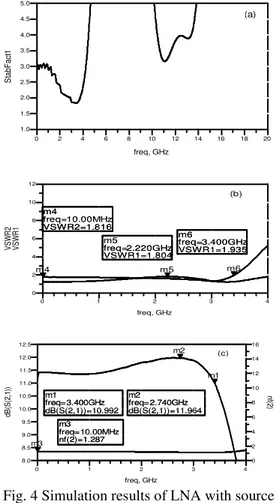
The simulation results of LNA with source grounded are depicted in Fig. 5. The LNA is also unconditionally stable, with a higher stability factor. In contrast, the LNA shows a little degraded but still satisfied performance even at the frequency lessening to 10MHz and climbing to 3.4GHz. The gain decreases by about 0.8dB, varying between 10.992dB
and 11.964dB. NF is below 1.287dB over the target
larger R1. Moreover, VSWRs are not more than 2 in
the frequency range of 10MHz-3.4GHz. According to the value of VSWR1, S11 is below -10dB. The curve
of VSWR2 is similar to the former one, which is
ascribed to the same approximated output impedance. Table.1 summarizes the performance of the LNA along with results from recently published papers.
(a)
2 4 6 8 10 12 14 16 18
0 20
1.5 2.0 2.5 3.0 3.5 4.0 4.5
1.0 5.0
freq, GHz
S
ta
b
F
a
ct
1
(b)
m5 freq= VSWR1=1.804
2.220GHz m6 freq= VSWR1=1.935
3.400GHz m4
freq= VSWR2=1.81610.00MHz
1 2 3
0 4
2 4 6 8 10
0 12
freq, GHz
V
S
W
R
1
m5 m6
V
S
W
R
2
m4
m5 freq= VSWR1=1.804
2.220GHz m6 freq= VSWR1=1.935
3.400GHz m4
freq= VSWR2=1.81610.00MHz
(c)
m1 freq=
dB(S(2,1))=10.992 3.400GHz
m2 freq=
dB(S(2,1))=11.964 2.740GHz
m3 freq= nf(2)=1.287
10.00MHz
1 2 3
0 4
8.5 9.0 9.5 10.0 10.5 11.0 11.5 12.0
8.0 12.5
2 4 6 8 10 12 14
0 16
freq, GHz
dB(S(2
,1
))
m1 m2
nf(2
)
m3 m1 freq=
dB(S(2,1))=10.992 3.400GHz
m2 freq=
dB(S(2,1))=11.964 2.740GHz
m3 freq= nf(2)=1.287
10.00MHz
Fig. 4 Simulation results of LNA with source
grounded directly (a) stability factor(b) VSWRs (c)
S21 and NF
Table 1 Performance summary of published CMOS LNAs
BW (GHz)
S21
(dB)
S11
(dB) NF (dB)
Topology
[6]
0.1-2.5
22
<-10
2-2.4 Feedback
[12] 0.5-7 22 <-9 2.3-2.9 Feedback
[13]
DC-11.5
13.2 <-8 5.6 Feedback
[14]
3.1-10.6
13.7-16.5
<-10
2.1-2.8 Feedback
[15] 0.6-6 17
<-10 2.3-2.96
noise-cancelling This
work
0.12-3 >12
<-9.4
<1.173 Feedback
This work
DC-3.4
>11 <-10.8
<1.287 Feedback
IV.
C
ONCLUSIONThis paper investigates the effects of source inductive degeneration on the performance of LNA, which involves parasitic parameters. The source parasitic inductor has a significant influence on the input and output impedances. In the 120MHz-3GHz band, the LNA with source inductor has a maximum gain of 12.755dB with a gain flatness of 0.63dB, a
noise figure less than 1.173dB, and VSWRs below 2.
In contrast, the other LNA with source grounded achieves reasonably acceptable performances in a wider frequency range of DC-3.4GHz. A decreasing gain of 11.964dB with a variation of 0.972dB is obtained, while the noise figure is no more than 1.287dB. Besides, the LNA accomplishes better input
and output matchings, and VSWRs are smaller than 2.
Compared with results published in previous studies, much lower noise figures are provided in this paper. Such LNAs can find wide application in software defined radio, receiver front-end, and other wireless communication systems.
R
EFERENCES[1] M. Battista, J. Gaubert, A. Fanei, Y.
Bachelet, M. Egels, P. Pannier, S. Bourdel, H. Barthélémy, and G. Bas, Design and implementation of ultra-wide-band CMOS LC filter LNA for carrier less
impulse radio receivers, Analog Integrated
Circuits and Signal Processing, 65(3),
379-388.
[2] S. Andersson, Multiband LNA Design and
RF-Sampling Front-Ends for Flexible
Wireless Receivers, master diss., Linköping
University, Sweden, 2006.
[3] B. M. Liu, C. H. Wang, M. L. Ma, and S. Q.
Guo, An voltage and
ultra-low-power 2.4GHz LNA design,
Radioengineering, 18(4), 2009, 527.
[4] R. C. Liu, C. R. Lee, H. Wang, and C. K.
Wang, A 5.8GHz two-stage high-linearity
low voltage low noise amplifier in a 0.35μm
CMOS Technology, Proc. IEEE Radio
Frequency Integrated Circuit Symposium,
Seattle, WA, USA, 2002, 221-224.
[5] A. P. Adsul and S. K. Bodhe, Performance
Evaluation of Different LNA’s having Noise
Cancellation and Phase Linearity
Characteristics for IR-UWB Systems,
International Journal of Engineering and
Technology, 3(6), 2011-2012, 419-428.
[6] M. Ingels, C. Soens, J. Craninckx, V.
Giannini, T.Kim, B. Debbaillie, M. Libois, M. Goffoul, and J. V. Driessche, A CMOS 100MHz to 6GHz software defined ratio analog front-end with integrated pre-power
Circuits Conference, Munich, 2007, 436-439.
[7] G. Gonzalez. Microware transistor
amplifiers analysis and design (Prentice
Hall/Pearson, 2003).
[8] J. S. Hong and M. J. Lancaster, Microstrip
filters for RF/microwave applications (New
York: John Wiley ﹠Sons, Inc, 2001).
[9] J. B. Xu, Research of Ka-band broadband
Monolithic Low Noise Amplifier, master
diss., Nanjing University of Science & Technology, Nanjing 2007.
[10] D. J. Cassan and J. R. Long, A 1-V
transformer-feedback low-noise amplifier
for 5-GHz wireless LAN in 0.18μm CMOS,
IEEE Journal of Solid-State Circuits, 38(3),
2003, 427-435.
[11] R. Ludwing and G. Bogdanov. RF circuit
design theory and application (Beijing:
Publishing house of electronics industry, 2008).
[12] B. G. Perumana, J. H. C. Zhan, S. S. Taylor,
B. R. Carlton, and J. Laskar, Resistive-Feedback CMOS Low-Noise Amplifiers for
Multiband Applications, IEEE Trans.
Microw. Theory Tech., 56(5), part II, 2008, 1218-1225.
[13] S. F. Chao, J. J. Kuo, C. L. Lin, M. D. Tsai,
and H. Wang, A DC-11.5GHz Low-Power, Wideband Amplifier Using Splitting-Load
Inductive Peaking Techniques, IEEE
Microw. Wireless Compon. Lett., 18(7),
2008, 482-484.
[14] M. T. Reiha and J. R. Long, A 1.2 V
Reactive-Feedback 3.1–10.6 GHz
Low-Noise Amplifier in 0.13 μm CMOS. IEEE
Journal of Solid-state Circuits, 42(5), 2007,
1023-1032.
[15] X. L. Liu and J. Mcdonald, A 1.5-V
Wideband, Noise-Cancelling LNA in
0.13um CMOS. Proc. International
Conference on Solid-State and Integrated
![Fig. 1 A microwave GaAs FET common-source model that includes parasitic elements [7]](https://thumb-eu.123doks.com/thumbv2/123dok_br/18187114.331873/1.892.468.770.741.926/microwave-gaas-common-source-model-includes-parasitic-elements.webp)


