Ivan Iuri Alves Bastos
Mestre em Engenharia Electrotécnica e de Computadores
Wideband CMOS Low Noise Amplifiers
Dissertação para obtenção do Grau de
Doutor em Engenharia Electrotécnica e de Computadores
Orientador: Luís Augusto Bica Gomes de Oliveira,
Prof. Auxiliar, Universidade Nova de Lisboa Co-orientador: Manuel de Medeiros Silva, Prof. Catedrático,
Instituto Superior Técnico - Universidade de Lisboa
Júri:
Presidente: Doutor Paulo da Costa Luís da Fonseca Pinto
Arguentes: Doutor José Alberto Peixoto Machado da Silva
Doutora Maria João Ramos Marques Coelho Carrilho do Rosário
Vogais: Doutor João Carlos da Palma Goes
Doutor Jorge Manuel dos Santos Ribeiro Fernandes
Doutor João Pedro Abreu de Oliveira
Wideband CMOS Low Noise Amplifiers
Copyright cIvan Iuri Alves Bastos, Faculdade de Ciências e Tecnologia,
Univer-sidade Nova de Lisboa
A Faculdade de Ciências e Tecnologia e a Universidade Nova de Lisboa têm o
direito, perpétuo e sem limites geográficos, de arquivar e publicar esta dissertação
através de exemplares impressos reproduzidos em papel ou de forma digital, ou
por qualquer outro meio conhecido ou que venha a ser inventado, e de a divulgar
através de repositórios científicos e de admitir a sua cópia e distribuição com
A
CKNOWLEDGEMENTS
During this long journey, there were several people that directly and indirectly
contributed to my professional and personal achievements, who I would like to
state my gratitude.
First of all, i would like to thank my supervisor, Prof. Luis Oliveira, who has
always been a mentor and a friend, for his guidance, encouragement, and support
through all these years. I am also grateful to my co-supervisor, Prof. Medeiros for
his criticism and advice, regarding the structure, organization, and the writing of
articles and this thesis.
To my former Ph.D. colleagues João Ferreira, Michael Figueiredo, Edinei Santin
and Carlos Carvalho, who have shared they knowledge and thoughts during the
early stage of my work. To my current colleagues , João de Melo, Hugo Serra,
Miguel Fernandes, Nuno Pereira, Bła ˙zej Nowacki, Somayeh Abdollahvand, Ana
Correia, João Casaleiro, Ricardo Carvalho and Rogério Rebelo for all the support
and the thriving environment that we share in our group.
I also would like to thank the professors of the electronics group, Prof. João
Goes, Prof. João Oliveira, Prof. Rui Tavares, and Prof. Nuno Paulino for their
support and availability. To Prof. Jorge Fernandes for welcoming me at INESC-ID
to perform prototype measurements.
I also acknowledge the support given by the following Institutions:
• Department of Electrical Engineering of FCT-UNL and CTS-UNINOVA that
provided the necessary conditions to perform the work.
ACKNOWLEDGEMENTS
the Ph.D. scholarship grant (SFRH/BD/68946/2010), and project
DISRUP-TIVE (EXCL/EEI-ELC/0261/2012); to European Union’s H2020 Programme
through project PROTEUS under grant agreement no644852, for the financial
support.
• CTS-UNINOVA and INESC-ID Lisboa for providing access to their
labora-tory facilities, for the circuit prototypes measurements.
Finally, I would like thank my parents for their patience and support.
A
BSTRACT
Modern fully integrated receiver architectures, require inductorless circuits to
achieve their potential low area, low cost, and low power. The low noise amplifier
(LNA), which is a key block in such receivers, is investigated in this thesis.
LNAs can be either narrowband or wideband. Narrowband LNAs use
induc-tors and have very low noise figure, but they occupy a large area and require a
technology with RF options to obtain inductors with high Q. Recently, wideband
LNAs with noise and distortion cancelling, with passive loads have been proposed,
which can have low NF, but have high power consumption. In this thesis the main
goal is to obtain a very low area, low power, and low-cost wideband LNA.
First, it is investigated a balun LNA with noise and distortion cancelling with
active loads to boost the gain and reduce the noise figure (NF). The circuit is
based on a conventional balun LNA with noise and distortion cancellation, using
the combination of a common-gate (CG) stage and common-source (CS) stage.
Simulation and measurements results, with a 130 nm CMOS technology, show
that the gain is enhanced by about 3 dB and the NF is reduced by at least 0.5 dB,
with a negligible impact on the circuit linearity (IIP3 is about 0 dBm). The total
power dissipation is only 4.8 mW, and the active area is less than 50 x 50µm2.
It is also investigated a balun LNA in which the gain is boosted by using a
double feedback structure. We propose to replace the load resistors by active loads,
which can be used to implement local feedback loops (in the CG and CS stages).
This will boost the gain and reduce the noise figure (NF). Simulation results, with
the same 130 nm CMOS technology as above, show that the gain is 24 dB and
NF is less than 2.7 dB. The total power dissipation is only 5.4 mW (since no extra
ABSTRACT
supply.
The two LNA approaches proposed in this thesis are validated by simulation
and by measurement results, and are included in a receiver front-end for
biomed-ical applications (ISM and WMTS), as an example; however, they have a wider
range of applications.
Key-words:RC LNA, CMOS Wideband LNA, Noise and Distortion Cancelling,
Active loads, RF Front–end Receivers.
R
ESUMO
As arquitecturas modernas de receptores completamente desenvolvidos em
cir-cuitos integrados, necessitam de circir-cuitos sem bobinas para que as suas
poten-cialidades de baixo custo, área reduzida e baixo consumo de energia possam ser
atingidos. O amplificador de baixo ruído (LNA), que é um circuito essencial nestes
receptores, é investigado nesta tese.
O LNA pode ser classificado quanto à sua largura de banda, nomeadamente,
de banda estreita ou de banda larga. Os LNAs de banda estreita usam bobinas e
têm geralmente um factor de ruído (NF) muito baixo, mas ocupam uma grande
área e é imperativo que o seu fabrico seja realizado com uma tecnologia com
opções de RF para obter bobinas com alto factor de qualidade (Q) o que encarece
ainda mais o processo. Recentemente, têm sido propostos circuitos para LNAs de
banda larga, com cancelamento de ruído e distorção, utilizando cargas passivas
(i.e., resistências), que conseguem atingir um factor de ruído baixo, no entanto à
custa de potências mais elevadas.
O objectivo principal desta tese é o projecto e desenvolvimento de um LNA
de banda larga, com baixo consumo de energia, de área muito reduzida e
conse-quentemente com um baixo custo de produção.
Numa primeira fase é investigado um LNA, com cancelamento de ruído e
distorção, com recurso a cargas activas para aumentar o ganho e reduzir o factor de
ruído. O circuito é baseado num LNA com cancelamento de ruído e distorção, que
utiliza uma arquitectura já bem conhecida na literatura e que utiliza a combinação
de um andar de porta comum (CG) e um outro de fonte comum (CS).
Os resultados de simulação e medições efectuadas aos circuitos projectados
ABSTRACT
3 dB e o NF é reduzido em, pelo menos, 0,5 dB, com um impacto reduzido sobre a
linearidade do circuito (IIP3 é cerca de 0 dBm), quando comparado com o mesmo
circuito utilizando cargas passivas. A potência total dissipada é de apenas 4,8 mW,
e a área efectiva é inferior a 50 x 50 mm2.
Numa segunda fase, é investigado um LNA em que o ganho é ainda mais
elevado, através da utilização de uma estrutura de realimentação dupla. A
substitu-ição de resistências por cargas activas, permite a implementação de realimentação
local, através da injecção de sinal na porta dos transístores usados como carga
activa. Isto permitirá aumentar ainda mais o ganho e reduzir o factor de ruído
(NF).
Os resultados de simulação, para a mesma tecnologia CMOS de 130 nm
previ-amente mencionada, mostram que o ganho é de 24 dB e NF é inferior 2,7 dB na
banda de frequências de operação. A dissipação de potência total é de apenas 5,4
mW (sem recurso a circuitos auxiliares externos de polarização), o que se traduz
numa figura de mérito de 3,8 mW−1, para uma tensão de alimentação de 1,2 V.
As duas abordagens propostas nesta tese para a realização dos LNAs são
validadas por simulação e medição dos protótipos implementados. Os circuitos
propostos foram incluídos no projecto de um receptor sem-fios para banda larga
com a finalidade de poder vir a ser utilizado em aplicações biomédicas (bandas
ISM e WMTS ), no entanto, pode ser utilizado em uma vasta gama de aplicações.
C
ONTENTS
Acknowledgements v
Abstract vii
Contents xi
List of Figures xv
List of Tables xix
1 Introduction 1
1.1 Background and Motivation . . . 1
1.2 Thesis Organization . . . 3
1.3 Original Contributions . . . 4
2 Wireless Receivers and LNAs 7 2.1 Receiver Architectures . . . 7
2.1.1 Heterodyne Receiver . . . 8
2.1.2 Homodyne or Zero-IF Receiver . . . 9
2.1.3 Low-IF Receiver . . . 12
2.1.4 Wideband Receiver . . . 13
2.2 LNA Performance Parameters . . . 15
2.2.1 Impedance Matching . . . 15
2.2.2 Scattering Parameters . . . 15
2.2.3 Noise . . . 17
CONTENTS
2.2.5 Figures of Merit for LNAs . . . 25
2.3 Basic LNA Circuits . . . 25
2.3.1 Common-Source LNA with Inductive Degeneration . . . 26
2.3.2 Common-Source LNA with Resistive Input Matching . . . . 27
2.3.3 Common-Gate LNA . . . 27
2.3.4 LNA with resistive shunt feedback . . . 28
3 State-of-the art Wideband LNAs 31 3.1 Balun LNA with Noise and Distortion Cancellation . . . 32
3.2 Wideband LNA with Local Feedback and Noise Cancellation . . . . 34
3.3 Wideband LNA with Composite Transistor Pairs and Noise Cancel-lation . . . 36
3.4 Wideband LNA with DoubleGm Enhancement . . . 39
3.5 Discussion . . . 44
4 LNA with Active Loads 47 4.1 Introduction . . . 47
4.2 Proposed circuit . . . 48
4.3 Circuit Implementation . . . 49
4.4 Gain variability and distortion analysis . . . 51
4.5 Simulation Results . . . 55
4.6 Discussion and Conclusions . . . 58
5 LNAs with Double Feedforward and with Double Feedback 59 5.1 Introduction . . . 59
5.2 LNA with Double FeedForward . . . 59
5.3 LNA with Double Feedback . . . 61
5.4 Simulation results . . . 64
5.4.1 LNA with Double FeedForward . . . 64
5.4.2 LNA with Double Feedback . . . 67
5.5 Discussion and conclusions . . . 69
6 Measurement Results 71
CONTENTS
6.1 Introduction . . . 71
6.2 LNAs with resistive and with active loads . . . 71
6.3 LNA with Double Feedback . . . 78
7 Conclusions and future work 87
7.1 Conclusions . . . 87
7.2 Future Work . . . 88
L
IST OF
F
IGURES
2.1 Heterodyne Receiver. . . 8
2.2 Frequency spectrum showing the image signal. . . 9
2.3 Homodyne receiver . . . 10
2.4 Image rejection architectures . . . 12
2.5 Wideband SDR RF front-end receiver . . . 14
2.6 Noise and distortion cancelling principle . . . 14
2.7 Two-Port Network with the incident and reflected waves. . . 16
2.8 Resistor thermal noise models. . . 18
2.9 Mosfet thermal noise representation. . . 18
2.10 Equivalent noise model for gate resistance. . . 19
2.11 Noisy 2-port with gainA . . . 21
2.12 IM3 frequency spectrum . . . 23
2.13 Definition of 1 dB compression point . . . 24
2.14 Intercept points . . . 24
2.15 Common-Source LNA with inductive degeneration. . . 26
2.16 Common-Source stage with resistive input matching. . . 27
2.17 Common-Gate LNA. . . 28
2.18 LNA with resistive shunt feedback . . . 29
3.1 Inductorless Balun LNA. . . 32
3.2 LNA with Negative Feedback. . . 35
3.3 Wideband LNA with Composite Transistor Pairs. . . 36
3.4 NMOS/PMOS cell . . . 37
LIST OFFIGURES
3.6 Gm boost techniques . . . 40
3.7 Wideband LNA with DoubleGm Enhancement . . . 41
3.8 Partial circuit schematic used to determine the input impedance. . . 42
4.1 Proposed LNA with active loads. . . 48
4.2 LNA optimum gain point. . . 50
4.3 Proposed LNA with variable gain. . . 52
4.4 Second order coefficients . . . 53
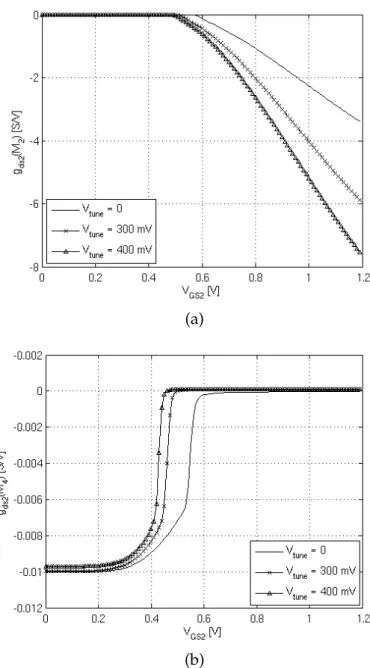
4.5 Coefficientk1as a function ofVGSofM2. . . 56
4.6 Coefficientk2as a function ofVGSofM2. . . 56
4.7 Coefficientk3as a function ofVGSofM2. . . 57
4.8 LNA Gain for three biasing voltages. . . 57
4.9 LNA NF for three biasing voltages. . . 58
5.1 LNA with double feedforward. . . 60
5.2 LNA with local feedforward and feedback. . . 62
5.3 Proposed LNA using double feedback. . . 62
5.4 Gain simulations for the circuit with 1.2 V supply. . . 65
5.5 NF simulations for the circuit with 1.2 V supply. . . 66
5.6 Gain simulations for the circuit with 0.6 V supply. . . 66
5.7 NF simulations for the circuit with 0.6 V supply. . . 67
5.8 SimulatedS11 parameter for the DFB LNA. . . 69
5.9 Simulated gain for the DFB LNA. . . 69
5.10 Simulated NF for the DFB LNA. . . 70
6.1 LNA test setup for evaluation of the integrated prototypes. . . 72
6.2 Layout and die photo of the LNAs with active and passive loads. . . . 73
6.3 LNA test board. . . 74
6.4 Power gain of the LNA with active loads. . . 74
6.5 Power gain of the LNA with passive loads. . . 75
6.6 NF of the LNA with active loads. . . 75
6.7 NF of the LNA with passive loads. . . 76
6.8 Comparison of measured LNA gain with active and passive loads. . . 77
LIST OFFIGURES
6.9 Comparison of measured LNA NF with active and passive loads. . . . 77
6.10 Block diagram of the implemented RF receiver front-end. . . 79
6.11 Die photo and layout: (a) front-end with the LNA with active loads; (b) front-end with DFB LNA. . . 80
6.12 RF front-end test board. . . 81
6.13 Post-layout simulation of S11 parameter for the DFB LNA. . . 81
6.14 Post-layout simulation of gain for the DFB LNA. . . 82
6.15 Post-layout simulation of NF for the DFB LNA. . . 82
6.16 Measureds11 of DFB LNA (receiver B). . . 83
6.17 Measured front-end gain (receiver A and B). . . 83
L
IST OF
T
ABLES
3.1 Summary of the LNAs parameters. . . 44
3.2 Comparison of LNAs tradeoffs. . . 44
4.1 Circuit design values. . . 50
4.2 LNA Performance. . . 57
5.1 Circuit simulations for 1.2 and 0.6 supply voltage. . . 65
5.2 LNA circuit parameters using DFB. . . 67
5.3 Optimized voltage gain (dB) for different topologies. . . 68
5.4 Circuit simulations for different topologies with 1.2V supply. . . 68
6.1 Circuit measurements for active and passive loads considering WMTS biomedical application [3] . . . 76
6.2 Comparison with state-of-the-art LNAs. . . 78
A
CRONYMS
ft transition frequency.
BiCMOS Bipolar CMOS.
CG common-gate.
CMFB common-mode feedback.
CMOS complementary metal oxide semiconductor.
CS common-source.
DFB double feedback.
DFF double feedforward.
DT discrete-time.
DTMOS Dynamic Threshold MOS.
FFB feedforward and feedback.
FoM figure of merit.
GaAs gallium arsenide.
HBT heterojunction bipolar transistor.
IC integrated circuit.
ACRONYMS
ISM industrial, scientific and medical.
LNA low noise amplifier.
MPW multi-project wafer.
NF noise figure.
RF radio frequency.
SDR software-defined radio.
Si silicon.
SiGe silicon-germanium.
SMA sub-miniature version A.
VCO voltage controlled oscillator.
WMTS wireless medical telemetry service.
WSN wireless sensor network.
C
H
A
P
T
E
R
1
I
NTRODUCTION
1.1
Background and Motivation
In the last decades CMOS technology has been continuously subjected to
down-scaling, mainly driven by digital applications in order to increase circuit speed
and density. However, CMOS transistors have been considered slow devices for
RF applications when compared to devices based on III-V compounds, since the
electron saturated velocity is lower in Si [1].
Until recently, high and low frequency integrated circuits (ICs) were treated
separately. The high frequency ICs could only be realized with large areas in more
expensive technologies than standard CMOS, such as GaAs, SiGe, HBT, Bipolar,
and BiCMOS [2]. This reduction of transistors’ channel length lead to an increase
of the transition frequency (ft), defined as the short-circuit unity current gain
frequency, up to hundreds of gigahertz and a reduction of power consumption,
which made a challenge to implement analog radio frequency (RF) functions in
CMOS technology. Furthermore, research efforts have been made to provide more
accurate and compact device models for analog RF CMOS transistors.
The current proliferation of mobile communication systems and wireless sensor
CHAPTER 1. INTRODUCTION
license free industrial, scientific and medical (ISM) and wireless medical telemetry
service (WMTS) bands [3]. Therefore, there is a large demand for devices that have
reduced cost and power consumption, while maintaining a reliable and efficient
performance. The ultimate goal is to integrate the digital and analog RF circuits in
one chip, which is now possible due to the advance of modern CMOS technologies.
Modern fully integrated receiver architectures (e.g. Low-IF and Zero-IF), require
inductorless circuits to achieve their potential low area, low cost, and low power
[4]. The LNA, which is a key block in such receivers, is investigated in this thesis.
Narrowband LNAs use inductors and have very low noise figure, but they
occupy a large area and require a technology with RF options to obtain inductors
with high Q [5]. Wideband LNAs with multiple narrowband inputs have low noise,
but their design is complex and the area and cost are high [6]. RC LNAs are very
simple and inherently wideband, but their conventional realizations have large
noise figure (NF). Recently, wideband LNAs with noise and distortion cancelling,
with passive loads have been proposed, which can have low NF, but have high
power consumption [7].
The mains focus of this PhD work is to investigate low noise amplifiers (LNAs),
which are key blocks of wireless receivers, in particular low area, low power
and low cost LNAs, which are required in ISM and WMTS bands for biomedical
applications. However, a wideband LNA can be used in modern software-defined
radio (SDR) receivers. Simulation and experimental results are provided which
confirm the theoretical analysis.
It is used the LNA architecture employed in [8], with noise and distortion
cancelling, which combines a common-gate (CG) stage and a common-source
(CS) stage. In [8] resistor loads are used in these two stages. In this thesis, the
resistor loads are replaced by MOS transistors, biased in moderate inversion and
operating near the transition between triode and saturation, which allows the
increase of the LNA gain (for the same voltage drop) and minimizes the circuit
NF, without increasing the circuit die area; the active loads allow a supply voltage
reduction, which can lead to a very low power consumption. This adds a new
degree of freedom that allows the use of feedback and feedforward techniques for
1.2. THESIS ORGANIZATION
gain enhancement and noise reduction, with minimum impact in linearity.
Two circuit prototypes have been designed in a standard 130 nm CMOS
technol-ogy to compare the conventional design with resistors [8], and the new
implemen-tation, with active loads. We demonstrate that the proposed design methodology
leads to a gain boost of 3 dB and reduces the NF by 0.5 dB. We also present a very
low area and low cost LNA, with using a double feedback (DFB) technique to boost
the gain and reduce the noise figure. A circuit prototype in a 130 nm standard
CMOS technology at 1.2 V has been designed and simulated to demonstrate the
proposed technique.
Simulation results show a gain of 24 dB and NF below 2.7 dB, with power
dissipation of only 5.4 mW, leading to a figure of merit (FoM) of 3.8 mW.
Measure-ment results of the proposed DFB LNA which is included in a modern receiver
are also presented, proving that the proposed approach leads to a high gain, low
NF circuit, when compared with other state-of-the art approaches.
1.2
Thesis Organization
This thesis is organized in seven chapters, including this introduction.
In Chapter 2, an overview of fundamental concepts for wireless receivers
and LNAs is given. The conventional RF front-end architectures, where the LNA
is included, are presented and the most common LNA topologies are briefly
described. The main performance parameters and definitions relevant for receivers
and in particular for LNAs are also introduced, such as impedance matching, noise
figure, intermodulation products and FoMs.
Chapter 3 gives a review of the state-of-the art LNAs. It is focused on wideband
architectures, which exploit several techniques that offer additional freedom in
LNA design to overcome the trade-off between input matching and NF that is
usually critical in design.
In Chapter 4 an LNA with active loads is investigated. It is shown that this
configuration allows the implementation of an LNA with continuously controllable
CHAPTER 1. INTRODUCTION
is compared with a similar version with resistive loads under the same bias
conditions.
In Chapter 5 two LNA design approaches are introduced, namely double
feedforward (DFF) and DFB . Through the use of local feedback techniques the
gain can be maximized and the overall noise figure is reduced. The DFF LNA is
particularly interesting under low supply voltage, and simulation results show
that it is feasible and can achieve high gain with a supply of 0.6 V. The DFB LNA
offers the best performance among the presented LNA topologies.
In Chapter 6, measurement results are presented. First, the LNAs implemented
with resistors and with active loads are compared. Then the implementation of a
modern RF front-end for low-IF receivers is discussed, where the proposed LNA
is included. For comparison purposes, two versions of the RF front-end were
designed and implemented, one using the LNA with active loads and the other
using the proposed DFB LNA.
Finally, Chapter 7 is devoted to a discussion of the results. Conclusions are
drawn and future work is suggested.
1.3
Original Contributions
The main contributions of this thesis are as follows.
We present a detailed balun LNA with active loads. This circuit is compared
with the traditional design with resistive loads [9]. The active loads allow a
contin-uously controllable gain. A complete theoretical analysis of linearity and noise has
been done regarding the minimization of intermodulation products. The result
this work has been published in [10].
In order to find alternative solutions to achieve higher gain and lower noise
figure for the balun LNA with the new degree of freedom allowed by active loads,
new topologies were investigated exploiting the use of local feedback without
degradation of linearity. Based on this new approach, the following new circuit
designs are proposed:
• A DFF LNA with high gain and under 0.6 V supply operation, with very low
1.3. ORIGINAL CONTRIBUTIONS
power consumption, which is particularly useful for biomedical applications
[11].
• An LNA in which the gain is boosted and the noise figure is reduced by
using a double feedback structure [9].
Finally, measurement results are presented for the proposed LNA with active
loads (without feedback) and for a DFB LNA, both included in a receiver front-end
for biomedical applications (ISM and WMTS). These measurements prove that the
proposed approach using double feedback leads to a high gain, low NF circuit,
when compared with other state-of-the art approaches. This work has lead to a
publication in a special issue of an international journal for RF design techniques
C
H
A
P
T
E
R
2
W
IRELESS
R
ECEIVERS AND
LNA
S
In this chapter, an overview of receiver architectures and of the conventional
low noise amplifiers is made. The basic concepts and definitions used in wireless
systems and main RF performance parameters used in LNAs and RF circuits are
described to provide the background on which this PhD work is based.
2.1
Receiver Architectures
A communication system is composed of a transmitter, a receiver, and a
commu-nication channel, in which, the signal is propagated. On the transmitter side, the
signal containing the information is included in a periodic signal, denominated
carrier, through a process called modulation which consists of the variation of,
at least, one of its characteristics, amplitude, frequency, or phase. The main
func-tion of the receiver is to recover the informafunc-tion contained in the original signal
through a demodulation process.
In a wireless system, the signals are converted to high frequency for
transmis-sion and propagated through the air, and then down-converted to the baseband
for reception. This conversion is necessary for two main reasons: the signals can
carry more information at high frequencies (higher bandwidth) and small size
CHAPTER 2. WIRELESS RECEIVERS AND LNAS
of the signal). Although the communication medium is far from ideal, and the
signal received is usually very weak (of the order of microvolts), and is also
sus-ceptible to interferences from other signals (that can be stronger). Therefore, it is
necessary to eliminate unwanted signals and detect the information contained in
the signal of interest. In the following sections, the main receiver architectures that
are commonly used today are briefly described [4], [13].
2.1.1
Heterodyne Receiver
The heterodyne receiver topology, represented in Fig. 2.1, was proposed by
Arm-strong in 1918 [14] and is one of the most used architectures in wireless
communi-cation systems. The RF signal received by the antenna is filtered by a bandpass
filter, thus minimizing the influence of near interferers, then it is amplified by a
low noise amplifier and down-converted to a lower, intermediate frequency (IF),
through a signal multiplier (mixer), to which the output of a local oscillator (LO) is
applied. At the mixer output there is a bandpass filter at the IF, called the channel
selection filter, which isolates the desired signal from signals in adjacent channels.
The signal demodulation is usually done in the digital domain and, therefore, it is
necessary to include an analog to digital converter (ADC), followed by a digital
signal processor to perform the demodulation process.
Data LNA VCO RF Band-Pass Filter Image Rejection Filter Channel Selection Filter f rf f rf f lo f if DSP ADC
Figure 2.1: Heterodyne Receiver.
The main advantage of this architecture is that the IF is fixed, so the desired
frequency is selected by tunning the LO, making it easier to design the channel
selection filter, which should be very selective, with a high quality factor (Q).
However, a major problem can occur if at the mixer input also exists a signal, called
image signal, with frequency fim = 2flo− fr f, as shown in Fig. 2.2. This signal
2.1. RECEIVER ARCHITECTURES
after the multiplication originates at the mixer output two signals at frequencies
f1 = flo − fr f and f2 = 3flo − fr f, and since f1 coincides with the intermediate
frequency, it overlaps the signal of interest, and it is impossible to separate the two
signals.
f
if frf flo fim f f
if f
if
Figure 2.2: Frequency spectrum showing the image signal.
A filter is necessary before the mixer to reject the image signal (image rejection
filter). Furthermore, the frequency difference between RF and image signals is
2fi f, hence, increasing fi f relaxes the image rejection filter specifications. However, as fi f increases, the channel selection filter must have tighter specifications for
the same bandwidth, because the quality factorQ, which is proportional to the
centre frequency, increases. Filters with a highQare difficult to realize with CMOS
technology, and so there is a trade-off between intermediate frequency and quality
factor. In practice, high performance filters must be realized externally, which
makes on chip full integration impractical.
2.1.2
Homodyne or Zero-IF Receiver
To overcome the difficulty of implementing a fully integrated heterodyne receiver,
another receiver architecture is employed, commonly referred to as homodyne,
direct conversion, or "Zero-IF". In the direct conversion receiver, the RF signal is
converted directly to the baseband by using an LO with the same frequency as the
RF signal, which eliminates the problem of the image rejection; thus, the image
rejection filter is no longer required. Moreover, with the signal of interest in the
baseband, the channel selection filter can be replaced by a low-pass filter which is
CHAPTER 2. WIRELESS RECEIVERS AND LNAS
In Fig. 2.3(a) a simplified direct conversion receiver is represented which is
suitable for double-sideband amplitude modulation (AM) signals, since, after
the down conversion, both sidebands are overlapped in the baseband, carrying
the same information. However, for more sophisticated modulation schemes,
such as frequency modulation (FM) or quadrature phase-shift keying (QPSK),
the sidebands may carry different information, and in order to avoid loss of
information after the down conversion, a quadrature architecture is used as shown
in Fig 2.3(b).
VCO
Low-pass Filter LNA
(a)
LNA
+
VCO90°
I
Q
(b)
Figure 2.3: Homodyne receiver: (a) single receiver (b) quadrature receiver.
Despite its low complexity, this architecture presents some drawbacks,
de-scribed below, that prevent it from being applied in some cases.
DC offsets One problem is related to leakages between the LO port and the LNA
and mixer inputs, when the ports are inadequately isolated, due to substrate and
capacitive coupling. When a leakage signal from the LO appears at the inputs of
LNA and mixer, there is a “self-mixing” effect that originates a DC component at
the mixer output, which can lead to saturation of the following stages. A similar
effect occurs if there is a leakage from the LNA or mixer input to the LO port of
the mixer.
I/Q Mismatch As referred above, with frequency or phase modulation,
quadra-ture signals are required and ideally they should have the same amplitude and
2.1. RECEIVER ARCHITECTURES
a phase difference of 90◦. However, the circuits are not ideal and imbalances
be-tween IandQsignals are expressed as gain and phase errors. The result of this
"I/Q mismatch" is a corruption of the received signal constellation, which would
cause a degradation of the system performance such as an increase of the bit error
rate (BER).
Even order distortion If the LNA has a second order nonlinearity such as
y(t) = a x(t) +b x2(t), and if near the channel of interest there exist two close
interferers,x(t) = A1 cos(ω1t) +A2 cos(ω2t), one of the resulting output terms
isb A1 A2 cos((ω1−ω2)t). This indicates that one of the interferers component
is near the baseband (ω1−ω2), and in the case of an ideal mixer, there is no
problem, because, after multiplication by the LO signal, this component is shifted
to high-frequencies. However, the mixers are not ideal and exhibit some
feed-through directly to the output, so part of the interferer appears at the output at
the baseband, together with the down converted signal, which leads to signal
distortion.
To avoid this problem, differential LNAs and mixers should be employed in
order to eliminate even order harmonics, but this implies more power consumption
and larger circuit area.
Flicker noise Another drawback is the existence of “flicker noise” that is more
significant for low frequencies, specially for MOSFETS. This noise causes signal
degradation if it appears in the baseband, at the mixer output. The flicker noise
subject is further discussed in section 2.2.
In spite of their simplicity, homodyne receivers are impractical for some
ap-plications, although there are techniques to solve some of the above mentioned
CHAPTER 2. WIRELESS RECEIVERS AND LNAS
2.1.3
Low-IF Receiver
The low-IF topology combines the advantages of both types of receivers,
hetero-dyne and homohetero-dyne, by using a mixed approach, i.e, by using a low intermediate
frequency. This relaxes the channel selection filter specifications and
simultane-ously avoids the problems related to direct conversion, in particular the flicker
noise that strongly affects the baseband signal. To overcome the image problem
associated with the heterodyne receiver, a technique to cancel the image signal
is employed in order to avoid the image rejection filter. The image cancellation
is achieved by using quadrature architectures, in which the image is suppressed
after generating a negative replica.
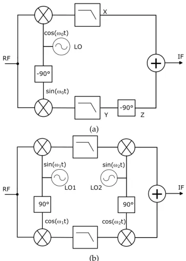
+
cos(w0t)Y sin(w0t)
X
-90°
-90° Z
IF RF
LO
(a)
+
sin(w1t)cos(w1t)
90°
IF RF
sin(w2t)
cos(w2t)
90°
LO1 LO2
(b)
Figure 2.4: Image rejection architectures: (a)Hartley (b)Weaver.
The Hartley [15] architecture shown in Fig. 2.4(a), is one of the alternatives to
cancel the image signal. If at input there is the signal and the corresponding image
2.1. RECEIVER ARCHITECTURES
x(t) = VRF cos(ωRFt) +VIm cos(ωImt), after down conversion and filtering the
resulting signals at X and Y are, respectively:
x(t) = VRF
2 cos((ωRF−ωLO)t) +
VIm
2 cos((ωLO−ωIm)t) (2.1)
y(t) = −VRF
2 sin((ωRF−ωLO)t) +
VIm
2 sin((ωLO−ωIm)t) (2.2)
Sincesin(θ−π2) = −cos(θ), after a−90◦ shift, the signal at Z is,
z(t) = VRF
2 cos((ωRF−ωLO)t)−
VIm
2 cos((ωLO−ωIm)t) (2.3)
Finally, by adding the signals at X and Z, the wanted signal is recovered and the
image is suppressed. The Weaver [16] architecture (Fig. 2.4(b)) produces a similar
result, and the second LO frequency can be chosen to achieve a direct conversion
to the baseband. However, both circuits are susceptible to “I/Q mismatch”, as
referred above, leading to incomplete image rejection.
The low-IF topology allows a flexible compromise between the Zero-IF and
Heterodyne topologies.
2.1.4
Wideband Receiver
The wideband receiver is becoming more popular among the receiver architectures,
due to its flexibility to accommodate multi-band and multi-standard wireless
communications, inspired by software defined radio [17]–[19]. Differently from
conventional RF front-ends, the wideband receiver does not have a filtering stage
after the antenna: therefore, it is fully exposed to the spectrum, which is crowded
of out-of-band interferers and signals from the several wireless standards that
are ubiquitous these days, and consequently, in the absence of filtering, these
interferers have direct impact on the dynamic range and sensitivity of the system.
A strong effort has been made in the development of low cost and low area
wideband receivers, which can be software defined for different bands and
specifi-cations [20]. This type of receivers typically down converts the RF signal to a low
intermediate frequency or directly to the baseband (direct conversion). However,
CHAPTER 2. WIRELESS RECEIVERS AND LNAS
LNA
Q I
S/H
RF
Figure 2.5: Wideband SDR RF front-end receiver [18].
Matching Amplifier Stage
Voltage-Sensing Amplifier Stage
Combining Network
RS
Main Path
Auxiliary Path
Output
Figure 2.6: Noise and distortion cancelling principle [21].
a general architecture of a wideband RF front-end receiver is shown. In the
exam-ple, a discrete-time (DT) passive mixer is used, driven by a multi-phase square
wave oscillator. Passive mixers with hard switching are usually preferred due to
their good linearity, and by combining the sum of properly weighted poly-phase
clock signals, wideband harmonic rejection can be achieved, therefore, relaxing
the filters specifications [18], [21]·
In order to obtain a receiver with low noise and low distortion, a noise and
distortion cancelling principle can be used, which can be done at circuit level (e.g.,
LNA) or in the overall receiver, as shown in Fig. 2.6. Basically the input signal is
divided into two branches: the main signal path and an auxiliary path for sensing,
which are then combined at the output of the LNA or at the Low IF after the
downconversion in the case of a receiver[20].
In this type of receivers the LNA is a critical block, which will set the
perfor-mance of the complete receiver. A wideband LNA is required that can provide
a stable input matching on the entire band of interest, with enough gain not to
compromise the overall linearity, while at the same time the NF must be very low.
2.2. LNA PERFORMANCE PARAMETERS
Thus, the main motivation of this thesis is to design a CMOS wideband LNA,
suitable to be used in wideband receivers for biomedical applications.
2.2
LNA Performance Parameters
2.2.1
Impedance Matching
Lumped circuit analysis assumes that the network’s dimensions are much smaller
than the electromagnetic wavelength, and therefore, the signal propagation over
the network is practically instantaneous. However, for high frequencies the
wave-length tends to be of the same order of the circuit dimensions, and consequently the
circuit paths behave like transmission lines, which require distributed parameter
analysis. When a transmission line is terminated by a loadZL, the voltage
reflec-tion coefficient defines the amplitude of a reflected voltage wave (Vo−) normalized to the incident wave amplitude (Vo+), as follows [22]:
Γ= V
− o Vo+
= ZL−Z0
ZL+Z0
(2.4)
whereZ0is the transmission line characteristic impedance. To achieve the
maxi-mum power transfer to the load, there should be no reflection, i.e,Γ =0, which
only occurs whenZL =Z0, and then the load is matched to the line characteristic
impedance. Usually in RF systems the antenna has a characteristic impedance of
50Ω, so the first block of a receiver must have the input impedance of 50Ω.
2.2.2
Scattering Parameters
At high-frequencies, the usual system characterization used in low frequencies
trough open and short-circuit measurements is more difficult than measuring the
average power, because currents and voltages measurements involve the
magni-tude and phase of the travelling waves [23]. For that reason, at high-frequencies
(when the device length is not negligible with respect to the wavelength) different
CHAPTER 2. WIRELESS RECEIVERS AND LNAS
(S-parameters) relate the power of incident and reflected waves, at n-ports, trough
the scattering matrix,
b1 ... bn =
S11 · · · S1n
... ...
Sn1 · · · Snn
· a1 ... an (2.5)
where,an is the incident power wave at portnandbn corresponds to the reflected
wave. A specific s-parameter is determined as follows,
Sij = bi
aj
ak=0,k6=j
(2.6)
which physically means that an s-parameter gives the ratio between the reflected
wave at portiand the incident wave at port jwhen the other ports are terminated
with a matched load to avoid unwanted reflections. The s-parameters are measured
directly with a network analyser, and allow an accurate network characterization
without knowing in detail the circuit inside the network.
For the particular case of a two-port network (Fig.2.7) the s-parameters are
designated according to their physical meaning [22]:
• S11 - Input reflection coefficient
• S21 - Forward power gain
• S12 - Reverse power gain
• S22 - Output reflection coefficient
2-port
Network
a
1b
1a
2b
2Figure 2.7: Two-Port Network with the incident and reflected waves.
2.2. LNA PERFORMANCE PARAMETERS
In receiver front-ends, the s-parameters are particularly useful in LNA design
due the need of input matching, and are associated with the concept of return
loss. The return loss is a figure of merit for signal reflection and indicates the
fraction of the incident power that is reflected back to the source. LNAs technical
specifications usually include the input return loss, defined as [24],
RL=−20log(|S11|) (2.7)
It is desirable to minimize the reflected power, so more power is transferred to the
load. Typically, designers aim for at least 10 dB return loss, as the requirements for
wireless systems often specify a 10 dB return loss bandwidth [25].
2.2.3
Noise
Noise arises in electronic circuits as a random variable, caused by physical
phe-nomena due to the nature of the materials or by external interferences. Noise is
non deterministic and its instantaneous value can not be foreseen. The presence of
noise in circuits is inevitable, and, therefore, it is important to analyze its impact on
the degradation of signals of interest and develop methods to minimize its effect.
In this section the main noise sources present in CMOS devices are described [6],
[26].
2.2.3.1 Thermal Noise
Thermal noise in circuits is due to the random motion of electrons, causing a
variation of current. The thermal noise power can be expressed as
P =kT∆f (2.8)
whereT is the temperatureT(Kelvin),kis the Boltzmann’s constant and∆f is the
bandwidth of the system. In a resistor, the noise voltage generated is
Vth2 =4kTR∆f (2.9)
and can be modeled by a voltage source in series with the resistor or by a current
CHAPTER 2. WIRELESS RECEIVERS AND LNAS
R f kT In24 f
kTR Vn 4
2
Figure 2.8: Resistor thermal noise models.
MOS transistors also exhibit thermal noise due to the carrier motion through
the channel, and this noise can be represented by a current source in parallel
with the conducting channel (Fig. 2.9). The noise generated when the device is
operating in the triode region is [27]:
I2
n =4kTγgd0∆f (2.10)
wheregd0is the drain-source conductance forVDS =0 andγis the excess noise
factor and has a value of unity. However, the value ofγcan change under different
conditions. For long-channel MOSFET devices operating in saturation [28],
I2
n =4kTγgm∆f (2.11)
is generally assumedγ=2/3 [29]. For short-channel and submicron MOSFETS,γ
has higher values, in a range between 1 and 3 [30].
2
n
I
Figure 2.9: Mosfet thermal noise representation.
For further analysis and notation simplicity it is assumed that ∆f = 1 Hz,
expressing the noise per unit bandwidth.
2.2. LNA PERFORMANCE PARAMETERS
2.2.3.2 Gate Noise
In addition to the intrinsic channel noise of the MOS transistor, there is another
source of the thermal noise due to the distributed gate resistance, which can be
critical as the channel length (L) decreases. This gate resistance is dependent on
the MOS geometry and has two major contributions: the silicide sheet resistance
(resistance of one square), and the contact resistance between the silicide and
polysilicon. According to [31], the gate resistance for a single polysilicon gate
finger, connected on both sides is:
RG = 1 12ρsh
W L +
ρcon
W L (2.12)
where ρsh is the silicide sheet resistance, and ρcon is the silicide-to-polysilicon
contact resistance.
The equivalent noise model can be represented by a lumped resistor, with an
equivalent gate resistance ofRG/3 in series with a voltage noise source (Vn,RG 2)
with a power spectral density of 4kTRG
3 , applied at the gate [32], [33], as shown in
Fig. 2.10
2 , V
n RG 3
RG
Figure 2.10: Equivalent noise model for gate resistance.
The influence of this noise source can be significantly reduced by proper design,
since the effective silicide sheet resistance can be considerably reduced by the use
of several gate fingers [31], [34]. Moreover, the impact of this noise on the circuit
can be minimized if it is much lower than the channel noise, i.e., 4kTRG 3 <<
4kTγ
gm
[32].
2.2.3.3 Flicker Noise
The flicker noise in FETs has origin in a physical phenomenon, somewhat
CHAPTER 2. WIRELESS RECEIVERS AND LNAS
substrate (Si). The random fluctuation of the number of carriers in the channel is
caused by trapping and release of carriers in theSi−SiO2interface. Flicker noise
is proportional to 1/f, so it is dominant at low frequencies. It is represented by a
voltage source in series with the gate with spectral density
Vn f2 = kf
CoxW L fαf (2.13)
where kf is a process dependent constant, which is bias independent and,Cox, W, and L, are the gate oxide capacitance per unit area, width, and length of the
MOSFET, respectively. A cleaner fabrication process results in lower values forkf. For p-channel devices kf is lower than for n-channel devices, and, thus, PMOS
transistors have less flicker noise. The exponent αf is close to unity, and can have values between 0.7 and 1.2 [28]. This type of noise is still subject of study
concerning its origins and modelling.
2.2.3.4 Shot Noise
Shot noise is caused by fluctuation of the current that crosses a potential barrier,
such as in a pn-junction. The diffusion of charge carriers, which is random, causes
the carriers to have different speeds, originating the fluctuation of current around
an average value. The equivalent noise source is given by
I2
ns =2qIDC (2.14)
where q is the electron charge and IDC is the DC current. Shot noise is more
significant in bipolar transistors, because both emmiter and collector currents are
sources of shot noise, since they cross pn-junctions. In MOSFETs, the DC gate
leakage current contributes with shot noise, but it is usually very small and in
most cases it can be neglected.
2.2.3.5 Noise Figure
The noise factor,F, or noise figure, NF, when expressed in dB, is the most common
measure of the noise generated by a circuit (characterized as a 2-port network).
2.2. LNA PERFORMANCE PARAMETERS
The noise factor is defined as the ratio between the total noise power at the 2-port
output and the 2-port output noise power due to the input noise source only:
F = Total output noise power
Output noise due to the source (2.15)
Fig. 2.11 shows a noisy 2-port with power gain A. The noise factor is
F = N2
A2N 1
(2.16)
whereN2is the total noise power available at the output andN1is the noise power
available at the 2-port input.
VS
RS I1 I
2
V1 2-port V2 RL
Figure 2.11: Noisy 2-port with gainA
If the ports are adapted and a power signalS1is applied from generator, then
by the maximum power transfer theorem, the signal power is transferred entirely
to the 2-port, and so is the signal powerS2 from the 2-port output to the load
resistorRL. The power gain is
A2 = S2
S1 (2.17)
so,
F = N2
A2N 1 = S1 N1 S2 N2
= (S/N)i (S/N)o
(2.18)
The last equation relates the noise factor with the signal to noise ratios at the
input and output of the 2-port, which shows the degradation of the signal to
noise ratio due to the noise introduced by the 2-port. When no additional noise is
introduced by the 2-port,F =1.
2.2.4
Linearity
The performance related to linearity can be characterized by the 1 dB compression
point and by the 2nd and 3rd-order intermodulation products. These parameters
CHAPTER 2. WIRELESS RECEIVERS AND LNAS
A linear system when excited by an input signal generates an output signal
proportional to the input. Most devices have a non-linear characteristic, and if
they are memoryless and time invariant, then their operation can be represented
by a Taylor series, i.e,
y= a0+a1x+. . .+anxn (2.19)
The terms used to represent these devices depends on the type of non-linearity,
being its representation more accurate if more terms are used.
2.2.4.1 Harmonics and Intermodulation Products
Nonlinear devices generate harmonics. A nonlinear device characterized by a
third-order polynomial is usually a good approximation, that simplifies the calculations.
If the input signal is sinusoidal,
vi(t) = Vmcos(ωft) (2.20)
the output is
y(t) = a0+a1Vmcos(ωft) +a2Vm2cos2(ωft) +a3Vm3cos3(ωft) (2.21)
or
y(t) = a0+ a2V 2 m
2
| {z } DC component
+
a1Vm+3a3V 3 m
4
cos(ωft)
| {z }
1stHarmonic(f undamental)
+a2Vm2
2 cos(2ωft)
| {z }
2ndHarmonic
+a3Vm3
4 cos(3ωft)
| {z }
3rdHarmonic
(2.22)
A nonlinearity of orderngeneratesnharmonics with multiples of the fundamental
frequency (nωf). The even order coefficients affect the DC component, whereas the odd order coefficients have impact on the fundamental frequency amplitude.
If, instead of applying a single sinusoidal signal at the non-linear device input,
two signals are applied with different frequencies:
vi(t) =V1cos(ω1t) +V2cos(ω2t) (2.23)
2.2. LNA PERFORMANCE PARAMETERS
intermodulation products are generated at the output, given by:
y(t) =a0+a1(V1cos(ω1t) +V2cos(ω2t))+
a2
V12
2 (1+cos(2ω1t)) + V22
2 (1+cos(2ω2t))+ V1V2(cos((ω1+ω2)t) +cos((ω1−ω2)t))
+ a3 3
4V13+32V1V22
cos(ω1t) + 34V23+32V2V12
cos(ω2t)+ 3
4V12V2(cos((2ω1+ω2)t) +cos((2ω1−ω2)t))+ 3
4V22V1(cos((2ω2+ω1)t) +cos((2ω2−ω1)t))+ 3
4V13cos(3ω1t) +34V23cos(3ω2t)
(2.24)
In addiction to harmonics, intermodulation products appear at frequenciesnω1±
mω2. Fig. 2.12 illustrates the intermodulation products for a particular case of a
nonlinearity of order 3.
f2 f1
2f2-f1
f f2-f1
2f1-f2
2f1 f1+f22f2 ω2-ω1
2ω1-ω2
ω2
ω1
2ω2-ω1 2ω
1ω1+ω22ω2
ω
Figure 2.12: Frequency spectrum showing the intermodulation products of a nonlinear device of order 3.
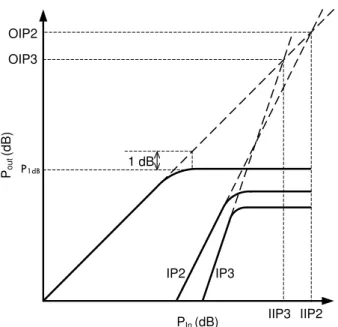
2.2.4.2 1 dB Compression Point
The 1 dB compression point is a linearity measure of a circuit and is defined as
the output signal power that corresponds to a difference of 1 dB from the ideal
(linear) circuit, as shown in Fig. 2.13. At that point, the compression is reached
which consequently degrades the signal.
2.2.4.3 Intercept Points
The nth order intercept point (IPn) is defined as the point at which the curves
CHAPTER 2. WIRELESS RECEIVERS AND LNAS
(dB)
Ideal
Real Pout
(dB) Pin P1dB_i
P1dB_o 1 dB
Figure 2.13: Definition of 1 dB compression point.
product would intercept if they were linear (asymptotically extrapolated), i.e, when
the amplitude of the fundamental frequency would be equal to the amplitude of
thenthintermodulation product. The specifications for intercept points are often
input-referred I IPn, but can also be output-referredOIPn, as illustrated in Fig.
2.14. The most commonly intercept points used to characterize a LNA are IP2
and IP3. A practical rule that is employed in most radio frequency amplifiers is
that the 1 dB compression point falls at least 10 dB below the third order intercept
point.
PIn (dB)
1 dB
Po
u
t
(d
B
)
P1dB
OIP3
IIP2 IP3
IIP3 OIP2
IP2
Figure 2.14: Intercept points.
2.3. BASIC LNA CIRCUITS
2.2.5
Figures of Merit for LNAs
In the literature it is common to find a variety of LNA designs, optimized for
different parameters such as gain, noise figure, linearity, and power consumption.
Even for similar topologies, the results can be quite different, depending on the
optimization purpose. To compare these different designs, usually the most
impor-tant parameters are included into a formula called figure of merit (FoM) in order
to determine which design is more efficient. A popular FoM (2.25) is related the
noise and gain performances, and is normalized to the power consumption [35].
FoM1[mW−1] = Gain
(F−1)·PDC[mW] (2.25)
However, nothing can be concluded about the performance regarding the other
parameters. In (2.26) a more complete FoM is presented, proposed in [36], that
includes I IP3 and the frequency of operation fC. This FoM is suitable for
narrow-band LNAs only, since the narrow-bandwidth is not considered.
FoM2[−] = Gain(·IIP3[mW]· fc[GHz]
F−1)·PDC[mW] (2.26)
In order to have a fair comparison between wideband and narrowband LNAs , in
[37] a FoM is proposed that includes the bandwidth and area, as follows:
FoM3[dB] =20 log
Gain·IIP3[mW]·BW[GHz] (F−1)·PDC[mW]·A[mm2]
(2.27)
2.3
Basic LNA Circuits
In this section, typical LNA specifications and LNA circuits are discussed.
The LNA, is typically the first amplifying stage. The LNA input impedance
should match the antenna characteristic impedance to maximize the power transfer.
The LNA should provide enough gain in order to minimize the overall influence
of noise contribution from the subsequent stages, but the gain should not be too
high, since large interferer signals that may have not been properly filtered at the
input can saturate the following stage (e.g. mixer); in practice, a reasonable range
CHAPTER 2. WIRELESS RECEIVERS AND LNAS
The noise factor should be the lowest possible to minimize the noise in the
system, since the noise contribution of the first stage in a cascaded system is
dominant, and besides the noise figure specifications could differ for different
applications, a reasonable value usually adopted for the noise figure is below 3 dB.
As to LNA circuits, there are four basic approaches according to the input
impedance matching, as described in the following [38].
2.3.1
Common-Source LNA with Inductive Degeneration
The CS LNA with inductive degeneration is one of the most used topologies to
design a narrowband LNA, because it allows low noise figure, high gain, and easy
input matching. The CS LNA shown in Fig. 2.15 is intrinsically narrowband since
RL
Ls
Lg
Zin
Figure 2.15: Common-Source LNA with inductive degeneration.
its input impedance is
Zin=s(Lg+Ls) + 1 sCgs
+ gm
Cgs
Ls (2.28)
and the inductances Ls andLgare chosen to resonate with the device capacitance
Cgsat the frequency of operation
ω0 = q 1
(Lg+Ls)Cgs
(2.29)
This eliminates the imaginary part of Zin and the term Cgm
gsLs is set to 50
Ω.
The inductanceLggives a degree of freedom in the LNA design, since the gain is
proportional togm. The use of inductors, which are ideally noiseless, allow this
topology to have one of the best noise performances, but it increases significantly
the die area of the LNA. A major drawback is that RF options (thick metal layer)
2.3. BASIC LNA CIRCUITS
needed to design high Q inductors , and the large die area, increase the production
cost.
2.3.2
Common-Source LNA with Resistive Input Matching
The simplest way to obtain a stable wideband input impedance is to use resistive
input matching. The CS stage, shown in Fig. 2.16, has a resistor is in parallel with
the amplifier input. However, this resistor introduces a significant amount of noise.
ZL
Rin
Zin
Figure 2.16: Common-Source stage with resistive input matching.
Assuming that the amplifier has an available power gainApand a noise power
at the outputPn, due to internal sources only, if the source has an impedance RS,
the noise factor can be expressed by:
F = Total output noise
Total output noise due to input source
= 4kTRSAp+4kTRinAp+Pn
4KTRSAp =2+
Pn
4KTRSAp (2.30)
which establishes a minimum noise figure of 3 dB, which is a high value for some
applications.
2.3.3
Common-Gate LNA
The common-gate topology (Fig. 2.17) has an intrinsic wideband response, which
is one of the reasons why it is widely used to implement LNAs. In a first order
anal-ysis, its input impedance is approximately gm1 , and gm can be easily dimensioned
CHAPTER 2. WIRELESS RECEIVERS AND LNAS
ZL
Zin
Vbias
Figure 2.17: Common-Gate LNA.
To estimate the lower bound of the noise factor, only the transistor thermal
noise is considered. If it is referred to the input, we obtain [38]:
F =1+γgd0RS =1+γ
αgmRS (2.31)
whereα ≈ ggm
d0. For long channel devices, the noise excess factorγ
1is 2
3 and the
short-channel effects can be neglected (α = 1) [29], [30]. For input matching,
gmRS =1. Thus, the minimum noise factor is aboutF= 53, which corresponds a
noise figure of 2.2 dB.
The CG-LNA has a disadvantage: sincegm is imposed by the matching
condi-tion, the gain is only dependent on the loadZL. IncreasingZL increases the gain,
but also increases the noise. This limits the gain that it is possible to achieve. In
practice, the CG-LNA has typical noise figure values above 3 dB.
2.3.4
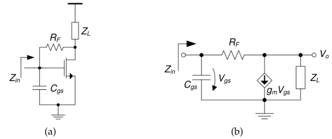
LNA with resistive shunt feedback
The wideband LNA represented in Fig. 2.18(a) uses the feedback resistorRF. Using
the incremental model (Fig. 2.18(b)), the input impedance is:
Zin = RF+ZL
sCgs(RF+ZL) +1+gmZL
=
1
sCgs//
RF+ZL
1+gmZL
(2.32)
which depends on many parameters, so, for the sake of simplicity, some
assump-tions will be made. For frequencies such thatCgs is negligible, the gate is seen as a
high impedance, and assuming thatZL >>RF the input impedance simplifies to
1/gm.
1This value is often empirically determined and can be higher for short channel devices,
between 1 and 3.
2.3. BASIC LNA CIRCUITS ZL Cgs Zin RF (a) ZL gmVgs
Vo RF Cgs Zin Vgs (b)
Figure 2.18: LNA with resistive shunt feedback: (a) schematic (b) small signals model for low and medium frequencies.
Using a similar analysis for low frequencies, the gain is:
Av= (1−gmRF)ZL RF+ZL
(2.33)
and if the loadZL is high andgmRF >>1, the gain is simplified to:
Av ≈ −gmRF (2.34)
This approximation is useful when considering the noise factor, that is found to be
[39]:
F=1+RF
RS
1+gmRS
1−gmRF 2
+ 1
RSZL
RF+RS
1−gmRF 2
+ γgm
αRS
RF+RS
1−gmRF 2
(2.35)
At first sight, by increasing the term gmRF, the noise factor is reduced and the
gain is enhanced, as intended. According to the previous assumptions for gain
and noise optimization,gm is set by the input matching condition, andRF must be
increased. However if the loadZL becomes comparable toRF, then the previous
assumptions are no longer valid. Thus,gmandRFhave to be carefully dimensioned
C
H
A
P
T
E
R
3
S
TATE
-
OF
-
THE ART
W
IDEBAND
LNA
S
Recently there has been a proliferation of wireless communication standards that
cover a wide range of the spectrum, from tens of MHz up to several GHz. This has
led to the development of multi-standard radio architectures capable of handling
the stringent specifications of the standards. With this in mind, two approaches to
multi-standard RF front-ends are possible, one using several dedicated
narrow-band LNAs covering the specific target narrow-bands and the other by employing a single
wideband LNA. The first approach has the advantage that narrowband LNAs are
known to achieve better performance, particularly very low noise figures, but it
increases the circuit complexity and the production cost is high, due to the large
area occupied. Wideband LNAs have larger noise figure than narrowband LNAs,
but are simpler and typically have lower power consumption and cost. Therefore,
their use have become very popular which motivated much of the research effort
in wideband LNAs, in order to obtain reasonable noise figures.