Abstract— This paper presents a design and simulation of a low
noise amplifiers (LNA) with all passives elements embedded on low temperature co-fired ceramic (LTCC) substrate. Simulation results in ANSYS Designer and CST Studio Suite reveal that the proposed LNA has a flat-gain of 23.34 dB from 300 to 500 MHz, a noise figure below 0.73 dB and a compact size of 16.7 mm x 8.5 mm.
Index Terms— Embedded Passives, LNA, LTCC, UHF.
I. INTRODUCTION
Low temperature co-fired ceramic (LTCC) technology presents flexibility and high integration
capability. It is commonly used in system-in-package (SiP) [1] and system-on-package (SoP) [2].
Passives elements like capacitors, inductors and resistors can be embedded in the substrate. Therefore
it provides a more compact module size as well as reduces the cost of discrete components and their
assembly time. Consequently, LTCC is widely used in microwave and radio frequency (RF) front-end
module (FEM) [3].
The ultra-high frequency (UHF) ranges from 300 to 1000 MHz for radar nomenclature and up to
3000 MHz for international telecommunications union (ITU) nomenclature [4]. It operates in
line-of-sight (LOS) and ground-bounce with applications in broadcasting, navigation systems and radar.
Furthermore, circuits in UHF are an ideal choice for ground-to-air communications [5].
High-performance receivers require low noise amplifiers (LNA) at the input to optimize noise
figure (NF) [6]. Thus, in this paper a LNA with low NF below 0.8 dB and high gain above 23 dB, for
a output power of 0 dBm (1 mW), using a commercial low cost enhancement-mode pseudomorphic
high-electron-mobility transistor (E-PHEMT) SAV-581+ with fully integrated LTCC passives
requiring no additional components is designed for UHF (300-500 MHz). By simulation, it is
expected lower NF, higher gain and smaller size than others LNA designed in printed circuit board
A flat
-
gain LNA based on LTCC technology at
UHF (300
-
500 MHz)
Rafael R. Heymann1, Juan P. Pantoja1, Leonardo L. Bravo Roger2, Luciano Prado de Oliveira1, Edson C dos Reis3, João R. Moreira Neto3, Hugo E. Hernandez-Figueroa1
1
Department of Communications, School of Electrical and Computer Engineering, University of Campinas - UNICAMP, 13083-852, Campinas-SP, Brazil
2
School of Technology, University of Campinas - UNICAMP, 13484-332, Campinas-SP, Brazil 3
Bradar-Embraer Defesa & Segurança, 13080-010, Campinas-SP, Brazil
transistor S-parameters, next it is drawn and simulated the passives elements and the board layout.
The circuit design is simulated in ANSYS Designer whereas the 3D passives elements and the LNA
layout are simulated in CST Studio Suite. In order to verify the design methodology the schematic
circuit and the layout are compared.
II. METHODOLOGY AND DESIGN
The design relays on a common source transistor with negative feedback configuration where a
feedback resistance is used to minimize the dc current and voltage variations in the bias circuit. Under
small-signal operation, the LNA is linear and, consequently, S-parameters can be used to characterize
it [7]. The approach starts by the stabilization of the transistor adding resistances on the gate and on
the drain which are the input and output of the active device, respectively. These resistances are the
same used to the transistor’s biasing. Then it is found the impedance that the active device sees at the
input because the optimum impedance for lower noise is not equal to the conjugate of input
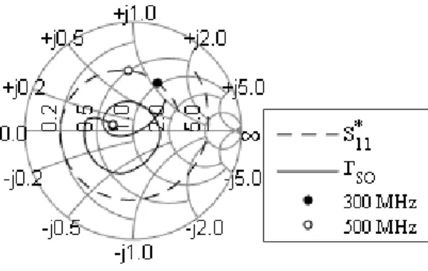
impedance as can be seen in Fig. 1, in other words, there is a tradeoff between low noise and input
matching.
Fig. 1. Smith chart of optimum, ΓSO, and source (input conjugate), S11*, impedances of the transistor with a feedback circuit.
The use of transmission line in the range of frequency from 300 MHz to 500 MHz is unfeasible due
to the long wavelength. Thus, the match impedance networks are built by lumped elements by the Q
matching technique with L-C sections [8]. The 50 Ω input circuit terminal is transformed in that
tradeoff impedance. After that the same technique is used to match the 50 Ω output circuit terminal to
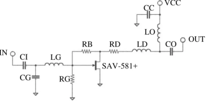
the active device output impedance. Fig. 2 shows the circuit schematic supplied by a 5 V VCC that
ensures the polarization current of 40 mA through the transistor with a 3 V between drain and source
and deliveries a power supply of 200 mW to the circuit, where RB is the feedback resistance, RG is
the input stabilization resistance, RD is the output stabilization resistance, CI, CG and LG are input
matching elements, LD, LO and CO are output matching elements and the capacitor CC is a
Fig. 2. LNA circuit schematic.
The passives elements are designed by compact architectures in a commercial 20-layer LTCC
technology utilizing standard unfired thickness 114 µm DuPont 951PT tapes. The tapes have
dielectric constant 7.8, loss tangent 0.006 at 3 GHz and a shrinkage post fired of 12.7% on x-y axis
and 15% on z axis. The metallization is a 9 µm DuPont and the resistances are DuPont CF011, CF021
and CF031 which 10 ohms/sq, 100 ohms/sq and 1000 ohms/sq sheet resistances, respectively.
The circular helical inductors are used because they have higher Q and self-resonant frequency
(SRF) values as compared to 2-D standard inductors and the circular geometry has the best electrical
performance [9]. Fig. 3(a) shows a 9.5 turn helical inductor. The helical type has only half a turn on
each layer which reduces the coupling capacitance by increasing the distance between the top turns
and the underlying turns, thereby preventing considerable degradation in SRF [10]. Table I shows the
behavior of inductance value, Q and resistance of the coil at 400 MHz in function of its inner radius
and the total area of the element.
TABLE I. INDUCTOR PARAMETERS
Inductance [nH] Q Resistance [Ω] Inner radius [µm] Area [mm2]
15.9 342.8 0.12 251.5 0.835
17.6 341.5 0.13 268.5 0.900
55.1 299.3 0.46 532.5 2.207
It is possible to find a commercial 16 nH inductor 0402 (1 mm x 0.55 mm) but its Q is less than 50
in the desired band, very lower than the 15.9 nH based on LTCC technology shown in Table I which
Q is 342.8. This difference could modify the matching network response and add some loss in the
amplifier.
IN
OUT VCC
SAV-581+
RB RD
RG LG
LD LO
CG CI
Capacitor are conventionally built using metal-insulate-metal (MIM) element that is a dielectric
layer sandwiched between two square plates. Since the capacitance is proportional to the plate areas,
high capacitance requires large areas. Alternatively, vertically-interdigitated capacitor (VIC) works
like a parallel combination of pairs of plates that increase the capacitance because it increases the
effective area as well as it reduces the plate separation. Therefore a same capacitance of a MIM can be
obtained with a dramatically smaller size VIC. Thus, VIC is a suitable architecture to realize an
extremely compact capacitor [11]. Fig. 3(b) illustrates the concept of a 20-layer VIC. Fixed this
structure, the capacitance is defined by the plate’s area.
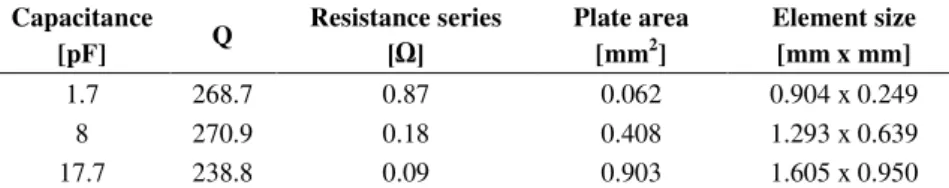
Table II shows the capacitance value, Q factor, resistance series, the plate area and the element size
for each required LNA capacitance. It is possible to find a high-Q capacitor 0.4 mm x 0.2 mm. Thus,
the benefits of using LTCC technology in this project are: flexibility of values and no need to have a
stock of components, neither to buy any passive element.
TABLE II. CAPACITOR PARAMETERS
Capacitance
[pF] Q
Resistance series
[Ω]
Plate area [mm2]
Element size [mm x mm]
1.7 268.7 0.87 0.062 0.904 x 0.249
8 270.9 0.18 0.408 1.293 x 0.639
17.7 238.8 0.09 0.903 1.605 x 0.950
The CC capacitor is not shown in Table II because it works like a short circuit to ground for RF. It
has a SRF in the operate band.
The capacitor’s size can be reduced by using ESL ElectroScience tapes with a dielectric constant as
high as 16 like 41060 or using capacitor dielectric pastes with 50-250 dielectric constant for 4160-N
Series. Smaller inductor could be done using ferrite tapes with 50 (40010), 200 (40011) or 500
(40012) magnetic permeability.
The resistors are designed setting the length and width of a paste according to its sheet resistance.
The resistance is proportional to squares number between the terminals. Table III shows the resistance
in function of the sheet resistance and the square numbers. There are many combinations of
dimension resulting in the same resistance as long as the ratio between the length and the width
remains constant. Thus, the dimensions are calculated based on thermal conduction of the substrate so
that the temperature not to exceed 20oC as in (1).
∆� = � ���= � ��ℎ (1)
Where ∆T is the temperature difference (in oC) between the resistor and the back side of the substrate
due to Pdc (in W) power dissipated in the resistor, RTH is the thermal resistance, A (in m2) is the
equivalent area of the resistor, h (in m) is the thickness, and K (in W/m-°C) is the thermal
TABLE III. RESISTANCE DIMENSIONS
Resistance [Ω] Dimension [mm x mm] Square numbers Sheet resistance [Ω/sq]
49 3.42 x 0.699 4.89 10
574 1.565 x 0.272 5.75 100
3640 1.988 x 0.545 3.65 1000
The LNA layout with a size of 16.7 mm x 8.5 mm including all lumped elements embedded and the
E-PHEMT SAV-581+ land pattern is shown in Fig. 4.
Fig. 4. LNA Layout.
III. RESULTS AND DISCUSSION
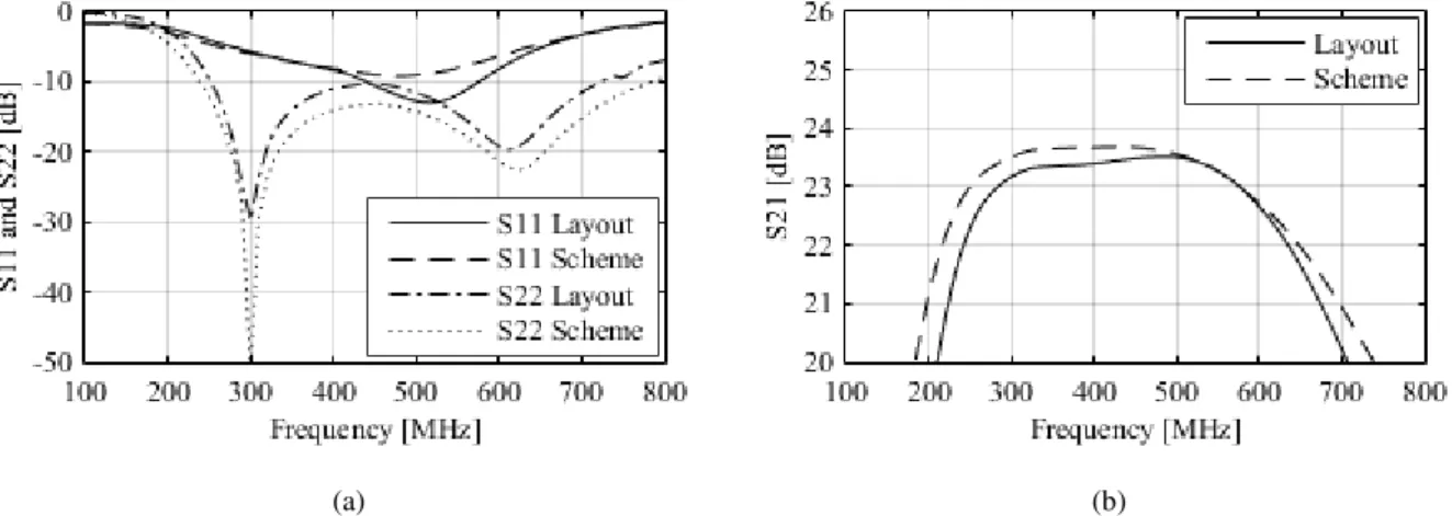
The circuit input (IN) and the output (OUT) in Fig. 4 correspond to 50 Ω ports 1 and 2,
respectively. Fig. 5(a) shows the layout and schematic S11 and S22. Due to tradeoff between the NF
and the input matching, the S11 is slightly higher than -10 dB in the lower band. However, the output
S22 is as low as -10.31 dB for the layout simulation and -13.16 dB for the schematic simulation at 450
MHz. Both simulations match reasonably well.
The S21 is shown in Fig. 5(b), which the schematic value ranges from 23.51 to 23.68 dB and the
layout value ranges from 23.17 to 23.51 dB that means a 0.34 dB variation. Thus the LNA has a
flat-gain around 23.34 dB.
(a) (b)
Fig. 5. Layout vs schematic S-Parameters in dB: (a) S11 and S22 and (b) S21.
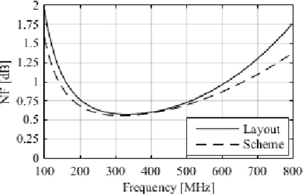
Fig. 6 shows the layout and schematic NF revealing optimum values of 0.5705 at 330 MHz and
0.5543 at 320 MHz, respectively. However, NF increases up to 0.7241 dB in layout simulation and
VCC
IN
OUT
SAV-581+
CC
RD RG
RB
CO LD LO
CG CI
Fig. 6. Layout vs schematic NF in dB.
The project requires low NF and high gain from 300 to 500 MHz. Table IV compares the project
requirements with other LNA designs operating at the same band using a packaged transistor. The
simulation shows this work has the highest gain, lowest NF and smaller size for the operation band.
Photos of two LNA fabricated in a RO4003 PCB in [12] using a transistor which package is like the
SAV-581+ show boards size bigger than this work. In [13], the designed LNA in a FR-4 substrate is
larger than a coin with 25 mm diameter, which has more than three times the area of this work. The
substrate in [14] and [15] are also FR-4.
TABLE IV. LNA DESIGNS
Frequency [MHz] Gain [dB] NF [dB] Dimension [mm x mm] References
136-941 12 1.5 - [12]
136-941 17.3 1.03 - [12]
30-1500 16 1.2 Bigger than 25 x 25 [13]
360-460 23.7 1.5 60 x 32 [14]
50-1000 22-23 2.29 21 x 17 [15]
300-500 23.34 0.73 16.7 x 8.5 This work
IV. CONCLUSION
In this paper it was designed and simulated a 16.7 mm x 8.5 mm LNA operated by a 5V supply that
deliveries about 200 mW to the circuit with 23.34 dB flat-gain, for an output power of 1 mW, and NF
better than 0.73 dB from 300 to 500 MHz using all passives elements embedded on substrate based on
LTCC technology. It was compared the LNA layout simulation with the schematic simulation using
ideal passives elements. The NF difference was lower than 0.032 dB while S21 differs in less than
0.34 dB showing an acceptable agreement between the two simulations. In addition, the embedded
reactive elements have high-Q resulting in low loss. There is only the transistor to be mounted that
reduces cost and assembling time.
Comparing with other works at the same operated band, the simulation of this design has higher
gain, smaller NF and more compact size.
REFERENCES
[2] J. J. Lee, D. Y. Jung, K. C. Eun, I. Y. Oh, and C. S. Park, “A low power CMOS single-chip receiver and system-on-package for 60GHz mobile applications,” in IEEE International Symposium on Radio-Frequency Integration Technology (RFIT)., 2009, pp. 24–27.
[3] B. C. Ham, D. H. Kim, J. M. Yook, J. I. Ryu, J. C. Kim, J. C. Park, Y. C. Park, and D. Kim, “A GPS/BT/WiFi triple-mode RF FEM using Si- and LTCC-based embedded technologies,” in IEEE Microwave Symposium Digest (MTT), 2012, pp. 1–3.
[4] “IEEE Standard Letter Designations for Radar-Frequency Bands,” IEEE Std 521-2002 Revis. IEEE Std 521-1984, pp. 1–3, 2003.
[5] Radio Communications in the Digital Age: VHF/UHF technology, vol. 2. Harris, 2000. [6] P. H. Young, Técnicas de Comunicação Eletrônica, Edição: 5. Pearson, 2006.
[7] R. Gilmore and L. Besser, Practical RF Circuit Design for Modern Wireless Systems, vol. 2. Artech House, 2003. [8] L. Besser and R. Gilmore, Practical RF Circuit Design for Modern Wireless Systems, vol. 1. Artech House, 2002. [9] I. J. Bahl, Lumped Elements for RF and Microwave Circuits. Artech House, 2003.
[10] A. Sutono, A. Pham, J. Laskar, and W. R. Smith, “Development of three dimensional ceramic-based MCM inductors for hybrid RF/microwave applications,” in IEEE Radio Frequency Integrated Circuits (RFIC) Symposium, 1999, pp. 175–178.
[11] A. Sutono, D. Heo, Y.-J. Chen, and J. Laskar, “High-Q LTCC-based passive library for wireless system-on-package (SOP) module development,” IEEE Trans. Microw. Theory Tech., vol. 49, no. 10, pp. 1715–1724, Oct. 2001.
[12] A. F. Osman, N. Mohd Noh, M. T. Mustaffa, and A. Abd Manaf, “Comparison of wideband LNA designs for SDR applications,” in 2nd International Conference on Electronic Design (ICED), 2014, pp. 515–520.
[13] L. Wu and M. Yu, “A wideband low-noise-amplifier with compact size and improved bandwidth,” in International Conference on Microwave and Millimeter Wave Technology (ICMMT), 2010, pp. 653–655.
[14] V. Doki, S. Nandanwar, and J. Thakkar, “Balanced Amplifier Technique for LNA in UHF Band,” in Fifth International Conference on Communication Systems and Network Technologies (CSNT), 2015, pp. 24–27.