School of Technology and Architecture
Design of Adaptive Analog Filters for
Magnetic Front-End Read Channels
Nuno Miguel de Figueiredo Garrido
Dissertation presented in partial fulfillment of the Requirements for the Degree of Doctor of Science and Information Technologies
Supervisor: Prof. Doutor Augusto Afonso de Albuquerque Co-Supervisor: Prof. Doutor Francisco António Bucho Cercas
v
”Era”
–a set of years, which is counted from a particular event or named
after an important development: compare Epoch
...The computer euphoria of modern times is self-evident. The computer has invaded the world, and will soon outnumber mankind. It has entered our quotidian lives, everywhere and inevitably, moreover computer assisted work is becoming the only form of work. Therefore it is natural that many call this the computer era.
Many have taken it as their subject of study, this work will be focused on the information storage process, namely on magnetic hard disk drives.
vii
Sumário
Esta tese estuda o projecto e o comportamento de filtros em tempo contínuo de muito-alta-frequência. A motivação deste trabalho foi a investigação de soluções de fil-tragem para canais de leitura em sistemas de gravação e reprodução de dados em suporte magnético, com custos e consumo (tamanho total inferior a 1 mm2 e consumo inferior a
1mW/polo), inferiores aos circuitos existentes. Nesse sentido, tal como foi feito neste trabalho, o rápido desenvolvimento das tecnologias de microelectrónica suscitou esforços muito significativos a nível mundial com o objectivo de se investigarem novas técnicas de realização de filtros em circuito integrado monolítico, especialmente em tecnologia CMOS (Complementary Metal Oxide Semiconductor). Apresenta-se um estudo compa-rativo a diversos níveis hierárquicos do projecto, que conduziu à realização e caracteriza-ção de soluções com as características desejadas.
Num primeiro nível, este estudo aborda a questão conceptual da gravação e trans-missão de sinal bem como a escolha de bons modelos matemáticos para o tratamento da informação e a minimização de erro inerente às aproximações na conformidade aos prin-cípios físicos dos dispositivos caracterizados.
O trabalho principal da tese é focado nos níveis hierárquicos da arquitectura do canal de leitura e da realização em circuito integrado do seu bloco principal – o bloco de filtragem. Ao nível da arquitectura do canal de leitura, apresenta-se um estudo alargado sobre as metodologias existentes de adaptação de sinal e recuperação de dados em suporte magnético. Este desígnio aparece no âmbito da proposta de uma solução de baixo custo, baixo consumo, baixa tensão de alimentação e baixa complexidade, alicerçada em tecno-logia digital CMOS, para a realização de um sistema DFE (Decision Feedback
Equaliza-tion) com base na igualização de sinal utilizando filtros integrados analógicos em tempo
contínuo.
Ao nível do projecto de realização do bloco de filtragem e das técnicas de imple-mentação de filtros e dos seus blocos constituintes em circuito integrado, concluiu-se que a técnica baseada em circuitos de transcondutância e condensadores, também conhecida
viii
como filtros gm-C (ou transcondutância-C), é a mais adequada para a realização de filtros adaptativos em muito-alta-frequência. Definiram-se neste nível hierárquico mais baixo, dois subníveis de aprofundamento do estudo no âmbito desta tese, nomeadamente: a pes-quisa e análise de estruturas ideais no projecto de filtros recorrendo a representações no espaço de estados; e, o estudo de técnicas de realização em tecnologia digital CMOS de circuitos de transcondutância para a implementação de filtros integrados analógicos em tempo contínuo.
Na sequência deste estudo, apresentam-se e comparam-se duas estruturas de filtros no espaço de estados, correspondentes a duas soluções alternativas para a realização de um igualador adaptativo realizado por um filtro contínuo passa-tudo de terceira ordem, para utilização num canal de leitura de dados em suporte magnético.
Como parte constituinte destes filtros, apresenta-se uma técnica de realização de circuitos de transcondutância, e de realização de condensadores lineares usando matrizes de transístores MOSFET para processamento de sinal em muito-alta-frequência realizada em circuito integrado usando tecnologia digital CMOS submicrométrica. Apresentam-se métodos de adaptação automática capazes de compensar os erros face aos valores nomi-nais dos componentes, devidos às tolerâncias inerentes ao processo de fabrico, para os quais apresentamos os resultados de simulação e de medição experimental obtidos.
Na sequência deste estudo, resultou igualmente a apresentação de um circuito pas-sível de constituir uma solução para o controlo de posicionamento da cabeça de leitura em sistemas de gravação/reprodução de dados em suporte magnético. O bloco proposto é um filtro adaptativo de primeira ordem, com base nos mesmos circuitos de transcondu-tância e técnicas de igualação propostos e utilizados na implementação do filtro adapta-tivo de igualação do canal de leitura.
Este bloco de filtragem foi projectado e incluído num circuito integrado (Jaguar) de controlo de posicionamento da cabeça de leitura realizado para a empresa ATMEL em Colorado Springs, e incluído num produto comercial em parceria com uma empresa es-cocesa utilizado em discos rígidos amovíveis.
ix
Palavras-chave: filtros contínuos adaptativos, comparação de estruturas de filtros, igualação de sinal, tecnologia digital CMOS, processamento de sinal em corrente, circui-tos de transcondutância CMOS, baixo consumo, muito-alta-frequência, área reduzida, baixo custo, baixa complexidade.
xi
Abstract
This thesis studies the design and behavior of continuous-time very-high-frequency filters. The motivation of this work was the search for filtering solutions for the read-channel in recording and reproduction of data on magnetic media systems, with costs and consumption (total size less than 1 mm2 and consumption under 1mW/pole), lower than
the available circuits. Accordingly, as was done in this work, the rapid development of microelectronics technology raised very significant efforts worldwide in order to investi-gate new techniques for implementing such filters in monolithic integrated circuit, espe-cially in CMOS technology (Complementary Metal Oxide Semiconductor). We present a comparative study on different hierarchical levels of the project, which led to the reali-zation and characterireali-zation of solutions with the desired characteristics.
In the first level, this study addresses the conceptual question of recording and transmission of signal and the choice of good mathematical models for the processing of information and minimization of error inherent in the approaches and in accordance with the principles of the characterized physical devices.
The main work of this thesis is focused on the hierarchical levels of the architecture of the read channel and the integrated circuit implementation of its main block - the fil-tering block. At the architecture level of the read channel this work presents a compre-hensive study on existing methodologies of adaptation and signal recovery of data on magnetic media. This project appears in the sequence of the proposed solution for a low-cost, low consumption, low voltage, low complexity, using CMOS digital technology for the performance of a DFE (Decision Feedback Equalization) based on the equalization of the signal using integrated analog filters in continuous time.
At the project level of implementation of the filtering block and techniques for im-plementing filters and its building components, it was concluded that the technique based on transconductance circuits and capacitors, also known as gm-C filters is the most ap-propriate for the implementation of very-high-frequency adaptive filters. We defined in this lower level, two sub-levels of depth study for this thesis, namely: research and anal-ysis of optimal structures for the design of state-space filters, and the study of techniques
xii
for the design of transconductance cells in digital CMOS circuits for the implementation of continuous time integrated analog filters.
Following this study, we present and compare two filtering structures operating in the space of states, corresponding to two alternatives for achieving a realization of an adaptive equalizer by the use of a continuous-time third order allpass filter, as part of a read-channel for magnetic media devices.
As a constituent part of these filters, we present a technique for the realization of transconductance circuits and for the implementation of linear capacitors using arrays of MOSFET transistors for signal processing in very-high-frequency integrated circuits us-ing sub-micrometric CMOS technology. We present methods capable of automatic ad-justment and compensation for deviation errors in respect to the nominal values of the components inherent to the tolerances of the fabrication process, for which we present the simulation and experimental measurement results obtained.
Also as a result of this study, is the presentation of a circuit that provides a solution for the control of the head positioning on recording/playback systems of data on magnetic media. The proposed block is an adaptive first-order filter, based on the same transcon-ductance circuits and equalization techniques proposed and used in the implementation of the adaptive filter for the equalization of the read channel.
This filter was designed and included in an integrated circuit (Jaguar) used to con-trol the positioning of the read-head done for ATMEL company in Colorado Springs, and part of a commercial product used in removable hard drives fabricated in partnership with a Scottish company.
Keywords: continuous-time adaptive filters, filter structure comparison, signal equalization, standard digital CMOS technology, current-mode signal processing, CMOS transconductors, low consumption, very high frequency, low area, low cost, low com-plexity.
xiii
Agradecimentos
Desejo expressar o meu agradecimento aos professores Francisco Cercas e Augusto Albuquerque, pela determinação com que apoiaram a fase final do trabalho desta tese e pela forma decisiva como apoiaram a conclusão da escrita deste documento.
Desejo expressar o meu agradecimento ao professor José Epifânio da Franca pela forma lúcida e norteada com que apoiou e orientou cientificamente a fase inicial do de-senvolvimento deste trabalho. Nomeadamente agradeço a sua preciosa contribuição na edição de artigos científicos, bem como o seu incansável empenhamento em me propor-cionar diversos contactos junto de reputados especialistas quer em centros de investigação quer em empresas de renome internacional, que contribuíram decididamente para este trabalho e para a minha valorização pessoal.
Para além das excelentes condições de trabalho do Grupo de Circuitos e Sistemas
Integrados – I.T. em Lisboa, foi de inestimável proveito o estágio inicial que realizei em Corvalis na Oregon State University onde tive o privilégio de trabalhar directamente com
os professores John Kenney e David Allstot a quem desejo expressar o meu agradeci-mento. O mesmo reconhecimento estende-se aos engenheiros com quem tive o prazer de trabalhar nos estágios que realizei em Rousset e Colorado Springs em cooperação com a empresa ATMEL, e nos projectos que realizei em Porto Salvo com a empresa Chipidea.
Gostaria de expressar a minha gratidão para com a empresa ATMEL pela oportuni-dade que me deu de realizar dois estágios muito enriquecedores na minha área específica de estudos e muito em particular aos engenheiros Mark Leaper e John Read a amabilidade com que me receberam, e a forma como coordenaram o meu trabalho durante a estadia em Colorado Springs. Agradeço ainda a esta empresa a disponibilização de todos os re-cursos humanos e tecnológicos necessários para a realização dos protótipos dos circuitos integrados estudados nesta tese.
Gostaria de agradecer aos professores, colegas e amigos que contribuíram e me inspiraram antes e durante a realização deste trabalho, entre os quais os professores Gabor
xiv
Temes, Medeiros da Silva, João Vital, Carlos Leme, Orquídea, e aos engenheiros Wang Ping, Paulo Fernando Santos, Bernardo Henriques, João Goes, Alexandre Almeida, José Moreira, Nuno Ramalho, Volker Schmidt, Mike Evans, Roberto Rivoir, Christian Du-puis, Frederic Benoit, Ben U, Paulo Santos.
Este trabalho não teria sido possível sem o apoio que me foi concedido no âmbito do programa PRAXIS XXI pela Junta Nacional de Investigação Científica e Tecnológica (JNICT), através da bolsa de Doutoramento BD/2884/94. A esta instituição bem como à Fundação Oriente, e à Fundação Luso-Americana para o Desenvolvimento (FLAD) agra-deço o apoio prestado nas várias deslocações ao estrangeiro para estágios e apresentação de artigos em conferências.
xv
Acknowledgments
I wish to express my gratitude to professors Francisco Cercas and Augusto Albu-querque, whose resolve towards the conclusion of the work in this thesis was a determin-ing factor to the conclusion of this thesis.
I wish to thank professor José Epifânio da Franca for the clear and guided way in which he supported the earlier part of the development of this work. I’m particularly grateful for the valuable contribution in editing of scientific articles that preceded this thesis, and his tireless commitment to offer me various contacts with leading experts in both research centers and in companies of international reputation, which contributed de-cisively to this work and for my personal development.
In addition to the excellent work conditions at the Integrated Circuits and Systems Group - IT in Lisbon, was the valuable initial phase of this work in Corvalis at the Oregon State University, where I had the privilege of working directly with professors John Ken-ney and David Allstot to whom I also wish to express my gratitude. The same recognition is extended to the engineers with whom I had the pleasure of working with during the period I stayed at Rousset and Colorado Springs in collaboration with ATMEL company, and the projects developed in Porto Salvo at CHIPIDEA company.
I would like to express my gratitude to ATMEL corporation, which gave me the opportunity to perform two very enriching projects in my area of study and especially to engineers Mark Leaper and John Read the kindness with which I was received, and how my work was coordinated during my stay at Colorado Springs. I also want to thank the generous offer of the prototypes of the integrated circuits that were subject of this thesis. I want to thank teachers, colleagues and friends who contributed and inspired me before and during this work, including teachers Medeiros da Silva, Gabor Temes, João Vital, Carlos Leme, Orquídea, and the engineers Wang Ping, Paulo Fernando Santos, Bernardo Henriques, João Goes, Alexandre Almeida, José Moreira, Nuno Ramalho,
xvi
Volker Schmidt, Mike Evans, Roberto Rivoir, Christian Dupuis, Frederic Benoit, Ben U, Paulo Santos.
This work would not have been possible without the support granted under the pro-gram PRAXIS XXI via the National Scientific and Technical Research (JNICT) through PhD scholarship BD/2884/94. This institution, and also the Orient Foundation (Fundação Oriente) and the Luso-American Foundation for Development (FLAD) also supported the access to training and the presentation of papers at conferences abroad.
xvii Contents
Contents
(page)Sumário ... vii
Abstract ... xi
Agradecimentos ... xiii
Acknowledgments ... xv
Contents ... xvii
Figure index ... xxiii
Table index ... xxvii
List of abbreviations and symbols... xxix
Chapter 1
Introduction
1
1.1 Objectives ... 31.2 Motivation ... 3
1.3 Context and state of the art ... 5
1.4 Layout of the thesis ... 8
1.5 Original contributions... 9
Contents xviii
Chapter 2
The
recording
and
readback
processes
13
2.1 Introduction ... 15
2.2 Nonvolatile memory storage devices ... 15
2.3 Physical aspects of the hard disk ... 16
2.4 Playback process ... 19
Inductive head ...20
Magnetoresistance (MR) and giant magnetoresistance (GMR) ...23
Tunneling magnetoresistive (TMR) ...23
Perpendicular magnetic recording (PMR) ...23
2.5 Write process ... 24
Inductive head ...24
Saturation recording ...30
Write precoder ...33
Write pre-compensation ...34
2.6 Read back channel model ... 35
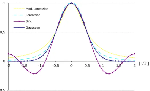
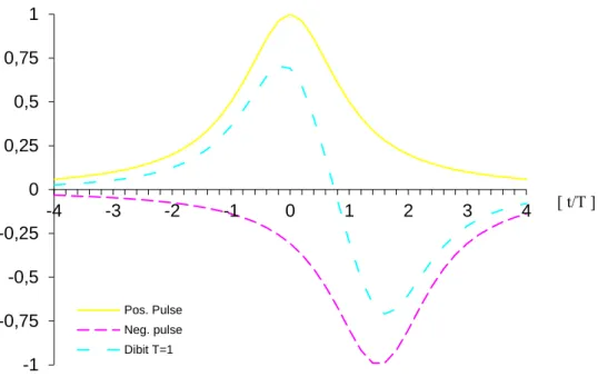
Bit density ...35 Lorentzian model ...37 Alternative models ...39 Dibit response ...40 Offtrack interference ...42 2.7 Disk-drive electronics... 42 Head pre-amplifier ...43 Read/write channel ...44 Host interface ...44 Servo controller ...44
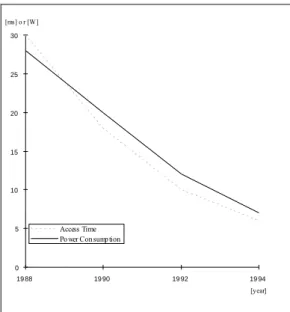
2.8 Market trends and evolution ... 45
2.9 Conclusions ... 48
xix Contents
Chapter 3
Coding techniques and read channel
architectures
51
3.1 Introduction ... 53
3.2 Filtering and equalizing ... 53
3.3 NRZ and NRZI coding ... 56
Non-return to zero inverted on 1s (NRZI)...56
3.4 Run-length limitation ... 57
3.5 Peak detection channel ... 58
3.6 Partial response maximum likelihood channels ... 59
3.7 Decision feedback equalization channel ... 63
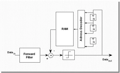
3.8 RAM decision feedback equalization channel ... 64
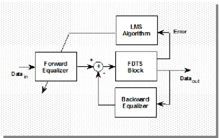
3.9 Fixed-delay tree search with decision feedback channel ... 66
3.10 Multilevel decision feedback equalization channel . 67 References ... 68
Chapter 4
Forward equalizer for MDFE read
channels
101
4.1 Introduction ... 1034.2 Forward equalizer design ... 104
4.3 Read-head pulse shape ... 105
4.4 Channel architecture and equalizer design ... 106
4.5 Adaptive gm-C architectures ... 108
4.6 Canonical structure ... 109
4.7 Orthonormal structure ... 110
Features ...112
4.8 Adaptive capacitor array ... 114
4.9 Transconductors ... 115
Contents xx
Frequency response ...116
Transient response ...118
4.11 Least mean squares algorithm ... 123
4.12 Tuning schemes ... 123
Master-slave filter tuning ...123
References ... 124
Chapter 5
Implementation of transconductor
cells
75
5.1 Introduction ... 775.2 Available transconductors ... 77
5.3 Differential pair transconductor with active load ... 78
5.4 Differential pair with source degeneration transconductor ... 81
5.5 Pseudo-differential transconductor ... 82
5.6 Self-biased balanced pseudo-differential transconductor ... 82
Technology assessment ...83
Balanced transconductor with self-biased feedback .85 Optimum auto-biasing for minimum mismatch effects ...88
Noise ...90
Distortion, PSRR and GSRR ...91
Results and discussion ...93
5.7 Conclusions ... 95
xxi Contents
Chapter 6
Design and evaluation of application
circuits
129
6.1 Introduction ... 131
6.2 An application example to servo demodulation (AT78C1000) ... 132
Off-track interference ...135
Peak detect servo burst demodulator ...137
Area detect servo burst demodulator ...138
Continuous-time integrator ...140
Programmability and gain adjustment ...141
Frequency response ...142
Transient response ...143
6.3 Experimental results of MDFE equalizer (MDFE– 04) ... 145
MDFE–AP02 integrated circuit ...148
MDFE–AP04 integrated circuit ...148
Self-biased trasconductor for VHF applications ...150
6.4 Master-Slave topology filter combined with a bandgap voltage reference ... 159
6.5 Conclusions ... 159
References ... 160
Chapter 7
Conclusions and future work
163
7.1 Conclusions ... 1657.2 Future research suggestions ... 166
Silicon implementation of a fully integrated mixed-signal disk-drive manager CHIP ...167
References ... 168
Contents xxii
Differential pair in bipolar technology ...169 Differential pair in CMOS technology ...173
Annex B: Bandgap voltage reference ... 179
Bandgap voltage reference (BG004) ...179
References ... 184
xxiii Contents
Figure index
Fig. 2.1 – Physical components of a magnetic disk drive storage system. ...17 Fig. 2.2 – Data flux between the disk media and the read and write circuitry. ...19 Fig. 2.3 – Perpendicular to disk magnetic recording. ...24 Fig. 2.4 – Magnetic flux generated by a n-turn. ...27 Fig. 2.5 – Interaction between the magnetic head and the disk surface during the
saturation recording procedure. ...30 Fig. 2.6 – Interaction between the magnetic head and the disk surface during the
saturation recording procedure. ...31 Fig. 2.7 – Write current in saturation recording. ...32 Fig. 2.8 – Stored magnetic flux in saturation recording...33 Fig. 2.9 – Stored magnetic induction in saturation recording. ...33 Fig. 2.10 – Write pre-compensated pulse shape. ...34 Fig. 2.11 – Lorentzian model pulse shape. ...37 Fig. 2.12 – Lorentzian model amplitude spectrum. ...39 Fig. 2.13 – Normalized read head step response models. ...40 Fig. 2.14 – Dibit pulse shape...41 Fig. 2.15 – Dibit pulse shape for different bit densities. ...41 Fig. 2.16 – Disk-drive electronic blocks diagram. ...43 Fig. 2.17 – Storage Capacity and Data Rate evolution for High End drives. ...46 Fig. 2.18 – Consumption and Access Time evolution of High End drives. ...47 Fig. 2.19 – Size evolution. ...48 Fig. 2.20 – Consumption evolution. ...48 Fig. 3.1 – Non-return to zero (NRZ) coding. ...56 Fig. 3.2 – Non-return to zero inverted (NRZI) on ones coding. ...56 Fig. 3.3 – Peak detection block structure. ...59 Fig. 3.4 – Block diagram of a PRML read channel. ...60 Fig. 3.5 – Decision feedback equalization block diagram. ...64 Fig. 3.6 – Block diagram of a RAM-based decision feedback read channel. ...65
Contents xxiv
Fig. 3.7 – Block diagram of a fixed delay tree search with decision feedback read channel. ...66 Fig. 3.8 – Binary tree search structure. ...67 Fig. 3.9 – Block diagram of a multilevel decision feedback equalization read
channel. ...68 Fig. 4.1 – Impulse response versus Lorentzian Model. ...106 Fig. 4.2 – Block diagram of MDFE read-head channel. ...107 Fig. 4.3 – S-plane representation of ideal a priori pole locations. ...108 Fig. 4.4 – Canonical structure. ...109 Fig. 4.5 – Orthonormal structure. ...111 Fig. 4.6 – Integrating capacitors are formed by a fixed capacitor in parallel with a
digitally controlled capacitor-array...114 Fig. 4.7 – Balanced pseudo-differential transconductor. ...116 Fig. 4.8 – Frequency response of the canonical filter structure, for nominal
integrating capacitance values. ...117 Fig. 4.9 – Frequency response of the orthonormal filter structure, for nominal
integrating capacitance values. ...118 Fig. 4.10 – Dibit-response of the 2nd order and 3rd order allpass equalizers. ...119
Fig. 4.11 – Dibit-response of the Allpass Filter. ...120 Fig. 4.12 – Layout of active circuitry...121 Fig. 5.1 – Schematic of a source-coupled differential pair transconductor. ...78 Fig. 5.2 – Current output of a differential-pair transconductor with active load. ..79 Fig. 5.3 – Differential output of a differential-pair transconductor with active
load. ...80 Fig. 5.4 – Schematic of a source-coupled differential pair with source
degeneration transconductor. ...81 Fig. 5.5 – Schematic of pseudo-differential pair transconductor. ...82 Fig. 5.6 – Schematic of gm. ...86 Fig. 5.7 – Self-biased connection in a first order low-pass filter...87 Fig. 5.8 – Ideal common-mode voltage for the gm. ...89
xxv Contents Fig. 5.9 – DC biasing is self-imposed by the feedback loops established in a filter
implementation. ...90 Fig. 5.10 – Common mode rejection ration of the equalizers (>80dB). ...92 Fig. 5.11 – Power source rejection ratio of the equalizers (>45dB). ...92 Fig. 5.12 – Ground source rejection ratio of the equalizers (>45dB). ...93 Fig. 5.13 – Frequency response of the pseudo-differential transconductor. ...94 Fig. 5.14 – Frequency response of gm with 100K output load (Iout+ and Iout-). ....94
Fig. 6.1 – Servo sectors in the hard disk. ...132 Fig. 6.2 – Servo sector information format. ...133 Fig. 6.3 – Servo bursts field format. ...134 Fig. 6.4 – Offtrack interference. ...136 Fig. 6.5 – Peak detect servo burst demodulator architecture. ...137 Fig. 6.6 – Peak detect servo burst demodulation waveforms...137 Fig. 6.7 – Rectified peak detect servo burst demodulation waveforms. ...138 Fig. 6.8 – Area detect servo burst demodulator architecture. ...139 Fig. 6.9 – Area detect servo burst demodulation waveforms...139 Fig. 6.10 – Area integrator implementation. ...140 Fig. 6.11 – Area integrator core schematics...141 Fig. 6.12 – The integrating capacitor consists of a digitally controlled
capacitor-array. ...141 Fig. 6.13 – Frequency response of the area integrator for nominal integrating
capacitance values. ...143 Fig. 6.14 – Transient response of the area integrator to a sequence of Lorentzian
pulses for integrating capacitance values of 10pF, 20pF, 30pF,
40pF. ...144 Fig. 6.15 – PCB layout top view. ...146 Fig. 6.16 – PCB layout bottom view. ...146 Fig. 6.17 – Layout and floor-plan of MDFE-04. ...147 Fig. 6.18 – Top view of MDFE-04. ...149 Fig. 6.19 – Simulated frequency response of the allpass filter (Ireal and Iideal). ...150
Contents xxvi
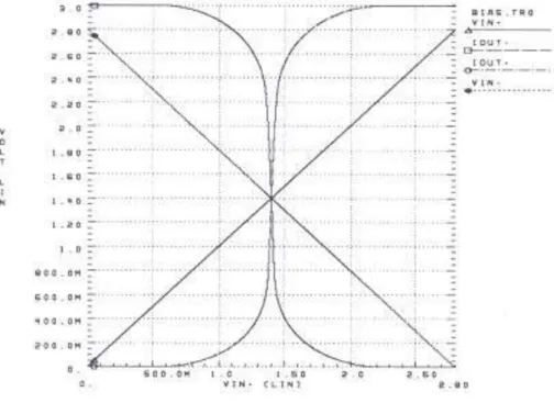
Fig. 6.21 – MDFE-04 test setup. ...151 Fig. 6.22 – Simulation result for the DC characteristic of the transconductor
cell...152 Fig. 6.23 – Measured result of the DC characteristic of the transconductor cell. ..153 Fig. 6.24 – Frequency response of the pseudo-differential transconductor. ...154 Fig. 6.25 – Simulation results for the frequency response of the transconductor cell (Iout+ and Iout-). ...155
Fig. 6.26 – Frequency response of the transconductor cell (Iout+ and Iout-). ...156
Fig. 6.27 – Frequency response of the transconductor cell (Iout+). ...156
Fig. 6.28 – Bonding wire and pico-probe electromagnetic coupling. ...157 Fig. 6.29 – Coupling effect of pico-probe at 80MHz...157 Fig. 6.30 – Harmonic distortion of the transconductor cell. ...158 Fig. 7.1 – Disk-drive electronic blocks diagram. ...167
xxvii Contents
Table index
Table 1.1 – Equalizer evolution. ...7 Table 1.2 – PRML channel evolution. ...8 Table 2.1 – ISI influence on peak value shift and decrease. ...42 Table 2.2 – High End disk evolution. ...46 Table 2.3 – Low End disk drive evolution. ...47 Table 3.1 – RLL (1,7) coding. ...58 Table 3.2 – Partial response variants. ...61 Table 3.3 – PRML channel evolution ...63 Table 4.1 – Main characteristics of the allpass filter. ...122 Table 4.2 – Equalizer evolution. ...123 Table 5.1 – Characteristics of the MOS transconductor. ...95 Table 6.1 – Main characteristics of the area integrator filter. ...145 Table 6.2 – Electrical characteristics of the transconductor cell. ...159
xxix Contents
List of abbreviations and symbols
ADC ... Analog to Digital Converter
ATA ... Advanced Technology Attachment (PATA)
ATAPI ... Advanced Technology Attachment Packet Interface BSIM ... Berkeley Short-channel IGFET Model
CPP ... Current Perpendicular-to-Plane CT ... Continuous-Time
CMOS ... Complementary Metal-Oxide-Semiconductor CMRR ... Common Mode Rejection Ratio
DAC ... Digital to Analog Converter DFE ... Decision Feedback Equalization DMA ... Direct memory access
DSP ... Digital Signal Processor
ESS ... European Silicon Structures (ES2) EOT ... Equivalent Oxide Thickness
EPRML ... Extended Partial Response Maximum Likelihood FDTS ... Fixed Delay Tree Search
ft ... Transition frequency
gm ... Transconductance (or transcondutor)
GMR ... Giant Magnetoresistance GSRR ... Ground Supply Rejection Ratio LMS ... Least Mean Squares
LPF ... Low Pass Filter HDD ... Hard Disk Drive IC ... Integrated Circuit
IDE ... Integrated Drive Electronics (ATA)
MDFE ... Multilevel Decision Feedback Equalization MLSD ... Maximum-Likelihood Sequence Detector
Contents xxx MR ... Magnetoresistance
NMOS ... N-type Metal-Oxide-Semiconductor NCQ ... Native Command Queuing
OTA ... Operational Transconductor Amplifier ISI ... Intersymbol Interference
IGFET ... Insulated-Gate Field Effect Transistor PCB ... Printed Circuit Board
PCMCIA .... Personal Computer Memory Card International Association PLL ... Phase-Locked Loop
PLO ... Phase-Locked Oscillator
PMOS ... P-type Metal-Oxide-Semiconductor PR ... Partial Response
PR4 ... Partial Response (class 4)
PRML ... Partial Response Maximum Likelihood PSRR ... Power Supply Rejection Ratio
PTAT ... Proportional To Absolute Temperature RAID ... Redundant Arrays of Inexpensive Disks RAM-DFE ... RAM-based Decision Feedback Equalization RLL ... Run–Length Limitation
SAR ... Successive Approach Register SATA ... Serial ATA
SCSI ... Small Computer System Interface SNR ... Signal Noise Ratio
SSD ... Solid-State Drive
THD ... Total Harmonic Distortion TMR ... Tunneling Magnetoresistance UDMA ... Ultra DMA
UMTS ... Universal Mobile Telecommunication System VGA ... Variable Gain Amplifier
1
Chapter 1
Introduction
Objectives 3 Motivation 3 Context and state of the art 5 Layout of the thesis 8 Original contributions 93 Introduction
1.1
Objectives
The goal of this work is to conceive, design and test a low voltage, low power adap-tive continuous time 3rd order allpass equalizer implemented in a 0.5m standard digital
CMOS process, for use in a magnetic disk DFE read channel. The filter has been inte-grated using a gm-C topology for better high frequency performance. An orthonormal-based structure adopted for the sake of adaptability is presented, along with a low-mis-match high bandwidth transconductor. The gms are pseudo-differential balanced trans-conductors and the integrating capacitors are implemented using polarized transistor ar-rays consisting of 12.5fF unit size cells. The parasitic input capacitance in the gms is subtracted from the respective integrating capacitors thus allowing the transconductors to work at very high frequency. Automatically tuning the frequency of poles compensates for process tolerances that influence the effective value of the active devices. The pro-posed system is particularly efficient in the fast growing market of portable computer applications.
1.2
Motivation
The motivation of this work was the search for continuous time filtering solutions for reading in data recording and reproduction systems on magnetic media, with costs and consumption (total size less than 1mm2 and consumption than 1mW/pole), lower than the
circuits available. Accordingly, as was done in this work, the rapid development of mi-croelectronics technology raised very significant efforts worldwide in order to investigate new techniques for implementing such filters in monolithic integrated circuit, especially in CMOS technology (Complementary Metal Oxide Semiconductor). We present a com-parative study on different hierarchical levels of the project, which led to the realization and characterization of solutions with the desired characteristics.
In the first level, this study addresses the question of recording and transmission of signal and the choice of good mathematical models for the processing of information and
Introduction 4
minimization of error, inherent to the approaches in accordance with the physical princi-ples of the characterized devices.
The work's main thesis is focused on the hierarchical levels of the architecture of the read channel and integrated circuit implementation of its main block - the block of filtering. At the architecture level of the read channel, it presents a comprehensive study on existing methodologies and adaptation of signal recovery of data on magnetic media. This project appears in the proposed solution for a low-cost, low consumption, low volt-age, low complexity, based on CMOS digital technology, to implement a DFE (Decision Feedback Equalization) based equalizer of the signal using continuous time integrated analog filters.
At project level of implementation of the filtering block and techniques for imple-menting its constituents, it was concluded that the technique based on transconductance (gm) and capacitors, also known as gm-C filters is the most appropriate for achieving adaptive filter in very-high-frequency. In this lower level, two sub-levels of depth of study in this thesis are defined, namely: research and analysis of structures for optimal design of filters using state-space representation, and the study of techniques for implementation in digital CMOS circuits for transconductance for the implementation of integrated ana-log filters in continuous time. Following this study, we compare two structures of filters in the space of states, corresponding to two alternatives for achieving an adaptive equal-izer by a continuous-time third order allpass filter, for use in a channel of reading data on magnetic media.
As a constituent part of these filters, we present a technique for the realization of a transconductance cell and integrating capacitors using linear arrays of MOSFET transis-tors for signal processing in very-high-frequency integrated circuit using sub micrometric CMOS technology. There are methods capable of automatic adjustment to compensate for the errors against the nominal values of components due to the manufacturing toler-ances for which we present the simulation results and experimental measurements ob-tained.
Also as a result of this study, we designed an adaptive first order filter based on the proposed transconductance cell and using the same equalization techniques. This block
5 Introduction is proposed to control positioning of the head of reading systems in recording/playback data on magnetic media.
1.3
Context and state of the art
The first solutions in magnetic hard disk drives for personal computers were pro-posed in 1980 closely followed by the first 3 1/2" floppy drives in 1981. Early designs used conventional peak-detection read channels, basically relying on zero crossing of the differential input signal, to sample the input in its local minimum or maximum value. These designs have gradually evolved to present days including equalizer blocks for pulse-slimming and more complex clock recovery schemes.
The main limitation of peak detection read channels is that the data-encoding scheme doesn’t allow the use of more aggressive data storage techniques based on the augment of user bit density. This limitation in linear data density strongly compromises the desired storage capacities, whilst maintaining slow data transfer speeds based on sin-gle peak detection schemes. As bit density is increased, these analog peaks are processed at higher rates, thus significant overlapping occurs, leading to inter-symbol interference (ISI) and possibly to data bit errors.
In 1990 IBM introduced its first-generation partial-response1 maximum likelihood
(PRML) read channel technology in hard disk-drives [1.1]. The PRML approach differs from traditional peak detector read channels, which do not compensate for ISI, by using advanced digital filtering processing to shape the read signal frequency and timing char-acteristics to a desired partial response, and by using maximum-likelihood digital data detection to determine the most likely sequence of data bits that was written to the disk. This sequence-detection method is implemented using the Viterbi2 algorithm for
se-quence detection [1.2].
1 Partial Response (PR) coding in magnetic recording was first proposed by Hisashi Kobayashi in 1970. 2 Andrew Viterbi invented this algorithm in 1967 for decoding convolutionally encoded data.
Introduction 6
PRML based read channels use an analog to digital converter to sample the input read head signal and advanced digital signal processing (DSP) to allow higher bit density at faster data rates with improved data integrity. The increase in the amount of allowed ISI is compensated at the cost of complexity, power and silicon area. This is particularly significant and relevant considering the desirable increase in data speed, especially due to the power consumption increase with the operation frequency.
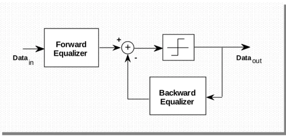
Alternative architecture delivering equivalent performance to the most advanced partial response read channel solutions, were presented [1.3] based on decision feedback equalization (DFE)3. The basic DFE architecture consists of two equalizing finite impulse
response (FIR) filters and a slicer. The forward equalizer is used for precursor ISI can-cellation and the backward equalizer is a non-linear post cursor ISI remover.
This is the common structure from which derived some of the schemes described in chapter 3, such as fixed-delay tree search decision feedback (FDTS/DF), RAM-based DFE (RAM-DFE)4 and multilevel decision feedback equalization5 [1.5] (MDFE).
In August 1996, Philips Semiconductors announced its first standard RAM-DFE read channel device [1.6], a fully-adapted self-training DFE scheme compatible with a wide range of read head and media interfaces. Adaptation allows improved bit-error rate (BER) achieving signal-to-noise ratio equivalent to PR4 read channel, at increased user data bit density.
Considerable effort was employed in the developing of a low power continuous time adaptive forward equalizer alternative to the FIR approach usually used with DFE.
3 Decision Feedback Equalization (DFE) was first presented in 1967, by M. Austin as an equalizing
tech-nique for dispersive channels. Adaption capability was further proposed and added to the system in 1970 by D. George et al., but it was only in 1996 that this scheme was firstly integrated in a commercial circuit as a practical alternative to peak detection techniques
4 The first DFE equalizer using RAM-Based equalization [1.4] was published in 1989 by Fisher et al. 5 Multilevel Decision Feedback Equalization (MDFE) was first presented in 1993, by J. Kenney as an
7 Introduction In February 1995, Professors José Epifânio da Franca and John Kenney proposed the development of a continuous-time filter solution for the realization of the forward equalizer as the starting problem to be addressed by the work developed in this thesis. This work was carried out at the integrated circuits and systems group in IST until 2000 and later on completed and written under the supervision of professors Augusto Albu-querque and Francisco Cercas at ISCTE.
The following tables summarize the most relevant publications in the implementa-tion of PRML read channels and the main characteristics in terms of technology, data rate, power and area of the equalizer solutions presented. Table 1.1 shows the character-istics of available equalizers and Table 1.2 the total area and power consumption of PRML solutions.
Table 1.1 – Equalizer evolution.
Year Technology Freq./Data rate Power Area
1993 1.0m CMOS 7.1 MHz 988 mW 146 mm2 1993 2.0m CMOS 40 MHz 500 mW 31 mm2 1994 1.2m CMOS 100 MHz 900 mW 44 mm2 1995 0.8m CMOS 240 MHz 426 mW 2.9 mm2 1995 0.5m BiCMOS 250 MHz 340 mW 1.8 mm2 1996 0.6m CMOS 200 MHz 507 mW 13 mm2 1996 1.0m CMOS 160 MHz 460 mW 23 mm2 1997 0.6m CMOS 150 Mb/s 90 mW 0.8 mm2 1998 0.25m CMOS 360 Mb/s 21 mW - 1999 1.0m CMOS 80 Mb/s 280 mW 6.7 mm2 2002 0.5m CMOS 100 Mb/s 130 mW 1.3 mm2 2005 0.18m CMOS 70 MHz 21.8 mW - 2007 0.18m CMOS 160 MHz 15 mW - 2008 0.18m CMOS 400 MHz 80 mW -
Introduction 8
Table 1.2 – PRML channel evolution.
Year Technology. Data Rate Power Area 1994 0.8m BiCMOS 64 Mb/s 2.85 W - 1994 1.0m BiCMOS 72 Mb/s 0.78 W - 1994 0.8m CMOS 36 MHz 0.69 W 51 mm2 1995 0.5m BiCMOS 16 MB/s 1.20 W 26 mm2 1996 0.6m CMOS 130 Mb/s 1.35 W 28 mm2 1996 0.7m BiCMOS 150 Mb/s 1.55 W 47 mm2 1996 0.5m BiCMOS 200 Mb/s 0.85 W 20 mm2 1999 0.35m CMOS 300 MHz 0.23 W 0.8 mm2 2001 0.18m CMOS 150 Mb/s 0.18 W 1 mm2 2006 0.35m CMOS 300 MHz - 12.8 mm2
1.4
Layout of the thesis
The first chapter of the thesis introduces the subject of study, its overall motivation and the objectives pursued during this work. It also describes the structure of the docu-ment and statedocu-ment of originality of the proposed solutions.
The second chapter of this thesis is a brief characterization of the physical elements involved in the magnetic disk storage process. The basic theoretical definitions and mod-els of the read channel are introduced. The read and write processes in magnetic storage are explained together with the definition of simple key concepts such as user bit density and intersymbol interference. The building blocks of disk drive electronics are identified and succinctly described. A general analysis of magnetic disk drive products available on the market is summarized in terms of expectable evolution in main characteristics of the device.
9 Introduction The third chapter introduces the existing coding algorithms involved in the storage and readback process of magnetically stored information and the basic read channel ar-chitectures. Run length limitation and its advantages in band limited communication channels is explained. The principal read channel architectures are described and com-pared in terms of performance. Partial Response and Multilevel Decision Feedback Equalization (MDFE) read channel architectures are introduced.
The forth chapter presents two practical solutions for the forward equalizer in MDFEs architecture, the critical block of the system. Recursive continuous-time adaptive filters are proposed for the implementation of equalizers for magnetic disk drive read channels. A canonical structure and an orthonormal structure recursive filter are proposed and compared at transistor level. Tuning schemes and LMS algorithms are analyzed.
The fifth chapter introduces the building blocks of the proposed circuits. A self-biased transconductance cell is presented for the implementation of very high frequency current mode gm-C filters. The influence of short channel effects is analyzed. The use of biased MOSFET capacitor arrays in standard digital CMOS technology is studied.
Chapter six describes the experimental procedure and results of the proposed inte-grated circuits. Firstly it presents a continuous time servo burst demodulator for magnetic disk drives based on the building blocks introduced in chapter five. Secondly it presents simulation and measurement results of the continuous time equalizers and of the trans-conductor cell proposed.
The seventh and final chapter summarizes the conclusions of this thesis and pre-sents some suggestions for further research and development.
1.5
Original contributions
The original contributions of this thesis are:
Development of a fully analog continuous-time integrated equalizer for the implementation of a multi-level decision feedback equalization (MDFE) read channel [1.7] (Chapter 5 ).
Introduction 10
Proposal and development of an orthonormal state-space current-mode fil-ter for the implementation of a continuous-time third order adaptive equal-izer for MDFE [1.7] (Chapter 5 ).
Comparison of orthonormal and canonical filter structures based on the physical limitations at circuit-level design with simulated and measured re-sults [1.7] (Chapter 5 ).
Development of an auto-biased 0.5m CMOS transconductor cell for the implementation of very high frequency current-mode gm-C filters [1.8] (Chapter 4 ).
Proposal and development of a first order filter for servo-burst demodula-tion in magnetic read channels [1.9] (Chapter 6 ).
Comparison of different design approaches to equalization in hard disk read channels [1.10].
References
[1.1] H. Kobayashi and D. Tang, “Application of Partial-Response Channel Coding to Mag-netic Recording Systems”, IBM Journal of Research and Development, pp. 368-375, Jul. 1970.
[1.2] A. J. Viterby, “Error bounds for convolutional codes and asymptotically optimum decod-ing algoritm”, IEEE Trans. Information Theory, vol. IT-13, pp. 260-269, 1967.
[1.3] M. E. Austin, “Decision-Feedback Equalization for Digital Communication Over Disper-sive Channels”, MIT/RLE, Tech. Rep. 461, Aug. 11, 1967.
[1.4] K. Fisher, J. Cioffi and C. M. Melas, “An Adaptive DFE for Storage Channels Suffering from Non-linear ISI and Transition Dependent Noise”, ICC 89, Boston, Jun. 1989. [1.5] John G. Kenney, L. Richard Carley and Roger W. Wood, “Multi-level Decision Feedback
Equalization for Saturation Recording”, IEEE Trans. on Magn., vol. 29, no. 3, pp. 2160-2171, Jul. 1993.
[1.6] Nicholas P. Sands et al., “A 200Mb/s Analog DFE Read Channel”, ISSCC Digest of Tech.
11 Introduction [1.7] Nuno Garrido, J. Franca, and J. Kenney, “A Comparative Study of Two Adaptive
Con-tinuous-Time Filters for Decision Feedback Equalization Read Channels”, Proc. IEEE Int. Symp. on Circuits and Systems (ISCAS), vol. 1, pp. 89-92, Jun. 1997.
[1.8] Nuno de F. Garrido and José E. Franca, “An Auto-Biased 0.5m CMOS Transconductor for Very High Frequency Applications”, Proc. IEEE Int. Symp. on Circuits and Systems (ISCAS), vol. 1, pp. 325-328, Jun. 1998.
[1.9] Nuno de F. Garrido and José E. Franca, “A Continuous-Time Area Detector Servo De-modulator for Hard Disk Drives”, Proc. IEEE Int. Conf. on Electronics, Circuits, and Systems (ICECS), vol. 2, pp. 127-130, Sept. 1998.
[1.10] Nuno de F. Garrido and Francisco A. B. Cercas, “Equalization in Hard Disk Drive Read Channels”, Proc. IEEE Int. Conf. on Telecommunications (ICT), pp. 390-394, May 2014. [1.11] Nuno de F. Garrido, “BG004 Bandgap Voltage Reference”, Tech. Report, ATMEL/ES2,
Fab7, Rousset (France), Mar. 1997.
[1.12] Nuno de F. Garrido, “Design of Analog Cells for AT78C1000”, Tech. Report, ATMEL/ES2, Fab5, Colorado Springs (USA), Apr. 1997.
[1.13] Nuno de F. Garrido, “Experimental Evaluation of VHF Equalizers for Decision Feedback Equalization Magnetic Read Channels”, Tech. Report, Fab5, Colorado Springs (USA), Aug. 1997.
13
Chapter 2
The recording and readback
processes
Nonvolatile memory storage devices 15 Physical aspects of the hard disk 16 Playback process 19 Write process 24 Read back channel model 35 Disk-drive electronics 42 Market trends and evolution 45 Conclusions 48
The recording and readback 14 process
15 The recording and readback process
2.1
Introduction
This chapter describes the physical elements and principals involved in the mag-netic disk storage process. The basic theoretical definitions and models of the read chan-nel are introduced. The read and write processes are explained together with the definition of simple concepts such as user bit density and intersymbolic interference. The building blocks of disk drive electronics are identified and succinctly specified. A general analysis of magnetic disk drive products available on the market is summarized in terms of ex-pectable evolution in the main characteristics of the device.
2.2
Nonvolatile memory storage devices
Nonvolatile memory devices are crucial to complex systems allowing information to be safely and persistently stored in the absence of power consumption. This is relevant either for massive storage systems as well as for mid-sized systems requiring little more than start-up code storage.
The first solutions for nonvolatile memory come from the fifties with magnetic tape drives in mainframe computers. Slow head positioning and sequential access where strong limitations for this early devices. Magnetic hard drives and floppy drives where proposed in 1981 providing fast head positioning on disk and hence low access time to stored data. In a hard disk drive (HDD) the non-volatile storage is accomplished through digitally storing the data on rapidly spinning platters with a magnetic surface platter. This is a circular disc which has a magnetic surface that stores the data. The first HDDs had multiple platters usually made of aluminum with a thin film carbon coating applied to each side.
E2PROM and Flashrom, where originally used to keep a copy of firmware images such as BIOS. More recently, in 2011, solid-state drive (SSD) have reached the market of nonvolatile data storage for personal computers. These devices use integrated circuit memory to store data persistently and electronic interfaces compatible with traditional block input/output interface of traditional hard disk drives. Since SSDs have no moving mechanical components, the access time is extremely low, and power consumption is also low when compared to HDD. The stored bits are safer in a SSD and the device is more
The recording and readback 16 process
robust than a conventional HDD. For these reasons, some predict that in time SSD may overtake HDD as the preferred nonvolatile media. Nevertheless, the low price per TB for the HDD devices, is much lower than that of SSD devices, making HDD a growing mar-ket for years to come.
2.3
Physical aspects of the hard disk
Magnetic support has long been the prime choice for non-volatile data storage. More particularly, magnetic disk drives have taken an increasingly greater share of these tasks. The physical characteristics of magnetic disk devices are a fine match for the re-quirements of swift and non-sequential recording and playback of digitally stored data. Unlike their magnetic storage predecessors, magnetic disk drives have rapidly evolved to combine: mass storage capability, fast sequential access and long-term reliability akin to magnetic tape devices; with the inexpensive, flexible and efficient non-sequential access of floppy-disk drives. Moreover, the widespread use of this device has rapidly pushed its performance way beyond these magnetic storage counterparts in all relevant parameters. These wide range high performance uniqueness meet in a fine compromise, that allow its use as a virtual random access memory expander as efficient as its use in the hosting of massive long-standing secure data banks.
Although some still proudly preserve some amazing prototypes of huge size alumi-num disks used during the early ages of magnetic disk storage, mass production of desk-top computer magnetic disks quickly matured to fit in 3 ½” bays. With the advent of portable computers, regular pushes towards slender and lighter laptop equipment have further forced magnetic disk devices from 3.5” to 2.5”, 1.8” or even 1.3”. Recent market available applications present a complete 0.85” disk-drive solution of traditional archi-tecture scaled to fit a thumbnail, defying the obvious appeal of massive non-volatile Flash memories.
Regardless of its size, the basic physical components of a magnetic disk storage apparatus are depicted in Fig. 2.1.
17 The recording and readback process Fig. 2.1 – Physical components of a
magnetic disk drive storage system.
A magnetic disk device mainly consists of four basic physical components:
· One or several aluminum disks, each providing an endurable physical foothold for the thin magnetic film coating that contains all the information stored on the disk. · The head actuator or servo actuator that is responsible for the positioning6 of the
magnetic head in a random track on the disk.
· The read head7 at the end of the actuator arm floats merely nanometers8 over the magnetic film coating, and caries out the sensing and imposing of the magnetic fields from and onto the media as the disk data is read or written.
· The spindle motor is used to steer the movement of the disk(s), spinning its angular velocity up to 10000 revolutions per minute (rpm). This motor is accountable for about 40% of the total disk drive power.
6 This time is usually defined as access time, and is one of the main characteristics of the disk along with
total capacity and data transfer rate.
7 Usually made of high permeability alloy to improve flux sensibility.
8 The mechanical principals and physical dimensions are akin to other magnetic storage systems such as
digital videotape recorder or VHS.
Alu minu m Dis k
Ac t ua ct or In du ct ive Hea d
The recording and readback 18 process
The magnetic film surface veneers, with approximately two thousand circular con-centric tracks9 per centimeter, contain all the information on tiny independently oriented
magnets. These slight magnetic records are packed at approximately 40000 bits per cen-timeter yielding out binary encoded data.
The magnetic tracks on the media surface are narrow concentric rows of very small magnets containing user information. These magnets can have one of two possible orien-tations: clockwise (left) or anti-clockwise (right) — see Fig. 2.2 — such that a transition from left to right (or right to left) in the magnetic orientation induces a voltage across the coil proportional to the flux variation with time, as given by Faraday’s law of induction, represented in equation (2.4).
The user bit10 is recorded on the disk surface driven by a magnetic flux throughput
imposed on the magnetic head during the write process. Once stored, the bit can be sensed during playback as a very low amplitude11 voltage pulse that is subsequently processed
and transmitted by the read circuitry back to the data bus via the host interface controller. Fig. 2.2 shows the data flux between the disk media and the read/write circuitry. The electronic front-end is usually a dedicated pre-amplifier integrated circuit physically placed close to the head, with large bandwidth and low noise specifications used for gain boosting of these low voltage pulses. This IC separates the signal path into two split dif-ferential data channels, one for writing and one for reading. Both continuous time differ-ential signals are analog interfaces between the read/write channels and the front-end electronic blocks involved in the magnetic storage and read back processes.
9 The tracks are further divided in angle defined portions (like pie cuts) called sectors, each having 512
bytes of user data preceded by a header containing servo fields for correct track positioning and monitoring, and by preambles that assist in gain setting and clock recovery.
10 Logical 1 if there is a transition on flux magnetization (either left to right or right to left) and logical 0 if
no transition occurs.
19 The recording and readback process Fig. 2.2 – Data flux between the disk media
and the read and write circuitry.
2.4
Playback process
The playback process starts when the host interface controller receives a read order from the host processor. The command is usually originally initiated by the CPU and is issued onto the disk electronic blocks through a SCSI12 or IDE13 bus controller IC. The
host interface controller forwards the order to the servo controller, which in turn positions the head actuator onto the designated track, according to the track ID stored on the servo sectors. Once the head is in a fixed position, the rotating movement of the disk allows that the read channel IC can correctly access and feedback the stored user data to the host interface controller. The worst-case elapsed time between data request and data ready at the bus is defined as the access time of the disk. Due to the involved complexity and
12 Small Computer System Interface is a high-speed parallel interface standard defined by the American
National Standards Institute (ANSI) used for connecting microcomputers to peripheral devices.
13 Integrated Device Electronics is one of the most widespread disk-drive interface, in which the controller
electronics reside on the drive itself, eliminating the need for a separate adapter card and offering ad-vantages such as look-ahead caching.
+ -+ -Pre-Am plifier Head Spindle Disk Media to Read Channel n-Turn Coil + -+ -from Write Channel
The recording and readback 20 process
physical constraints this access time is usually in the order of 10 to 20 milliseconds. Nat-urally this significant delay overhead is negligible in the general case of sequential disk access to large data blocks. Moreover, in most cases, the host interface controller buffers the read data in local memory blocks14, before being transferred back to the host
proces-sor. This is usually combined with sophisticated software disk caching schemes.
Therefore, the fundamental electrical characteristic of the disk is the user data trans-fer rate. Unfortunately, high transtrans-fer rates imply costly consumption requirements15, and
hence, especially in the case of portable systems, the power consumption takes the major role in the achievable balance between speed and battery operation autonomy.
Inductive head
The inductive head hovers over the surface of the disk, at the end of the actuator arm. The traditional inductive head is a C-shaped highly permeable microscopic mag-neto-sensitive alloy embraced by a coiled wire similar to those of ferrite read heads in tape recorders. A wired coil can be used for both reading and writing of bits to the disk surface. By imposing a strong magnetic field in the gap of the C, and thus on the recording surface adjacent to the gap the media can be magnetized. To read a magnetized stored bit, the head generates a current in the coil, when the media rotates past the head core it gen-erating a voltage drop on the wire. In HDD the field is very strong and the gap is quite narrow, determining the minimum size of a recorded bit, and hence, the linear and areal density.
The relative movement of the stored magnets on the disk’s surface in respect to the read head causes a variation of the magnetic flux that flows through the head core. The variation in time of the magnetic flux density flow through an electric circuit wire loop generates an electric field, as results from Faraday’s law expressed in its integral form by
14 See the electric block diagram in Fig. 2.16 on page 42.
15 Note that the power consumption in digital blocks is roughly proportional to the signal frequency, and
21 The recording and readback process
S C ds N B t l d E (2.1)where S represents any surface delimited by the oriented closed path wire contour here denoted as C. VectorB denotes the magnetic flux density and N is a unitary vector
perpendicular to surface S.
The read circuit depicted in Fig. 2.2 can be treated as a simple wire loop with a resistive load, immersed in a time varying magnetic field16, and therefore the potential
difference at the edges of the load is given by the following line integral
t E dl V C
. (2.2)Using the definition of magnetic flux
S dS N B (2.3)and combining it with equations (2.1) and (2.2) indicates that the variation of the magnetic flux, flowing through an electric circuit generates a voltage at the wire termi-nals. This is one of the basic principles of electromagnetic induction as was first stated by Faraday in 1831, and can be expressed in a simplified form by equation (2.4) known as Faraday’s law of induction
dt d t
V( ) . (2.4)
The polarity of the induced voltage and the direction of the electric field through the wire, produce a current flow on the circuit that opposes the change of magnetic flux, as follows from Lenz’s law. The minus signal on equations (2.1) and (2.4) denotes this statement.
The recording and readback 22 process
This also derives from Maxwell’s treatise on electricity and magnetism published in 1873 — closely based on Faraday’s work — on equation (2.5) that expresses the law of induction in its differential form
t B E . (2.5)
This is comprehensible from the application of Stoke’s theorem to the line integral of the electric field E as depicted in (2.6), which yields equation (2.1).
S S C ds N dt B d ds N E l d E (2.6)Therefore, the inductive head effectively implements a magnetic flux intermediate to access the user data stored on the disk surface. Multiple coils of the circuit wire are usually used to embrace the inductive head, hence the effective surface of the n-turn de-limited solenoidal path is equivalent to n times the surface of a single wire loop. This increases the signal strength during the read process, whilst reducing the current neces-sary to generate the desired combined conducted magnetic field during the write process.
As a result equation (2.4) is in this case expressed by equation (2.7)
dt d n t
V() . (2.7)
Consequently, any transition in the magnetic field flowing through the head induces a voltage across the wire proportional to flux variation with time and to the number of coiled turns.
The read and write principals of the inductive head did not change with Metal-in-gap (MIG) or thin-film heads (TFH). In MIG read heads the properties of soft alloys like permalloy (NiFe) improve magnetization saturation, allowing twice the magnetic field. TFH are made using photolithography similar to semiconductor technology, allowing even higher read and write accuracy.
23 The recording and readback process Magnetoresistance (MR) and giant magnetoresistance (GMR)
An improvement was to create a separate head using the magnetoresistive (MR) effect which changes the resistance of a material in the presence of magnetic field. MR heads are able to read very small magnetic features reliably, but cannot be used to create the strong field used for writing. The term AMR (A=anisotropic) is used to distinguish it from the later introduced improvement in MR technology called GMR (giant magnetore-sistance). The introduction of the AMR head in 1996 by IBM led to a period of rapid areal density increases of about 100% per year. In 2000 GMR, giant magnetoresistive, heads started to replace AMR read heads.
Tunneling magnetoresistive (TMR)
In 2005, Seagate introduced the first drives to use tunneling MR (TMR) that can be activated before starting the write operation, hence ensuring that the head's write field fully saturates the magnetic disk medium. This improves the written magnetic transitions and decreases the separation to the disk medium for improved signal strength.
Perpendicular magnetic recording (PMR)
An important advance was the transition to perpendicular magnetic recording (PMR). The main difference being that the write flux is driven perpendicularly to the media as opposed to in parallel to the media. This has implications on the write head format and on the disk media since it implies the use of an additional soft magnetic under layer, serving to augment field strength written to the disk media as shown in Fig. 2.3. The packing of the flux transaction has improved areal density and speed potential.
The recording and readback 24 process
Fig. 2.3 – Perpendicular to disk magnetic recording.
2.5
Write process
The write process is also triggered when the host interface controller receives an order from the host processor, commanding that a given data sequence is stored onto the disk. Typically, some or all of the data will be transferred in advance, packed into blocks and buffered locally. As described for the read process, the servo controller has to position the head actuator onto a designated track. Once the head is in position, the write bits are forwarded to the write channel and are output to the magnetic head, through which they are forced onto the rotating disk. The physical constrains determining the access time during a write procedure are similar to the referred for the playback process. Although the host interface bus and magnetic head are shared for both write and read commands, the write channel and magnetic recording fundamentals justify additional analysis.
Inductive head
The basic principal behind non-volatile recording of a bit on the surface of a mag-netic disk is the establishment of a magmag-netic field imposed by an electric current flow
Underlayer Data Layer Data Layer Longitudinal recording Perpendicular recording Under Layer
25 The recording and readback process through an electric wire. The fundamental law relating magnetic field strength and elec-tric currents was ascertained in 1820 by Biot and Savart, and is expressed in its differen-tial form by equation (2.8), the well-known Biot-Savart law
2 4 r u l d I H d r (2.8)
where dH denotes the differential magnetic field strength, for a given position of
which r and ur are the distance and unit vector respectively. Distance r and vector ur
are referred to an infinitesimal current element denoted as Idl
.
Therefore, the magnetic field strength vector H induced on any position in a
tri-di-mensional space by an electric circuit can be obtained by integrating the influence of all current elements in respect to that point. Hence, this yields equation (2.9), where C de-notes the closed circuit path and is valid for any chosen physical geometry.
C r r u l d I H 2 4 1 . (2.9)A simple inference is that a stationary current, i.e. a constant velocity charge flow, through an electric wire generates a static magnetic field. This basic concept plays an important role in saturation recording17.
The magnetic field denoted by H is non-conservative, this is patent in Ampere’s
law, given by l d H I C
(2.10)where C is a closed oriented path and I is the enclosed current.
The differential form of this law combined with the displacement current density
dt D
d term — introduced by Maxwell’s work — added to the current density vector J