September 2017
José Miguel Vaz da Cunha
[Nome completo do autor][Nome completo do autor]
[Nome completo do autor]
[Nome completo do autor]
[Nome completo do autor]
[Nome completo do autor]
[Nome completo do autor]
Bachelor in Micro and Nanotechnologies Engineering
[Habilitações Académicas] [Habilitações Académicas] [Habilitações Académicas] [Habilitações Académicas] [Habilitações Académicas] [Habilitações Académicas]
Insulator materials for electrical passivation of thin
film solar cells
[Título da Tese]
Dissertation for obtaining the degree of Master of Science in Micro and Nanotechnologies Engineering
Dissertação para obtenção do Grau de Mestre em [Engenharia Informática]
Supervisor: Doctor Pedro Salomé, Group Leader, International Iberian Nanotechnology Laboratory
Co-supervisor: Doctor Hugo Águas, Auxiliary Professor, Faculty of Sciences and Technology, New University of Lisbon
Examination Committee:
Chairperson: Doctor Luís Pereira Rapporteurs: Doctor Joana Pinto
Insulator materials for electrical passivation of thin film solar cells
Copyright © José Miguel Vaz da Cunha, Faculdade de Ciências e Tecnologia, Universidade Nova de Lisboa.
A Faculdade de Ciências e Tecnologia e a Universidade Nova de Lisboa têm o direito, perpétuo e sem limites geográficos, de arquivar e publicar esta dissertação através de exemplares impressos reproduzi-dos em papel ou de forma digital, ou por qualquer outro meio conhecido ou que venha a ser inventado, e de a divulgar através de repositórios científicos e de admitir a sua cópia e distribuição com objetivos educacionais ou de investigação, não comerciais, desde que seja dado crédito ao autor e editor.
v
“The role of the infinitely small is infinitely large.”
vii
Acknowledgements
I would like to start by acknowledging Prof. Doctor Hugo Águas, my Co-supervisor at FCT for accepting my master thesis request and for all the support during these months. I also want to acknowledge my Supervisor Prof. Doctor Pedro Salomé for everything. There are no enough words to thank everything that you did for me. Since the internship, you taught me things that I never imagined. Not only in the professional way, but also in the personal one. More than a supervisor, you were a really good friend. I will never forget the discussions from I learnt so much. I also want to thank all the mem-bers of the INL’s NOA group, namely Sourav Bose and Prof. Doctor Paulo Fernandes. Prof. Doctor Paulo with you I learnt considerably about electrical measurements. Without our discussions and your recommendations, I could not achieve the results that I have. With all the meetings, I learnt a great deal about other topics not directly related with my theme. I want to thank everyone in INL that helped me, without them this stage would not be possible, namely Doctor Yury Kolen'ko and Doctor João Gaspar for letting me use their equipment, Doctor Jérôme Borme for having the patience to answer all my questions and Eng. Helder Fonseca for the grateful help in the clean room during the insulator deposi-tions.
A special acknowledgment to Prof. Doctor Rodrigo Martins and Prof. Doctor Elvira Fortunato due to the creation of this course, Micro and Nanotechnologies Engineering, the first one in Portugal. Moreover, by allowing me, during the course, to use the CENIMAT|i3N and CEMOP facilities that they created, making a huge difference between having just theory lessons, and having the theory lessons jointly with practical ones, in those facilities. Every time that I needed something you were here to help. I also want to thank all the professors in the department that always tried to help us not only in the classes but also outside them, namely Prof. Doctor Luís Pereira, Prof. Doctor Rui Igreja, Prof. Doctor Pedro Barquinha, among many others. I want also to thank Prof. Doctor Manuel Mendes and Eng. Tiago Mateus for the aluminium deposition.
I want to thank Prof. Doctor Joaquim and Eng. Jennifer from University of Aveiro/i3N for the measurements and the PL learning. I really am grateful for the discussions about a completely new theme for me that was not easy to learn. I also want to thank Prof. Doctor Bart Vermang and Eng. Siddhartha Garud for the TRPL measurements at IMEC; and Doctor Adam Hultqvist from Uppsala University for the ALD deposition.
Gostava de agradecer a todos os meus colegas do meu curso e da faculdade que me apoiaram ao longo desta longa jornada de cinco anos. A entreajuda foi enorme e sem dúvida que todos contribuí-ram para a minha aprendizagem. Gostava de agradecer especialmente à Cátia e ao Vasco por todos os bons momentos que passamos, mas também por todas as discussões produtivas. Aprendi imenso com vocês, não só profissionalmente, mas também pessoalmente.
À direção da iNOVAfuture 2016, Cátia, Vasco, Tiago e Pedro foi um ano cheio de descobertas para nós, foi difícil, mas fizemos um excelente trabalho que não teria sido possível sem a vossa motiva-ção e dedicamotiva-ção que tiveram pela causa! Acho que todos crescemos imenso com esta experiência, falo por mim, pois nunca tinha tido tal responsabilidade.
Kateryna Zrazhevska, espero que a nossa amizade dure para a eternidade, ensinaste-me muito, quando tiveste de me dar na cabeça também o soubeste fazer, e sei que sem ti, a faculdade não teria sido a mesma coisa. Admiro-te imenso, admiro a forma como pensas, e abriste-me os olhos para coisas que nunca teria pensado por mim só. Obrigado por tudo!
Durante estes cinco anos estive na melhor residência do país, com as melhores pessoas de sem-pre. Quem lá passou, sabe que somos uma segunda família, vivendo 24 horas por dia, 7 dias por semana juntos. Não podia deixar de agradecer ao Ricardo Silva por me aturar estes cinco anos! Foi em dúvida uma sorte tremenda ter-te como colega de quarto, sempre serás um grande amigo! Ao restante pessoal: Everton, Baixinho, Nuno Batista, Cláudia, Sabrina, Romero, Catarina Nunes, Bárbara Costa, Raposo, Douglas, Élvio, Dinis, Rafael, Vânia Silva, Inês Rosete muito obrigado, nem sempre foi fácil, mas viver em conjunto tem destas coisas, e foi uma experiencia incrível ter-vos como amigos, sempre me recor-darei dos bons momentos que passamos juntos e espero que as aventuras não fiquem por aqui!
Insulator materials for electrical passivation of thin film solar cells
viii
Avelino Morganti Neto, não podia esquecer-me de ti, foste mais um grande amigo que fiz na residência, admiro imenso a tua inteligência e criatividade, mas ainda mais a vontade que tens de mudar o mundo, espero que nunca deixes de ser assim porque vais atingir os teus objetivos de certeza! Sabes que um dia irei ao Brasil visitar-te!
Ao meu padrinho Zé Rui e madrinha Sofia Martins por todo o apoio que me deram durante o curso. Sei que posso contar sempre com vocês!
Às minhas afilhadas Maria, Carolina e Bárbara, espero ter ajudado e sido um exemplo para vocês, sabem que poderão sempre contar comigo!
Não podia deixar de agradecer ao caloiro João Barbosa pelos bons momentos que passamos no INL, por ter tido a honra de te ajudar e obviamente aprender contigo. Espero que tenhas um futuro brilhante pela frente!
Por último, mas não menos importante, à minha parceira no crime Márcia e a toda a minha família que sempre estiveram do meu lado desde o inicio desta longa jornada. Sem vocês, não seria o que sou hoje!
ix
Abstract
Currently, renewable energies are being developed in order to replace the fossil fuels. In the re-newable energies field, photovoltaics plays a vital role. Thin film technology has the potential to be an important player in the renewable energy market since it can, still decrease significantly its production costs with high material savings while keeping very high values of electrical performance.
One of the thin film technologies is the Cu(In,Ga)Se2 (CIGS). This technology, with long term
stability, high values of light to power conversion efficiency is already present in the market but many developments are still needed. One of them deals with the recombination losses happening in the CIGS interfaces which contribute to a decrease in its electrical performance. In order to prevent these losses, passivation layers placed in the interfaces of the CIGS can vastly decrease the recombination losses.
In this work, the aim is to study of the effects of different passivation materials on CIGS technol-ogy jointly with the best deposition conditions. Thus, several techniques like Raman spectroscopy, X-ray diffraction and photoluminescence, were used in order to study the CIGS surface damage due to the insulator deposition. Finally, MIS structures were fabricated to study the CIGS-insulator interface elec-trical properties.
xi
Resumo
As energias renováveis estão a ser desenvolvidas de forma a substituir os combustíveis fósseis. Das energias renováveis, a energia fotovoltaica desempenha um papel importante. A tecnologia de filme fino tem o potencial para ser importante, sendo que pode diminuir drasticamente os custos de produção com poupança de material, enquanto mantém altos valores de desempenho elétrico.
Uma das tecnologias de filme fino é o Cu(In,Ga)Se2 (CIGS). Esta tecnologia, com estabilidade
de longo prazo e altos valores de eficiência de conversão de energia, já está presente no mercado, mas ainda necessita de inúmeros desenvolvimentos. Um deles está relacionado a recombinação que acontece nas interfaces do CIGS que contribuem para a redução do desempenho elétrico. De forma a prevenir estas perdas, camadas de passivação colocadas nas interfaces do CIGS podem diminuir consideravel-mente as perdas por recombinação.
Neste trabalho, o objetivo é o estudo dos efeitos de diferentes materiais de passivação em tecno-logia de CIGS juntamente com as melhores condições de deposição. Várias técnicas, nomeadamente espectroscopia de Raman, difração de raio-X e fotoluminescência, foram usadas para o estudo do dano causado à superfície do CIGS devido à deposição do isolante. Finalmente, estruturas MIS foram fabri-cadas para o estudo das propriedades elétricas da interface CIGS-isolante.
xiii
Contents
Acknowledgements ... vii Abstract ... ix Resumo ... xi Contents ... xiii List of figures ... xv
List of tables ... xvii
Symbols ... xix
Acronyms ... xxiii
Motivation and Objectives ... xxv
1 Introduction ... 1
1.1. Solar cell single-diode model ... 1
1.2. Cu(In,Ga)Se2 (CIGS) based solar cells ... 2
1.2.1 Material and advantages ... 2
1.2.2 State of the art ... 3
1.3. Passivation ... 3
1.4. MIS structures ... 4
1.4.1 Fixed insulator charges (Qf) ... 4
1.4.2 Density of interface defects (Dit) ... 5
2 Materials and methods ... 7
2.1. Experimental planning ... 7
2.2. MIS fabrication and depositions techniques ... 8
2.3. Characterization techniques ... 10
2.4. Electrical measurement tool ... 10
3 Results and Discussion ... 13
3.1. Raman spectroscopy ... 13
3.2. X-ray diffraction ... 16
3.3. Photoluminescence ... 17
3.4. Time-resolved photoluminescence ... 17
3.5. Raman and photoluminescence results overview ... 18
3.6. Electrical measurements ... 19
3.6.1 Fixed insulator charges (Qf) ... 22
3.6.2 Density of interface defects (Dit) ... 26
3.7. Summary ... 28
4 Conclusion and Future Perspectives ... 29
5 Bibliography ... 31
6 Annexes ... 35
6.1. Annex A – Raman spectra ... 35
6.2. Annex B – X-ray diffraction spectra ... 37
xv
List of figures
Figure 1.1 – a) Current-voltage curve characteristics of a solar cell under light. Adapted from [11].; b)
One-diode circuit model. ... 1
Figure 1.2 - State-of-the-art CIGS solar cell structure. The incoming light is reaching the solar cell on
top of the shown structure. The layers are not at scale. ... 2
Figure 1.3 - Typical structure of CIGS chalcopyrite. The indium atoms can be replaced by gallium.
Adapted from [16]. ... 2
Figure 1.4 – i) First diagram of PERC structure [2]. ii) Schematic representation of the rear of (a) a
p-type Si solar cell with a surface passivation stack and micron-sized local point contacts and (b) a CIGS solar cell with a surface passivation stack and nano-sized local point contacts. Also, typical base/absorber thickness, minority carrier diffusion length (Ln), contact opening diameter and
distance between contact openings are specified [18]. ... 4
Figure 1.5 - Vfb is extrapolated from the linear part of [(Cin/Cm)2-1](VG) characteristic to the zero value
[38]. ... 5
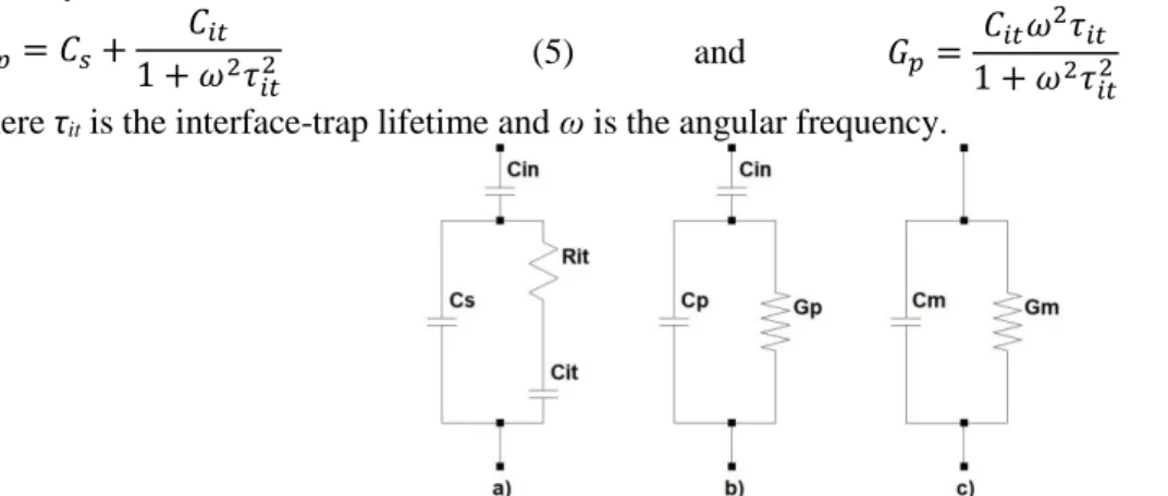
Figure 1.6 - Equivalent MIS circuits for conductance measurements: a) including interface-trap effect;
b) simplified circuit of a); c) device’s measured circuit. ... 5
Figure 2.1 – Experimental planning for the used CIGS pieces. Each CIGS piece was divided into four
samples. The CIGS A is to compare different types of depositions mostly with Al2O3 (dark blue)
and Si3Nx (light blue). The CIGS B aims to compare the same deposition technique (PECVD)
with the same material SiOx (purple) at different depostion conditions, namely different
temperatures and deposition frequencies. A - CdS and B - CdS (red) represent the reference samples for each CIGS piece. The layers are not at scale. ... 8
Figure 2.2 - HCl etch of CdS and subsequent insulator deposition. The layers are not at scale. ... 8 Figure 2.3 Mask used in the aluminium thermal evaporation. Holes with three diameters: 1 mm, 2 mm
and 3 mm. ... 9
Figure 2.4 a) Scheme of MIS structure: SLG/Mo/CIGS/insulator/Al. The molybdenum thickness is
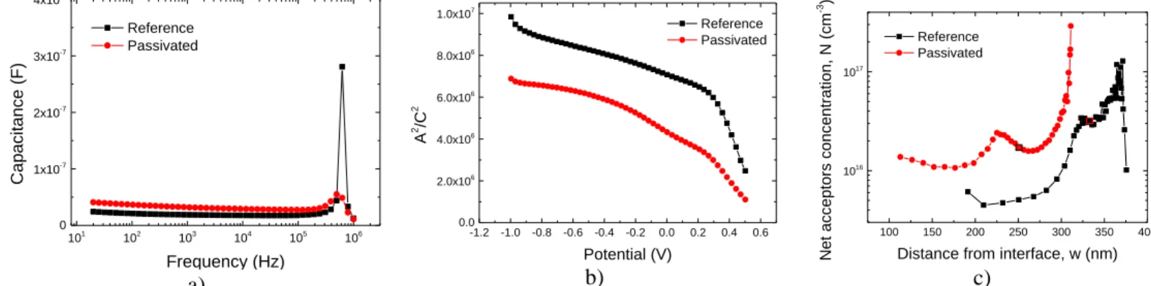
350 nm, the CIGS is 2 µm, the insulator 50 nm and the aluminium layer 400 nm (bilayer of 200 nm each). The image is not at scale. b) SEM cross-section of sample A – Al2O3 – S... 9 Figure 2.5 - Measurements of reference and passivated cell: a) C-f curve; b) Mott-Schottky curve and
c) N-w curve ... 11
Figure 3.1 Raman spectra of CIGS A in the left side and CIGS B in the right side. Each curve
represents different spots in the same sample: a) A - CdS; b) B - CdS; c) A - Al2O3 - S; d) B -
SiOx - 300 ºC; e) A - Si3Nx; f) B - SiOx - 150 ºC, HF; g) A - Al2O3 - ALD and h) B - SiOx - 150
ºC, LF. ... 14
Figure 3.2 Reference sample’s X-ray spectrum of CIGS A with Mo, Al, CdS and CuInSe2 crystalline
planes identified. ... 16
Figure 3.3 – Photoluminescence spectra of: a) CIGS piece A samples. b) CIGS piece B samples. .... 17 Figure 3.4 – Minority carriers’ lifetime of: a) All samples together including the reference samples;
b) Only samples with insulator deposition without the reference samples. ... 18
Figure 3.5 - Representative sample with MIS structures having several metal diameters, namely 1
mm, 2 mm and 3 mm. ... 19
Figure 3.6 – MIS structures using a qualitatively three-degree comparison: good (green), mixed
(yellow) and bad (red). CIGS A in the left side and CIGS B in the right side. A) A – CdS; b) A- Al2O3 – S; c) B - SiOx - 300 ºC; d) A - Si3Nx; e) B - SiOx - 150 ºC, HF; f) A - Al2O3 - ALD; and
g) B - SiOx - 150 ºC, LF... 21 Figure 3.7 - Shift in C-V curve due to fixed insulator charges in a p-type semiconductor. a) Positive
insulator charges effect; b) Negative insulator charges effect. Adapted from [39]. ... 23
Figure 3.8 - Representative C-V curve. Sample B – SiOx – 150 ºC, LF. MIS with 2 mm. ... 24 Figure 3.9 - Representative Vfb calculation through the graphical method. Sample B – SiOx – 150 ºC,
Insulator materials for electrical passivation of thin film solar cells
xvi Figure 3.10 - C-V representative curve of sample B – SiOx – 150 ºC, LF. MIS with 2 mm. ... 26 Figure 6.1 Raman spectra with different focus point of CIGS A in the left side and CIGS B in the
right side. Each graph represents: a) B – CdS; b) B - SiOx - 300 ºC; c) A - Si3Nx - 150 ºC, HF; d)
B - SiOx - 150 ºC, HF; e) A - Al2O3 - ALD and f) B - SiOx - 150 ºC, LF. The curves with low
peak intensities are out of focus. ... 36
Figure 6.2 Raman spectra of: a) Before CdS removal and b) After CdS removal. ... 36 Figure 6.3 X-ray diffraction spectra of: a) A - CdS; b) B - CdS; c) A - Al2O3 - S; d) B - SiOx - 300 ºC;
e) A - Si3Nx; f) B - SiOx - 150 ºC, HF; g) A - Al2O3 - ALD; h) B - SiOx - 150 ºC, LF and i) all
samples together. ... 38
Figure 6.4 - X-ray diffraction spectra zoom of the main CIGS peak (112). a) A - CdS, A - Al2O3 - S,
A - Si3Nx and A - Al2O3 – ALD samples; b) B - CdS, B - SiOx - 300 ºC, B - SiOx - 150 ºC, HF
and B - SiOx - 150 ºC, LF samples. ... 39 Figure 6.5 - Location of the fixed insulator charges (example of positive charges) and the density of
interface defects in the CIGS/insulator interface. Adapted from [40]. ... 39
Figure 6.6 - Ideal MIS C-V curves of a p-type semiconductor: (a) Low frequency; (b) Intermediate
frequency; (c) High frequency; (d) High freequency with fast-sweep (deep depletion). Flat-band voltage of 0V is assumed. Adapted from [40]. ... 40
Figure 6.7 - Band diagram of a MIS with a p-type semiconductor. a) Ideal MIS in flat-band; b) MIS
xvii
List of tables
Table 1 – Sample’s names used hereafter, considering the deposition used and the respective CIGS
piece. ... 7
Table 2 - Representative experimental planning of the AUTOLAB system and LCR comparisons. .. 12 Table 3 - Comparison between Raman spectroscopy and Photoluminescence measurements using a
qualitatively three-degree comparison: good, mixed and bad. ... 19
Table 4 - Comparison between the samples, taking into account the metal diameter using the
percentage of non-shunted structures and qualitatively three-degree overall comparison: good (green), mixed (yellow) and bad (red). ... 22
Table 5 – Cin average and standard deviation values of each diameter for each sample. ... 24 Table 6 – Vfb average and standard deviation values of each diameter for each sample. ... 25 Table 7 – Qf values taking into account the average Cin and Vfb calculated before. The red samples
have negative charges in the insulator. ... 25
Table 8 - Dit average and standard deviation values of each diameter for each sample. ... 27 Table 9 - Summary of all used techniques. Qualitatively three-degree overall comparison: good,
mixed and bad. The Qf measurement has different colours due to not be possible to do a
xix
Symbols
Symbol
Name
Unit
A
Area cm2Al
AluminiumAl
2O
x/Al
2O
3 Aluminium oxidea-Si
Amorphous SiliconC
Capacitance FCdS
Cadmium SulphideCdTe
Cadmium TellurideC
fb Flat-band capacitance FC
in Insulator capacitance FC
it Interface-trap capacitance FC
m Measured capacitance FC
p Frequency-dependent capacitance FC
s Semiconductor capacitance FCu
CopperD
it Density of interface defects eV-1cm-2E
C Conduction band eVE
F Fermi level eVE
g Energy bandgap eVE
V Valence band eVf
frequency HzFF
Fill factor %G
Conductance SGa
GalliumGaAs
Gallium ArsenideG
m Measured conductance SG
p Frequency-dependent conductance SH
2O
Hydrogen oxideH
2Se
Hydrogen selenideHCl
Hydrochloric acidHfO
2 Hafnium dioxideIn
IndiumJ
Current density A/m2J
0 Saturation current density A/m2J
M Maximum current density A/m2J
sc Short-circuit current density A/m2Insulator materials for electrical passivation of thin film solar cells
xx
L
n carrier diffusion length µmMo
Molybdenummpp
Maximum power point Wn
Ideality factor %N
Net acceptors concentration cm-3N
2 NitrogenN
2O
Nitrous oxideNH
3 AmmoniaNi
NickelP
inc Incident power Wq
Elementary charge CQ
f Fixed insulator charges cm-2Q
m Mobile ionic charges cm-2Q
ot Insulator trapped charges cm-2R
Resistance ΩR
it Interface-trap resistance ΩR
s Series resistance Ω/cm2R
sh Parallel resistance Ω/cm2Se
SeleniumSi
SiliconSi
3N
x/Si
3N
4 Silicon nitrideSiH
4-5 SilaneSiO
x/SiO
2 Silicon oxideT
Temperature KTiO
2 Titanium oxideV
Voltage VV
bias Supply voltage VV
D Applied voltage across the diode VV
fb Flat-band voltage VV
G Applied voltage VV
M Maximum voltage VV
oc Open-circuit voltage VV
RMS Root mean square voltage Vw
Distance from interface nmX
Reactance ΩX
c Capacitive reactance ΩZ
Impedance Ωxxi
Z''
Impedance imaginary part ΩZnO
Zinc oxideZnO:Al
Aluminium doped zinc oxideZnS
Zinc sulphideΔV
Voltage shift Vη
Power conversion efficiency %τ
it Interface-trap lifetime sφ
MS Metal-semiconductor work function difference Vxxiii
Acronyms
ALD
Atomic layer depositionCGS
Copper Gallium SelenideCIGS
Copper Indium Gallium Diselenide, Cu(In,Ga)Se2CIS
Copper Indium SelenideCPE
Constant Phase ElementCVD
Chemical vapour depositionDC
Direct currentHF
High frequencyINL
International Iberian Nanotechnology Laboratoryi-ZnO
intrinsic Zinc oxideLF
Low frequencyMIS
Metal-Insulator-SemiconductorOVC
Ordered Vacancy CompoundPECVD
Plasma-enhanced chemical vapour depositionPERC
Passivated emitter and rear cellPL
PhotoluminescenceRF
Radio frequencySEM
Scanning electron microscopySLG
Soda-lime-glassTMA
Trimethyl aluminiumTRPL
Time-resolved photoluminescenceXRD
X-ray diffractionYAG
Yttrium Aluminium Garnetxxv
Motivation and Objectives
For some time now, burning fossil fuels has been humanity’s main source of energy. Nonetheless, the environmental and limited availability issues related to this kind of source are pushing humanity to use other types of energy sources, such as the renewable ones. Environmental friendly technologies have the potential to provide long-term energy solutions together with a sustainable future. One of these tech-nologies is photovoltaics. Taking into account that the sun is, in practical turns, an “unlimited” source, humanity should take the maximum possible advantage of this technology. Photovoltaics are based on the conversion of solar radiation, i.e. photons, into an electrical current that can be used externally. The power conversion efficiency of a solar cell is defined as the ratio of electrical power delivered to the solar power, via light, reaching the solar cell [1]. In order for photovoltaics to be mass deployed at a world-wide level, the solar modules production cost should lower, whereas the electrical performance has to increase [2]. Photovoltaics technology has so much potential, that if the whole global electricity demand would be covered exclusively by solar modules, the total land area needed for light collection would only be approximately 360 000 km2 of desert area, the equivalent of slightly more than 1 % of
Sahara Desert [3,4].
Currently, a considerable amount of research on solar cells is being performed in order to: i) decrease the amount of material usage; ii) increase the solar cells electrical performance. Thin film solar cells are the most proficient technology to increase the electrical performance with high electricity gen-eration at competitive costs while at the same time preserving resources for future gengen-erations due to its high electrical performance and low-material usage [5]. Presently, three major thin film technologies are commercialized: amorphous silicon (a-Si), cadmium telluride (CdTe) and Cu(In,Ga)Se2 (CIGS) with
world-record power conversion efficiency values of 14 %, 22.1 % and 22.8 % respectively [6,7]. Alt-hough the CIGS laboratory cells have higher values of power conversion efficiency than multi-crystal-line Si (21.3 %), CIGS modules have power conversion efficiency values of 19.2 %, a value lower than the one of multi-crystalline modules which is currently at 19.9 % [6]. However, the silicon solar cells production cost per Watt is higher than CIGS and with the power conversion efficiency values of CIGS increasing, the costs continues to drop at a faster pace than the one of silicon [8]. Hence, it is predictable that in the near future, CIGS solar cells will be even more vastly used at a world-wide level.
The recombination losses at the CIGS solar cell interfaces are one of the most currently studied issues since by reducing these losses, the solar cell electrical performance can further improve. An in-novative solution is to use a passivation layer made of an insulator placed at the interfaces to reduce the recombination losses, hence increasing the electrical performance. This action, was one of the break-through discoveries that was done in silicon and that still is to be done in CIGS technology [2].
Due to the importance of developing passivation layers for CIGS technology, the work developed in this thesis is focused on the study of the effects of the passivation material and on the best deposition conditions to be used as a passivation layer. Insulator layers, such as, SiO2, Al2O3 and Si3N4, were tested
as the passivation material. Several characterization techniques were performed in order to allow us to identify which deposition conditions are capable of optimizing the passivation effects on the CIGS ab-sorber while maintaining the CIGS surface as pristine as possible. Raman scattering and X-ray diffrac-tion were used for the study of the possible CIGS damage due to the insulator deposidiffrac-tion. Metal-Insula-tor-Semiconductor (MIS) structures were made on CIGS absorber layers with aluminium as the top metal contact for electrical testing. The main thesis objective is the identification of the key parameters that will allow to choose an insulator material among several candidates capable of passivating the CIGS interfaces.
1
1
Introduction
1.1. Solar cell single-diode model
The current density-voltage (J-V) curve, presented in Figure 1.1 a), is one of the most important features of solar cells. Moreover, under light conditions and using the correct model, it is possible to extract figures of merit characteristic of solar cells, being the most important ones the short-circuit cur-rent density (Jsc), the open-circuit voltage (Voc) and the fill factor (FF), which in turn are used to estimate
the power conversion efficiency (η) of a solar cell device, defined by [9]: 𝜂 =𝐽𝑀𝑉𝑀
𝑃𝑖𝑛𝑐
=𝐽𝑆𝐶𝑉𝑂𝐶𝐹𝐹 𝑃𝑖𝑛𝑐
(1)
where JM is the maximum current density, VM is the maximum voltage and Pinc is the incident power. In Figure 1.1 a), Rsh is the parallel resistance and Rs is the series resistance. It is also shown how some of the solar cells figures of merit are extracted: Voc corresponds to the value of the voltage when the current density is equal to zero, Jsc is the value of current density when the voltage is zero, the fill factor (FF) is the ratio between the maximum generated power divided by 𝐽𝑠𝑐× 𝑉𝑜𝑐. The maximum power point (mpp), is the maximum voltage VM in Figure 1.1 a), (compared to Voc) multiplied by the maximum current density JM in Figure 1.1 a), (compared to Jsc) [10].
There are several models to electrically represent a solar cell. In CIGS solar cells the most used one is the “single-diode model” represented in Figure 1.1 b) [12].
a) b)
Figure 1.1 – a) Current-voltage curve characteristics of a solar cell under light. Adapted from [11].; b)
One-diode circuit model.
A single junction solar cell is a device based on a p-n junction, behaving in the same way as a diode. The typical equation describing this model, is [9,13]:
𝐽 = 𝑗0[exp ( 𝑞𝑉𝐷
𝑛𝑘𝑇) − 1] (2)
Where 𝐽 is the current density, 𝑗0 the saturation current density, 𝑞 the elementary charge, 𝑉𝐷 the applied voltage across the diode, 𝑛 the the ideality factor for a diode, 𝑘 the Boltzmann’s constant and 𝑇 the temperature. In a more realistic way, the cell should be presented with losses taking into account the series resistance and the parallel resistance (or shunt resistance as it is shown in Figure 1.1 b)), mathe-matically defined by:
𝐽 = 𝑗0[exp ( 𝑞𝑉𝐷− 𝑞𝑗𝑅𝑠 𝑛𝑘𝑇 ) − 1] + 𝑉𝐷− 𝑗𝑅𝑠 𝑅𝑠ℎ (3)
Insulator materials for electrical passivation of thin film solar cells
2
1.2. Cu(In,Ga)Se
2(CIGS) based solar cells
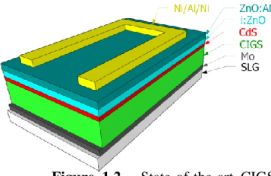
The conventional CIGS solar cell structure is shown in Figure 1.2. The solar cell is constituted by the following layers (from bottom to top):
- SLG (soda-lime-glass) substrate as the mechani-cal support of the entire cell structure. It is gener-ally used due to the fact that it is cheap, roughly planar and it is widely available in several sizes. Its sodium content is beneficial for the CIGS elec-trical performance, diffusing into the CIGS layer through the molybdenum layer [14].
- Molybdenum (Mo) bilayer as the rear electrical contact. One layer to form a good adhesion with the SLG and the other to form an ohmic contact with the CIGS layer while keeping a high value of electrical conductivity.
- Cu(In,Ga)Se2 (CIGS), a p-type semiconductor, as the absorber layer, being discussed later.
- CdS, a n-type semiconductor, with a direct bandgap of 2.4-2.5 eV, buffer layer that should be able to: i) transmit most of the incoming light; ii) form a high-quality p-n heterojunction in-cluding a good energy band alignment match-up [15]; and, iii) to achieve low interface re-combination losses.
- Window bilayer. The first, consisting of a very thin layer, below 100 nm, transparent conduc-tive oxide, intrinsic ZnO (i-ZnO) as the interface of the window and buffer layer, creating a favourable band alignment, low interfacial losses and high resistance (preventing conductive paths from the back contact). The second layer, a doped ZnO:Al layer with low resistance, high conductivity and allowing the transmission of the incoming radiation.
- Top contact made of Ni/Al/Ni.
1.2.1
Material and advantages
The CIGS compound belongs to the group of the chalcogenides solar cells. The chalcogenides, refers to all chemical compounds with at least one chalcogen anion from
the group 16 of the period table (group IV). This anion, in the CIGS case, refers to Se (selenium). One of the chalcogenides groups, are the chalco-pyrite solar cells. All chalcochalco-pyrites have tetragonal crystal structures as it is shown in Figure 1.3.
The chalcopyrites, many of them semiconductors, consists of ele-ments of groups I, III and IV, being also called I-III-IV semiconductors or ternary semiconductors. One of the chalcopyrites used for solar cells is a compound consisting of a solid mixture of copper indium diselenide (CuInSe2, CIS) and copper gallium diselenide (CuGaSe2, CGS). This
compound is the copper indium gallium diselenide [Cu(InxGa1-x)Se2,
CIGS], where x can vary between 0 and 1.
The CIGS compound is a p-type and direct bandgap semiconduc-tor, with an excellent long-term stability [17]. It has high absorption co-efficient values, up to 105 cm-1. The high absorption coefficient values are
a huge advantage comparing to other solar cells absorbers, like crystalline silicon with an indirect energy bandgap and an absorption coefficient of 103 cm-1. This means that the silicon solar cells must be thicker,
around 200 µm, whereas CIGS solar cells only need a few micrometres (1-3 µm) for absorbing the same amount of the incoming light with energy values above the bandgap energy. The electron diffusion length is low but in the order of the used thicknesses, from 0.75 µm to 1.5 µm [18] which is a value of importance for the passivation layer.
Figure 1.2 - State-of-the-art CIGS
solar cell structure. The incoming light is reaching the solar cell on top of the shown structure. The layers are not at scale.
Figure 1.3 - Typical
structure of CIGS chalcopyrite. The indium atoms can be re-placed by gallium. Adapted from [16].
3
Another interesting CIGS compound feature is its self-doping nature. This self-doping nature and the p-type property is directly related with Cu vacancies [19].
The properties of the CIGS compound are determined mostly by its Cu content: with low copper concentration (Cu-poor CIGS), which is defined by [Cu]/([Ga]+[In]) < 1, in other words, the concentra-tion of copper is lower than Ga and In together. On the other hand, higher copper concentraconcentra-tion (Cu-rich CIGS), defined by [Cu]/([Ga]+[In]) > 1. Cu-(Cu-rich CIGS has good crystalline properties (big grains), nonetheless its electrical performance is weaker due to lower levels of p-type doping and increased appearance of secondary phases of Cu2-xSe. On the other hand, Cu-poor CIGS has poor crystalline
prop-erties, but better electrical performance, being preferential for solar cells [9,20].
Another of the CIGS advantages is the possibility to engineer the bandgap and to create a quasi-electric field, by adjusting the amount of gallium content, i.e. by the elemental substitution of In by Ga, making the energy bandgap mutable from 1.02 eV to 1.69 eV.
1.2.2
State of the art
The Shockley–Queisser limit of power conversion efficiency, i.e. the theoretical limit, for the CIGS solar cells is around 33 %, making them one of the most studied solar cells at the present time [1].
The history of CIGS started in 1975, when Bell laboratories scientists achieved a power conver-sion efficiency of 12 % with CdS on top of CuInSe2 crystals [21,22]. Furthermore, different types of
depositions processes (co-evaporation where Cu, In and Se are deposited individually; deposition-reac-tion process using Cu and In as metallic precursors together with H2Se) were developed to explore the
best deposition method in terms of electrical performance and industrialization [22]. In 1994, National Renewable Energy Laboratories (NREL) invented the so called three-stage process [23]. The three-stage process, was so successful, providing the basis for the solar cells with power conversion efficiency val-ues above 20 % that is still the most used deposition process for laboratory solar cells.
Research teams have been studying alkali elements effects on the absorber layer since the 1980s with Boeing Aerospace Company being the first [24]. Currently, alkali elements effects on CIGS, is a continuous research topic [14]. Similarly, by 1980, B.J. Stanbery and co-workers implemented mono-lithic integration in the solar-cell stack for module production [24,25]. Another achievement for the CIGS solar cells, was the discovery of the bandgap tuning with the Ga grading. The full comprehension of all the defects in the CIGS absorber layer, how they affect the performance of the solar cell and the solution for those problems is yet not entirely understood. Nevertheless, nowadays the record CIGS solar cell belongs to ZSW with power conversion efficiency of 22.8 % [7]. These solar cells were made in a state-of-the-art laboratory using the co-evaporation method. It is believed that with improvements in interface passivation this efficiency can be largely increased in the next few years [26,27].
1.3. Passivation
The major electrical losses in CIGS solar cells, nowadays, are bulk and interface recombination, which makes them the main performance drawbacks [26].
The common method to reduce the rear surface recombination in state-of-the-art solar cells is by Ga grading [28]. Such grading creates a quasi-electric field that repels the minority carriers from the rear surface [29]. However, the Ga gradient method has several disadvantages. A too low [Ga]/([Ga]+[In]) ratio leads to unsuited band alignment and a to high ratio leads to an increase in the CIGS defect density [11]. With an increase in material grading, potential fluctuations also increase, which decreases the solar cell electrical performance [30].
The interface recombination can be largely supressed by passivating the interfaces. Two types of passivation can be defined: i) chemical passivation, happening when the density of active defects is effectively reduced in the CIGS surface; and ii) field-effect passivation (coulomb repulsion), when the charges inside the passivation layer creates a field effect that repel the carries or enhance the surface inversion (positive charges). When the passivation occurs in the rear interface, another type of effect can happen, an optical effect, which consists in reflecting the light from the passivation layer, thus in-creasing the path light inside the absorber layer [31]. The use of a passivation layer, jointly with
nano-Insulator materials for electrical passivation of thin film solar cells
4
sized point contacts, is also important to decrease even more the CIGS absorber layer thickness from few micrometres to hundreds of nanometres [18,29].
The idea of nano-sized local point contacts came from silicon solar cells, where this kind of struc-ture is used to increase the Voc, thus the efficiency. The so called PERC structure (Passivated emitter
and rear cell) is described by Green in [2], depicted in Figure 1.4 i), with the following advantages: reduction of rear surface recombination by a combination of an insulator surface passivation and reduced metal/semiconductor contact area, with simultaneously increased rear surface refection. Nevertheless, to bring this feature to CIGS solar cells, both the minority and majority carrier diffusion lengths have to be well known, that are orders of magnitude lower than in the Si solar cells. In CIGS solar cells, to do point contacts, they must have an appropriate spacing and avoid minority carrier losses, as it is shown in Figure 1.4 ii).
i) ii)
Figure 1.4 – i) First diagram of PERC structure [2]. ii) Schematic representation of the rear of (a) a
p-type Si solar cell with a surface passivation stack and micron-sized local point contacts and (b) a CIGS solar cell with a surface passivation stack and nano-sized local point contacts. Also, typical base/absorber thickness, mi-nority carrier diffusion length (Ln), contact opening diameter and distance between contact openings are
speci-fied [18].
Nowadays, it is common practice to use Al2O3 as an insulator deposited by ALD in silicon solar
cells technology [32,33]. Other materials are being the focus of many research teams like TiO2 [34] and
ZnS [35,36]. Possible candidates, such as, HfO2, SiO2 and Si3N4 are also referred in literature [24]. The
thickness of the passivation layer and the deposition conditions are also a matter of study to reach the best passivation possible, integration of other advanced light trapping techniques and studying other candidates for the passivation layer [13]. The study of other types of passivation layers, as well as, the most suitable deposition conditions are the purpose of this thesis.
1.4. MIS structures
Metal-Insulator-Semiconductor (MIS) structures are of special importance in the field of elec-tronics and can be used in optoelecelec-tronics to extract relevant device parameters. Particularly, performing MIS measurements, it is possible to study the electronic properties of the insulator-semiconductor inter-face. More precisely, with MIS measurements, it is possible to identify the interface density of de-fects/traps. Regarding the study of different types of passivation, the density of interface defects (Dit)
related to the already mentioned chemical passivation, is accomplished by performing C-G-f measure-ments, whereas the number of fixed insulator charges estimation (Qf) related to the field-effect
pas-sivation, is reached through C-V-f measurements. In order to do the different measurements, it is nec-essary to understand the different MIS conditions in the C-V curve, namely the accumulation, the de-pletion and inversion regions, as it is shown in Figure 6.6 of Annexes.
1.4.1
Fixed insulator charges (Q
f)
To extract Qf it is necessary to perform C-V measurements, at selected frequencies, to understand
the depletion/weak-inversion transition region. The Qf is calculated by [22,37]:
𝑄𝑓 =
𝐶𝑖𝑛(𝜙𝑀𝑆− 𝑉𝑓𝑏)
5
where ϕMS is the work function difference between the metal and the semiconductor, A is the metal surface area, q is the elementary charge, Vfb is the flat-band voltage, that will be explained in more detail later and Cin is the insulator capacitance value extracted in strong accumulation condition of a C-V curve.
The flat-band voltage is of special interest in this calcula-tion, being the voltage required to make the energy bands to be flat, when a charge is present inside the insulator, as shown in
Figure 6.7 of Annexes.
Several methods are presented by Piskorski et al. [38] to calculate the Vfb. In this work we used the graphical method, also
known as the [(Cin/Cm)2-1](VG) method, shown in Figure 1.5.
1.4.2
Density of interface defects (D
it)
To extract Dit, several methods are reported in the literature for silicon and GaAs devices [37].
The Conductance Method introduced by Nicollian and Brews [22,39], is used in this thesis. It is the most accurate density of interface defects extraction method and insensitive to parasitic effects [39,40]. The Conductance Method is based on the equivalent circuit, presented in Figure 1.6 a), where
Cin is the insulator capacitance, Cs is the semiconductor depletion layer capacitance, Cit and Rit are the capacitance and resistance associated with the interface-traps. The parallel circuit in Figure 1.6 a) can be converted into a frequency-dependent capacitance Cp and a frequency-dependent conductance Gp,as shown in Figure 1.6 b). In Figure 1.6 c), Cm is the measured capacitance and Gm is the measured con-ductance which is the circuit that the measuring equipment uses. The relations between Cp and Gp are given by [40]: 𝐶𝑝= 𝐶𝑠+ 𝐶𝑖𝑡 1 + 𝜔2𝜏 𝑖𝑡2 (5) and 𝐺𝑝= 𝐶𝑖𝑡𝜔2𝜏𝑖𝑡 1 + 𝜔2𝜏 𝑖𝑡2 (6) where τit is the interface-trap lifetime and ω is the angular frequency.
Figure 1.6 - Equivalent MIS circuits for conductance measurements: a) including interface-trap effect; b)
simplified circuit of a); c) device’s measured circuit.
Plotting (Gp/ω) against the frequencies (f) will yield a maximum in the energy loss mechanism.
The maximum gives direct information about the density of interface defects [37]. The relation is given by [22,41]: 𝐷𝑖𝑡 = ( 2.5 𝐴 × 𝑞) ( 𝐺𝑝 𝜔)𝑚𝑎𝑥 (7) where (𝐺𝑝 𝜔) is calculated accordingly by [22,39]: (𝐺𝑝 𝜔) = 𝜔𝐺𝑚𝐶𝑖𝑛2 𝐺𝑚2 + 𝜔2(𝐶𝑖𝑛− 𝐶𝑚)2 (8)
where Cin being the measured capacitance in strong accumulation.
Figure 1.5 - Vfb is extrapolated
from the linear part of [(Cin/Cm)2-1](VG)
7
2
Materials and methods
The main focus of this work is the study of the effects of several insulators types, namely alumin-ium oxide (Al2Ox), silicon nitride (Si3Nx) and silicon oxide (SiOx), on the CIGS interface properties.
Taking into account that only two 5x5 cm2 SLG/Mo/CIGS/CdS samples were available, a carefully
experimental planning was needed to account for the differences between the insulators types and dep-osition methods. It is necessary to understand that the two samples of material were made in the same day and the same way, however, due to the inhomogeneous CIGS deposition, differences between them might not make possible comparisons between the two CIGS pieces. Hence, the experimental planning had also to account for sample inhomogeneity by having a reference in each of the two samples.
The samples were made of soda-lime glass substrate (2 mm), molybdenum back contact (350 nm), Cu(In1-x,Gax)Se2 as absorber layer (2 µm) and cadmium selenide (CdS) (70 nm) on top of it to
prevent air exposure to the CIGS during handling [42,43]. The Mo deposition was carried out by DC-sputtering and the CdS deposition was done by chemical bath deposition. The CIGS deposition occurred in Uppsala University by co-evaporation, accordingly to Ångström solar cell baseline, with a thickness of approximately 2 µm. There is a Ga gradient from [Ga]/([Ga]+[In]) = 0.25 at the front contact to 0.65 toward the rear contact, which corresponds in a rear contact bandgap energy of 1.14 eV to 1.38 eV in the front contact [44].
The following section presents the experimental planning to understand the succeeding results and discussion in the next chapter.
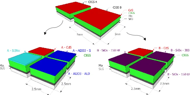
2.1. Experimental planning
Two samples with 5x5 cm2 were cut, using a pen with a diamond point, into four smaller samples
of 2.5x2.5 cm2 as it is shown in Figure 2.1.
In order to a better understanding of each sample name, Table 1 shows the names used hereafter.
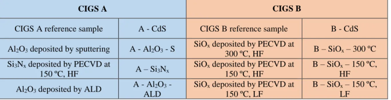
Table 1 – Sample’s names used hereafter, considering the deposition used and the respective CIGS piece.
CIGS A CIGS B
CIGS A reference sample A - CdS CIGS B reference sample B - CdS Al2O3 deposited by sputtering A - Al2O3 - S
SiOx deposited by PECVD at
300 ºC, HF B – SiOx – 300 ºC Si3Nx deposited by PECVD at
150 ºC, HF A – Si3Nx
SiOx deposited by PECVD at
150 ºC, HF B – SiOx – 150 ºC, HF Al2O3 deposited by ALD A - Al2O3 - ALD
SiOx deposited by PECVD at
150 ºC, LF
B – SiOx – 150 ºC,
LF
On the first CIGS piece (CIGS A), the main focus was the Al2O3, which is a well-known
pas-sivation layer for silicon solar cells. Two different deposition techniques were used in order to under-stand which one is more suitable: sputtering and atomic layer deposition (ALD). Also, in this CIGS piece, a sample of Si3Nx was deposited to comprehend the differences between Si3Nx and Al2O3. In the
second CIGS piece (CIGS B), the same technique (PECVD) and the same material (SiOx) were used to
reach the ideal deposition conditions. It is noted that in both CIGS pieces, one sample of SLG/Mo/CIGS/CdS remained intact, to serve as the reference for each CIGS piece. The planning rep-resentation is shown in Figure 2.1.
Insulator materials for electrical passivation of thin film solar cells
8
Figure 2.1 – Experimental planning for the used CIGS pieces. Each CIGS piece was divided into four
samples. The CIGS A is to compare different types of depositions mostly with Al2O3 (dark blue) and Si3Nx (light
blue). The CIGS B aims to compare the same deposition technique (PECVD) with the same material SiOx
(purple) at different depostion conditions, namely different temperatures and deposition frequencies. A - CdS and B - CdS (red) represent the reference samples for each CIGS piece. The layers are not at scale.
2.2. MIS fabrication and depositions techniques
This section aims to explain the insulator deposition, since it was the only fabrication step done in this work. It is necessary to understand that the CIGS’s air exposure is a degrading process which severally affects the CIGS surface. Thus, by doing a CdS coverage, the CIGS surface will remain pris-tine, even after the CdS removal. However, the CdS removal should be a fast process in order to avoid the CIGS air exposure.
Before the insulator deposition, the CdS removal was necessary, as it is shown in Figure 2.2. In order to do the CdS removal, 10 % (w/w) HCl was used during 2 min to etch the CdS layer [45]. Sub-sequently, the sample was taken to the deposition tools in a matter of seconds to avoid CIGS air expo-sure.
Figure 2.2 - HCl etch of CdS and subsequent insulator deposition. The layers are not at scale.
Several insulator materials with a thickness of 50 nm were deposited using different techniques: i) Aluminium oxide (Al2O3) by sputtering, using a Metallization Singulus Sputtering tool
(Timaris FTM). The deposition was carried out by a standard INL recipe to deposit specifically 50 nm. The RF mode was used at 1500 W and argon injection with a flow of 200 sccm. The starting pressure was 7x10⁻⁸ mbar increasing with the argon injection,
9
increased, however, due to the proximity to the Al2O3 target, it can reach temperature
values as high as 200 ºC.
ii) Silicon nitride (Si3Nx) by Plasma Enhanced Chemical Vapour Deposition (PECVD),
using SPTS MPX CVD tool at 150 ºC, High Frequency (HF) of 13.56MHz, plasma power of 30 W and as precursor gases NH3, SiH4-5 and N2.
iii) Silicon oxide (SiOx) by PECVD, using the same tool at three different deposition
con-ditions: 300 ºC and 150 ºC, HF, plasma power of 30 W and as precursor gases N2O,
SiH4-5 and N2; 150 ºC, low frequency (LF) of 380kHz, plasma power of 60 W and the
same precursor gases.
iv) Aluminium oxide (Al2O3)by atomic layer deposition (ALD) was done in Uppsala
Uni-versity at 200 ºC, using as precursor gases Trimethyl aluminum (TMA) as aluminum source and H2O as oxygen source.
Another set of insulator depositions, with the same conditions as the ones describe before, were carried out in silicon substrates in order to evaluate the film thickness. The thickness measurement was done using a contact profilometer (KLA TENCOR P-16+). We reached the conclusion that all deposi-tion techniques accomplish thicknesses in the order of 50 nm corresponding to the required value.
To create the MIS structure, the metal aluminium layer front contact, was deposited at the Faculty of Science and Technology, New University of Lisbon. These contacts were done by thermal evapora-tion, with an initial pressure of 5x10⁻⁶ mbar, in two steps: 200 nm deposition thickness in each step, to
accomplish the desired 400 nm with the pattern shown in Figure 2.3:
Figure 2.3 Mask used in the aluminium thermal evaporation. Holes with three diameters: 1 mm, 2 mm
and 3 mm.
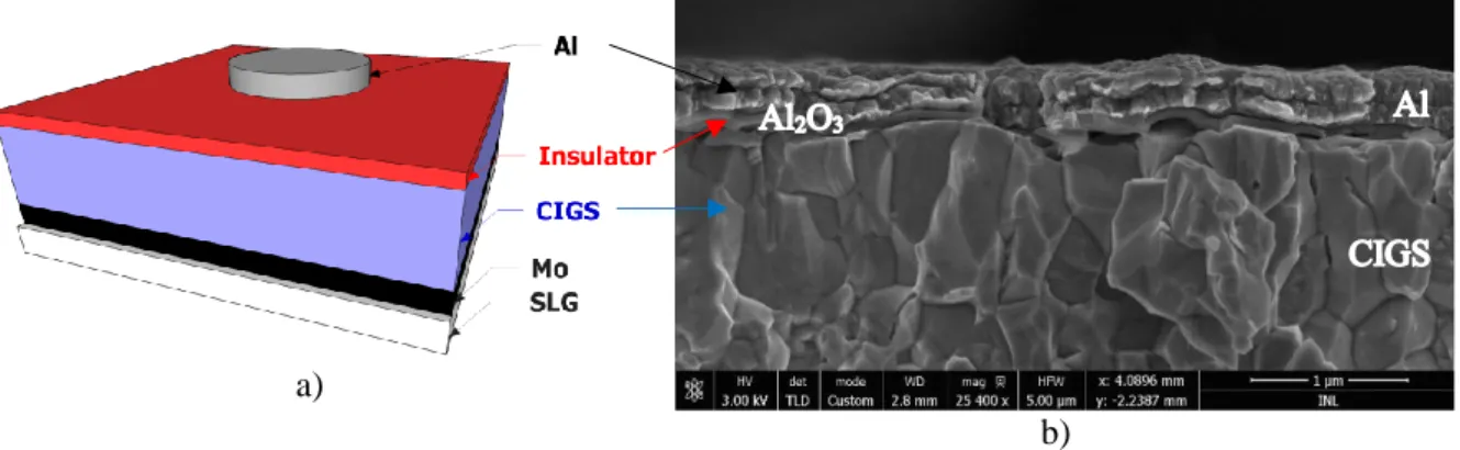
The final scheme of one MIS structure and a representative SEM cross-section are depicted in
Figure 2.4.
a)
b)
Figure 2.4 a) Scheme of MIS structure: SLG/Mo/CIGS/insulator/Al. The molybdenum thickness is 350
nm, the CIGS is 2 µm, the insulator 50 nm and the aluminium layer 400 nm (bilayer of 200 nm each). The image is not at scale. b) SEM cross-section of sample A – Al2O3 – S.
Insulator materials for electrical passivation of thin film solar cells
10
2.3. Characterization techniques
The CIGS surface characterization must be done to better understand the possible damage of each deposition and the electrical interface performance between the insulator and the CIGS after the depo-sition. Raman spectroscopy, x-ray diffraction, photoluminescence and time-resolved photolumines-cence analysis were performed to characterize the CIGS interface, thus the damage impinged by the insulator deposition. Electrical measurements were done to better understand the insulator/CIGS inter-face, namely if a low density of interface defects is accomplished.
Raman spectroscopy was done, using Confocal Raman Microscope 300 R (WiTec) with green laser (excitation wavelength of 532 nm), 1 mW of power and a Zeiss objective of 100x in the backscat-tering configuration.
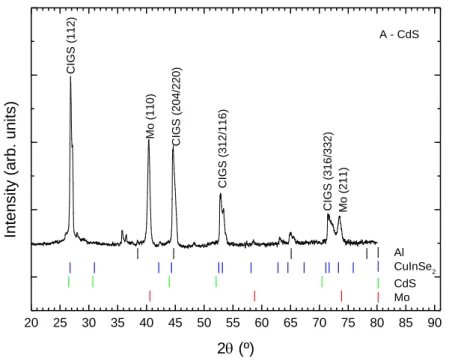
X-ray diffraction (XRD) was conducted using PANalytical’s diffractometer system XPERT-PRO with a cooper source Kα (wavelength 1.540598 Å), using Bragg-Brentano theta-2theta configuration.
Photoluminescence (PL) and Time-resolved photoluminescence (TRPL) were performed at IMEC in Belgium. It was used a YAG, class 3B laser with a 15kHz repetition rate and 1 ns pulse length with a beam spot of 3 mm and excitation wavelength of 532 nm. An average illumination intensity of 1 mW was used. TRPL was checked at the excitation wavelength that matched the PL peak in each case varying from 1090 to 1125 nm. In order to extract lifetime values, a common procedure is to use a second order fitting (bi-exponential decay model) which was the selected method used in this work.
Scanning electron microscopy (SEM) cross-section was carried out, using the NovaNanoSEM 650 tool with an acceleration voltage of 3kV.
The techniques used so far, were to study changes in the CIGS properties, more precisely in the interface with the insulator. From now on, Metal-Insulator-Semiconductor (MIS) measurements were done to study the electrical properties of the CIGS/insulator interface.
C-G-f measurements were done in Agilent E4890 A with 30 mV (VRMS), 0V in Vbias, 1m cable
correction and 10 iterations with a medium iteration time, from 20 Hz to 1 MHz. C-V-f measurements were done in the same tool with 30 mV (VRMS),a frequency of 10 kHz, 1 m cable correction and 10
iterations with medium iteration time with different Vbias ranges, depending on the samples and front
contact area.
Simulations of the MIS structure model were performed in the ZSimpWin 3.50 software. This software allowed for detection of shunted cells, as well as the appropriate fitting model for each working cell.
2.4. Electrical measurement tool
At the beginning of the master thesis, there was no electrical measurement tool and nobody in the group knew the electrical measurements know-how. Keeping in mind that the MIS measurements were needed, we start looking into de INL’s groups and we found that two tools were available to do the electrical measurements, namely the AUTOLAB system PGSTAT302N, henceforth called AUTOLAB, and the LCR Agilent E4890 A, hereafter called LCR. Despite the AUTOLAB been mostly used by chemistry users, it allows us to perform the measurements that we need. In order to study the both tools limitations, a considerable amount of experimental planning was done using solar cells. Initially, MIS structures were not used due to the fact that we did not know what to expect from the measurements. However, from the solar cells we knew very well the behaviour under certain conditions, therefore they were the perfect testbed.
The AUTOLAB was not designed to measure solar cells, however, this tool has the electrical measurements procedures already defined with the possibility to change the measurement parameters, namely the Vbias, the VRMS, the integration time, the frequency, among others. We began with a “dummy
cell” to serve as a test cell, in order to calibrate the device. After the test cell measurements, therefore the system calibration, we began to understand better the operation of the equipment. Subsequently, several measurements were carried out on passivated CIGS solar cells and on standard CIGS solar cells. Initially, we began with I-V curves under dark conditions and the obtained curves were not what we
11
expected. We started the measurements with crocodile clips, however due to the unexpected results, a change to BNC cables connected to micro positioners with tips were done and the I-V curves started looking as they should be. It is noted that in order to understand the functionality of the different cables, an experimental planning was done under the same conditions, only varying the parameter that we wanted, in this case, the change from crocodile clips to micro positioners with tips. More experimental planning was done, namely the experience of measuring the cells with and without light soaking done before the measurements, changing the integration times and number of cycles, changing the VRMS
val-ues, among others. Then, Mott-Schottky, as well as, C-f and N-w measurements were done as it is shown in Figure 2.5.
a) b) c)
Figure 2.5 - Measurements of reference and passivated cell: a) C-f curve; b) Mott-Schottky curve and c)
N-w curve
The outcomes started to be as expected, and a very well-defined procedure for Mott-Schottky measurements was established. The results were used as complementary measurements in a poster1
presentation and for a paper2 publication.
After several measurements, and as it is shown in Figure 2.5 a), the AUTOLAB had limitations at high values of frequency. Also, after C-V measurements performed to MIS structures, one realized that the equipment was not able to go below -2V and above 2V, thus C-V measurements were highly limited. The use of LCR device started, and comparisons between the two equipment were done.
By default, in the measurements, the LCR assumes the Cp-Rp parallel circuit. However, the
AU-TOLAB assumes the same equivalent circuit with a series resistance. This series resistance value should be inserted by the user and, consequently, it should be well known for each device under test. An exper-imental planning was done to compare several parameters, such as the series resistance change, the VRMS
change, and their influence on the results, as it is shown in Table 2.
1 P.M.P. Salomé, J.P. Teixeira, M.A.M. Cardoso, V. Fjällström, P.A. Fernandes, J.M.V. Cunha, M. Edoff,
N. Nicoara, J.P. Leitão, S. Sadewasser, “Analysis of waiting times between CIGS and CdS and in-diffusion of Na on the properties of Cu(In,Ga)Se2 materials and solar cells”, presented in 2017, April 17-21, MRS in Phoenix,
Arizona.
2 P.M.P. Salomé, Bart Vermang, R. Ribeiro-Andrade, J.P. Teixeira, J.M.V. Cunha, M. J. Mendes, S. Haque,
J. Borme, H. Aguas, E. Fortunato, R. Martins, J.C. González, J. P. Leitão, P.A. Fernandes, M. Edoff and S. Sa-dewasser, “Passivation of interfaces in thin film solar cells: understanding the effects of a nanostructured rear point contact layer”, submitted to Advanced Materials Interfaces.
101 102 103 104 105 106 0 1x10⁻⁷ 2x10⁻⁷ 3x10⁻⁷ 4x10⁻⁷ Capaci tance (F) Frequency (Hz) Reference Passivated -1.2 -1.0 -0.8 -0.6 -0.4 -0.2 0.0 0.2 0.4 0.6 0.0 2.0x10⁶ 4.0x10⁶ 6.0x10⁶ 8.0x10⁶ 1.0x10⁷ A 2 /C 2 Potential (V) Reference Passivated 100 150 200 250 300 350 400 1016 1017 Net acc eptors conc entration, N (cm -3 )
Distance from interface, w (nm)
Reference Passivated
Insulator materials for electrical passivation of thin film solar cells
12
Table 2 - Representative experimental planning of the AUTOLAB system and LCR comparisons.
After several tests in both AUTOLAB and LCR, we choose the LCR due to be the more accurate tool, with less parameters to change and, apparently, with less limitations. However, it had limitations too, at very low and vert high frequencies due to the cables configuration.
The measurements of the Gp/ω against the frequencies were initially quite complex as there was no experience in the group and the literature on the measurements conditions is very scarce. Experi-mental planning with silver ink on the front metal of the MIS structures and scribing of the MIS struc-tures were made in order to understand their influence on the measurements. Several tests were done until the final method to perform the electrical measurements was accomplished.
13
3 Results and Discussion
In this chapter, each result will be shown and discussed. Firstly, we need to take into consideration if the deposition of the insulator caused any damage to the CIGS, thus, in this case we will be taking conclusions about the deposition technique and the deposition conditions used. Then, it is needed to understand, even if the CIGS surface and bulk are not damaged, if electrically the structure is working well, in other words, if the insulator material is actually passivating the CIGS layer, keeping a good electrical performance.
First, to analyse the CIGS layer, namely possible CIGS surface damage or modification, due to the insulator deposition, Raman scattering was performed since it is a shallow measurement which al-lows us to identify surface changes. In order to understand if bulk CIGS damaging occurred as well, X-ray diffraction was done due to be a bulker measurement technique. As complementary techniques, photoluminescence was taken to study the CIGS defects and time-resolved photoluminescence was done to study the carrier’s lifetime.
Finally, with the MIS structures completed, to study the structure electrical performance, meas-urements were performed to reach the fixed insulator charges and the density of interface defects.
All techniques together, will allow us to reach the effects of the passivation layer to be used to-gether with the best deposition technique.
3.1.
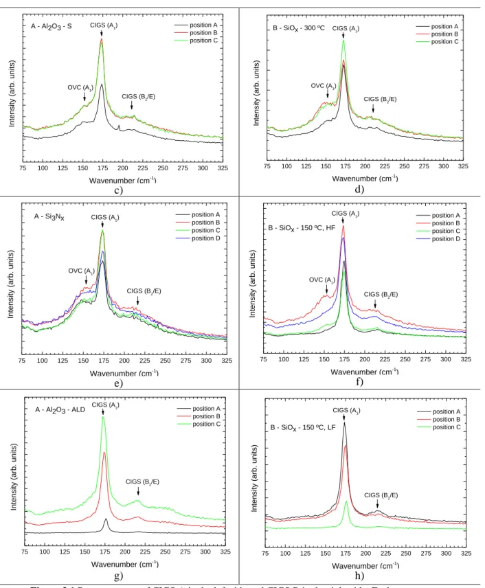
Raman spectroscopy
In this section, we aim to understand if the CIGS surface was modified or damaged, due to the CdS removal and/or due to the insulator deposition. Since the Raman technique is a shallow measure-ment, mostly surface variations are observed. Raman spectra for each sample are depicted in Figure
3.1. a) b) 75 100 125 150 175 200 225 250 275 300 325 CIGS (B2/E) CdS Int en sity (a rb . u nits) Wavenumber (cm-1 ) position A position B position C CIGS (A1) A - CdS 75 100 125 150 175 200 225 250 275 300 325 B - CdS Int en sity (a rb . u nits) Wavenumber (cm-1) position A position B position C CIGS (B2/E) CdS CIGS (A1)
Insulator materials for electrical passivation of thin film solar cells
14
c) d)
e) f)
g) h)
Figure 3.1 Raman spectra of CIGS A in the left side and CIGS B in the right side. Each curve represents
different spots in the same sample: a) A - CdS; b) B - CdS; c) A - Al2O3 - S; d) B - SiOx - 300 ºC; e) A - Si3Nx; f)
B - SiOx - 150 ºC, HF; g) A - Al2O3 - ALD and h) B - SiOx - 150 ºC, LF.
First, we measured the reference sample of the CIGS A, since the CIGS layer was pristine and only the CdS was deposited to serve as a protective layer, taking into consideration that the CdS depo-sition does not damage the CIGS layer. As it is shown in Figure 3.1 a), in the A – CdS sample, it is clearly visible the main CIGS peaks, namely the narrow CIGS A1 mode peak centred at 172 cm-1 [46],
and the broader CIGS B2/E modes peaks appearing between 210 cm-1 and 227 cm-1 [47]. Also, since
75 100 125 150 175 200 225 250 275 300 325 A - Al2O3 - S Int en sity (a rb . u nits) Wavenumber (cm-1) position A position B position C CIGS (A1) OVC (A1) CIGS (B2/E) 75 100 125 150 175 200 225 250 275 300 325 B - SiOx - 300 ºC Int en sity (a rb . u nits) Wavenumber (cm-1 ) position A position B position C CIGS (A1) OVC (A1) CIGS (B2/E) 75 100 125 150 175 200 225 250 275 300 325 A - Si3Nx Int en sity (a rb . u nits) Wavenumber (cm-1 ) position A position B position C position D CIGS (A1) OVC (A1) CIGS (B2/E) 75 100 125 150 175 200 225 250 275 300 325 B - SiOx - 150 ºC, HF Int en sity (a rb . u nits) Wavenumber (cm-1 ) position A position B position C position D CIGS (A1) OVC (A1) CIGS (B2/E) 75 100 125 150 175 200 225 250 275 300 325 Int en sity (a rb . u nits) Wavenumber (cm-1 ) position A position B position C CIGS (A1) CIGS (B2/E) A - Al2O3 - ALD 75 100 125 150 175 200 225 250 275 300 325 B - SiOx - 150 ºC, LF Int en sity (a rb . u nits) Wavenumber (cm-1) position A position B position C CIGS (A1) CIGS (B2/E)
![Figure 1.1 – a) Current-voltage curve characteristics of a solar cell under light. Adapted from [11].; b) One-diode circuit model](https://thumb-eu.123doks.com/thumbv2/123dok_br/15194243.1017246/27.892.114.789.378.811/figure-current-voltage-curve-characteristics-solar-adapted-circuit.webp)
![Figure 1.4 – i) First diagram of PERC structure [2]. ii) Schematic representation of the rear of (a) a p- p-type Si solar cell with a surface passivation stack and micron-sized local point contacts and (b) a CIGS solar cell](https://thumb-eu.123doks.com/thumbv2/123dok_br/15194243.1017246/30.892.171.715.328.490/figure-diagram-structure-schematic-representation-surface-passivation-contacts.webp)