Daniel Araújo Barros
Reflow Soldering in an Oxidant Atmosphere
Daniel Araújo Barros
R eflo w Solder ing in an Oxidant A tmospher e
Universidade do Minho
Escola de Engenharia
Master Thesis
Integrated Master in Materials Engineering
Work done under the guidance of
Professor José Carlos Fernandes Teixeira
Professor Delfim Fernandes Soares
Dr. José Ricardo Barros Alves
Daniel Araújo Barros
Reflow Soldering in an Oxidant Atmosphere
Universidade do Minho
A
CKNOWLEDGMENTSI would like to thank all the wonderful people that directly or indirectly helped and supported me to do this dissertation. It was a pleasure for me to work with all of them. First and foremost I would like to thank my advisors, Professor Delfim Soares and Professor José Carlos Teixeira for all the support, dedication, provided ideas and the time spent in this project.
I would like to especially thank my mentor at BOSCH Car Multimedia Dr. José Ricardo Barros Alves for the tremendous support and time spent in our meetings. Their ideas had a major influence on my work and to this dissertation.
I would like to thank BOSCH Car Multimedia SA for the opportunity of making this internship and the possibility of increasing my personal and professional developments, and thank for all the valuable support.
I would like to thank all the people of each department of BOSCH Car Multimedia who contributed to this project, especially to MFI2 – Manufacturing International and the production people. I am grateful to all of them.
I would like to thank the people who helped me in the metallurgy lab of University of Minho, especially to the technician Miguel Abreu, and the researchers Eng. Cristina Gonçalves and Eng. Pauline Capela. I would like to thank Marques Ferreira chemical lab, especially to Marta Correia and Vânia Rego, for helping me doing some metallurgic analysis. Thank you for the time you expended with me at the lab.
I would also like to thank my friends for all the support, advices and good times that they provided me. I give a special thanks to my trainees-mates, Andreia Oliveira, José Miguel and Susana Rodrigues for the support and fun during my internship.
Finally, I would like to thank and dedicate this dissertation to my family, in particular to my parents and grandparents. I want to thank them for all the support and constant encouragement that I received. They were my inspiration to go further and reach this important stage of my life.
A
BSTRACTReflow soldering process is the most used process in industry to solder the Printed Circuit Boards (PCBs). To ensure a good solder joint reliability, this process are normally made under an inert atmosphere like Nitrogen (N2), in order to reduce soldering defects.
Since Nitrogen is an expensive element, it is intended to eliminate it from the process. This way, it is intended to the study of alternatives to reduce solder oxidation, in order to eliminate or reduce N2 spending. These alternatives undergo by testing the soldering process in an atmosphere
of Air, to evaluate the process window and consequences of soldering without Nitrogen. It is also study the influence of adding Nickel particles on the PCBs surface.
There was tested a real product (SolarA) at the Bosch Reflow production line, were used the standard process parameters, and made some tests at the University of Minho. The principal variables studied were the atmosphere, and the addition of Nickel particles on the PCBs/substrates before the soldering process. It was also studied the influence of temperature, and solders used, SAC405 and SAC305. From the inspection and characterization techniques were evaluate the presence of soldering defects, the solder joints geometry and constitution, intermetallic layer, solders melting temperatures, and the presence and morphology of the Nickel particles after soldering.
The results obtained reveal that it is possible to apply one Reflow soldering in an Air atmosphere, keeping the standard requirements, and being possible to accept the product. Soldering in an Air atmosphere, according to the automatic inspections, no errors were detected in the PCBs but only pseudo-errors that tripled. The wetting and spreading seems to reduce, and the intermetallic does not present large differences, being in accord with the Bosch requirements. The presence of Nickel particles at the Bosch tests seems to not have influence in the results. From the university tests, were verified that soldering in Air does not influence the melting temperatures of SAC405 and SAC305. With Ni particles addition it was possible soldering at 220ºC, while without Ni it was only possible to solder at 240ºC. The intermetallic thickness seems to increase with the temperature increasing. The Nickel particles are located inside the intermetallic layer, reacting with the Cu-Sn IMC and solder, decreasing intermetallic thickness, reducing the copper pad consumption.
K
EYWORDSR
ESUMOO processo de soldadura Reflow é mais usado na indústria para soldar as Placas de circuito Impresso (PCI). Para garantir a fiabilidade da junta de solda, este processo é efetuado normalmente numa atmosfera de Azoto (N2), para reduzir os defeitos de soldadura .
Sendo o Azoto um elemento caro, é pretendido eliminá-lo do processo. Desta forma, pretende-se estudar alternativas para reduzir a oxidação, a fim de eliminar os gastos de N2. Estas
alternativas passam por testar soldar numa atmosfera de ar, de forma a avaliar a janela de processo e as consequências de soldar sem Azoto. Também é estudado a influência de adicionar partículas de Níquel na superfície das PCIs.
Foi testado um produto real (SolarA) numa linha de produção da Bosch, utilizando os parâmetros de processo standard, e realizados teste na Universidade do Minho. As variáveis principais testadas foram a atmosfera, e a adição de partículas de Níquel nas PCIs/substratos, antes de soldar. Também foi estudada a influência da temperatura e das soldas usadas, SAC405 e SAC305. A partir das técnicas de inspeção e caracterização, foi avaliada a presença de defeitos, a geometria e constituição das juntas de soldadura, a camada intermetálica, as temperaturas de fusão, e a presença e morfologia das partículas de Níquel após a soldadura .
Os resultados obtidos revelaram ser possível soldar uma vez por Reflow numa atmosfera de ar, mantendo-se os requisitos exigidos, sendo possível a aceitação do produto. Soldar numa atmosfera de ar, através das técnicas de inspeção automáticas, nenhum erro foi detetado nas PCIs, mas apenas pseudoerros, que triplicaram. A molhabilidade e espalhamento parecem reduzir, e a intermetálica não apresente grandes diferenças, obedecendo aos requisitos Bosch. A presença de partículas de Níquel, nos testes da Bosch, parecem não influenciar os resultados. Através dos testes da universidade, verificou-se que soldar em ar, não influenciou as temperaturas de fusão da SAC405 e SAC305. Com adição de particulas Ni foi possível soldar a 220ºC enquanto que sem Ni apenas foi possível soldar a 240ºC. A espessura da intermetálica parece aumentar com o aumento da temperatura. As partículas de Níquel encontram-se localizadas dentro da camada intermetálica, reagindo com o composto intermetálico Cu-Sn e com a solda, reduzindo a espessura da camada intermetálica, reduzindo assim o consumo do pad de cobre.
P
ALAVRAS-C
HAVEI
NDEX Acknowledgments ... iii Abstract ... v Resumo ... vii List of Figures ... xi List of Tables ... xvList of Abbreviations ... xvii
Chapter 1: Introduction ... 1
1.1 Motivation ... 2
1.2 Objectives ... 3
Chapter 2: Review of the Literature ... 5
2.1 Printed Circuit Board (PCB) ... 5
2.1.1 Classification of PCBs ... 7
2.1.2 PCB Surface Finishes ... 8
2.2 Components ... 10
2.3 Introduction to Electronic Soldering ... 12
2.3.1 Soldering Basics ... 13
2.4 Solders... 17
2.4.1 Types of Solder ... 17
2.5 Solder Alloying Elements... 19
2.6 Soldering Atmosphere ... 21
2.7 Soldering Processes - Reflow ... 23
2.7.1 Solder Paste Printing ... 24
2.7.2 Components insertion ... 25
2.7.3 Reflow Soldering Process ... 26
2.8 Soldering Defects ... 28
Chapter 3: Materials and Methods ... 31
3.1 Materials ... 32
3.2 Processing Methods ... 33
3.2.1 Production of Bosch product - SolarA Reflow Process ... 34
3.2.2 Soldering - Adding Nickel into the Flux ... 36
3.3.1 Line Production Automatic Inspection ... 38 3.3.2 Visual Inspection ... 39 3.3.3 X-ray Inspection ... 40 3.4 Characterization techniques ... 41 3.4.1 Thermal Analysis ... 42 3.4.2 Optical Microscopy ... 43
3.4.3 Scanning Electron Microscopy (SEM) and Energy Dispersive X-Ray Spectroscopy (EDS) 46 Chapter 4: Results and Discussion ...47
4.1 Bosch - Solder Paste Inspection (SPI) ... 47
4.2 Bosch - Automatic Optical Inspection (AOI) ... 49
4.3 Bosch - Visual Inspection ... 50
4.4 Bosch - X-ray Inspection ... 52
4.5 Bosch – Samples Cut ... 53
4.5.1 Solder Joint Geometry ... 54
4.5.2 Solder Joint Chemical Constitution and Elemental Mapping ... 57
4.5.3 Intermetallic Layer ... 61
4.5.4 Ni Particles Morphology and Size ... 63
4.6 University – Addition of Ni Particles ... 65
4.6.1 SAC405 and SAC305 Melting Temperatures ... 65
4.6.2 Substrates With and Without Ni Particles Soldered With SAC405 ... 66
4.6.3 Substrates With and Without Ni Particles Soldered With SAC305 ... 71
Chapter 5: Conclusion and Future Works ...77
5.1 Conclusion ... 77 5.2 Future Works... 79 References ...81 Appendix I: ...87 Appendix II: ...88 Appendix III: ...89 Appendix IV: ...90 Appendix V: ...91 Appendix VI: ...92
L
IST OFF
IGURESFigure 1. Printed Circuit Board, SolarA after Reflow and Radial process. ... 5 Figure 2. Schematic representation of a PCB. ... 7 Figure 3. Schematic representation of various types of PCBs. a) single-sided PCB; b) double-sided PCB; c) multilayer PCB [Adapted from [1]] and d) rigid-flex PCB [Adapted from [9]]. ... 8 Figure 4. Examples of the most used PCB surface finishes: a) HASL; b) OSP; c) ENIG; d) Imm. Tin [13]. ... 10 Figure 5. Schematic representation of the types of components that exist, SMD and TH [8]. .... 10 Figure 6. Examples of SMD and TH components used in SolarA product... 11 Figure 7. Scheme example of the electric components metallization. ... 12 Figure 8. Constitution of a solder joint (SMD component – lead of a QFP). ... 13 Figure 9. a) Surface tension forces according to the classic model of wetting; b) effect of the contact angle on fillet formation and geometry [adapted from [20]]. ... 14 Figure 10. Schematic of the function of the flux in soldering [adapted from [22]]. ... 15 Figure 11. Schematic cross-section of a SAC solder joint – Intermetallic compound [adapted from [22]]. ... 16 Figure 12. Principals Lead-Free solders used in Reflow process - European Lead-Free Soldering Network, released March 2007 [adapted from [27]]. ... 18 Figure 13. Section of the ternary phase diagram corresponding to SAC solders compositions mainly used in soldering (marked in red) [adapted from [28]]. ... 18 Figure 14. Effect of Reflow on the growth of intermetallic layers (sunflower): a) around the Ni particles b) at Cu substrate/solder interface with Ni, [adapted from [38]]... 20 Figure 15. Typical steps used for producing a product, since the single PCB to the final product (Bosch example). ... 23 Figure 16. Bosch Car Multimedia: a) solder paste printing machine, EKRA; b) Stencil, solder paste and Squeegee; c) surface printed PCB. ... 25 Figure 17. Bosch Car Multimedia: a) components insertion machine, SIPLACE; b) Components feeders; c) nozzle. ... 25 Figure 18. Typical Reflow soldering line used in Bosch Car Multimedia [adapted from [52]]. .... 26 Figure 19. Convection Reflow oven design [adapted from [48]]. ... 27 Figure 20. A commonly used Reflow thermal profile – SnPb solder [adapted from [48]]. ... 27
Figure 21. Some SMD soldering defects: a) Tombstone; b) Voiding; c) Solder Balls [adapted from
[adapted from [51]]. ... 29
Figure 22. Flowchart with the different soldering conditions used. ... 31
Figure 23. Detailed flowchart about the route of each PCB. ... 32
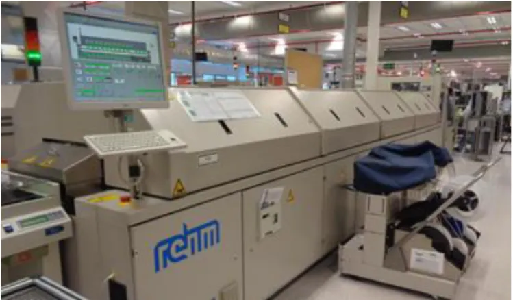
Figure 24. Bosch Car Multimedia Reflow oven, REHM, utilized to SolarA production. ... 35
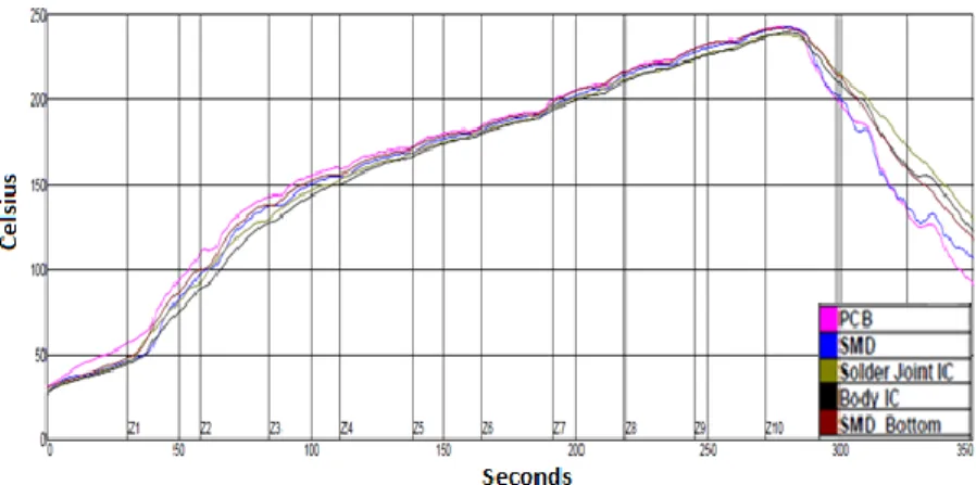
Figure 25. Temperatures registered by thermocouples placed in the standard plate, during the Reflow. ... 36
Figure 26. Bosch Car Multimedia Braga automatic inspection equipment’s: a) SPI; b) AOI of the Reflow soldering process. ... 39
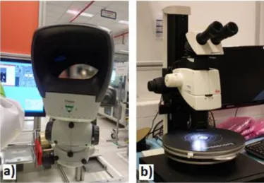
Figure 27. Bosch Car Multimedia Braga visual inspection equipment’s: a) Lynx dynascopic microscope; b) Leica M205C optical microscope... 40
Figure 28. a) X-ray image of part of the SolarA product (after Reflow process); b) Bosch Car Multimedia X-ray scanner inspection equipment. ... 41
Figure 29. a) University of Minho TGA-DTA equipment, SDT 2960 from TA Instruments; b) DTA-TGA process scheme [adapted from [63]]. ... 42
Figure 30. Bosch Car Multimedia optical microscopy, Keyence VHX-2000. ... 43
Figure 31. a) Mounted samples from university and b) Mecapol 260, used at University of Minho in (Inventor drawing). ... 44
Figure 32. a) Mounted samples from SolarA product cuts and b) Polishing machine Struers RotoPol-21 [adapted from [66], used at Marques Ferreira chemical lab. ... 45
Figure 33. a) Areas of sectional cuts: 1- resistor and capacitor; 2- QFP; b) Samples resulting from the cuts. ... 45
Figure 34. Bosch Car Multimedia scanning electron microscopy (SEM) and Energy dispersive X-ray spectroscopy (EDS), Hitachi TM3030Plus. ... 46
Figure 35. Results from the solder paste printing of all PCBs – QFP component. ... 48
Figure 36. Average of errors detected by the AOI per PCB: a) SolarA normal PCBs; b) SolarA PCBs with “2wt% Ni flux”. ... 50
Figure 37. Images obtained by visual inspection of three PCA components (chosen randomly) soldered in N2 and in Air atmospheres. ... 51
Figure 38. Images obtained of the X-ray inspection to the SOT component soldered in Nitrogen (a) and in Air (b) atmospheres. ... 52
Figure 39. Average of percentage area of voids detected in the X-ray inspection, for the 10 PCBs analyzed, soldered in different atmospheres. ... 53 Figure 40. Optical microscope images obtained from the cuts made on a QFP (a) a Capacitor (b) (left) and a Resistor (right) (c). ... 54 Figure 41. SEM example images of the local where the heights was measured from the: QFP soldered in Nitrogen (a) and in Air (b); QFP soldered on the PCB with “2wt% Ni flux” soldered in Nitrogen (c) and in Air (d). ... 54 Figure 42. Optical microscope images of the solder joint geometry from the components soldered on normal board: soldered in Nitrogen, QFP (a), Capacitor (c) and Resistor (e); and soldered in Air QFP (b), Capacitor (d) and Resistor (f). ... 56 Figure 43. Optical microscope images of the solder joint geometry of the QFP component soldered in N2 (a) and in Air (b). ... 57 Figure 44. IPC-A-610D acceptance criteria of Class 3 for the SMD solder fillet [adapted from [53]]. ... 57 Figure 45. Images of the solder joint formed at the QFP left pin, soldered on a normal PCB in a Nitrogen atmosphere (a) and corresponding elemental maps Sn (b), Cu (c), Ni (e), Ag (f), and all maps combined (f), in a scale of 100 μm. ... 58 Figure 46. SEM-EDS elemental mapping of the QFP, Capacitor and Resistor left pin (lead), soldered on the board with “2wt% Ni flux” in a Nitrogen atmosphere (scale of 30 μm). ... 59 Figure 47. Results obtained from the reactions of Nickel in the solder during the Reflow soldering: a) example of the results obtained in this dissertation; b) results obtained from a scientific paper [adapted from [38]]. ... 60 Figure 48. Optical microscope images of some examples of the intermetallic layer after Reflowing in N2 and in Air atmospheres. ... 61
Figure 49. Intermetallic thickness average values measured in different atmospheres to the: a) IMC pad-solder b) IMC solder-component; c) IMC pad-solder (PCBs with Ni); d) IMC solder-component (PCBs with Ni). ... 62 Figure 50. SEM images resulting from the pulverization of the “2wt% Ni Flux” on the substrate surface, representing the distribution in different scales a) 2 mm, b) 50 μm and c) 20 μm. ... 63 Figure 51. Histogram of Ni particles size distribution obtained from 30 measurements made to the particles pulverized on the substrate surface. ... 64
Figure 52. a) Represents the average diameter from the Ni particles added on the PCBs surfaces measured after the Reflow soldering process in N2 and in Air atmosphere. b) Represents an
example a Ni particle found in a sectional cut analyzed. ... 65 Figure 53. Normal substrates soldered at 260ºC (a) and (b), and substrates soldered with “2wt% Ni flux” added (c) and (d), at different atmospheres, in Argon and in Air (without Ar). ... 67 Figure 54. SEM images of some substrates with Ni particles soldered with SAC405 in different temperatures and atmospheres, in Argon and in Air (without Ar). ... 68 Figure 55. Average diameter from the Ni particles added on the substrates surface, soldered with SAC405 in Argon and in Air atmospheres. ... 69 Figure 56. Thickness average values of the intermetallic layers measured from the SAC405 samples soldered at different atmospheres: a) normal substrates; b) substrates with “2wt% Ni flux” added... 70 Figure 57. SEM image examples of the resulting intermetallic layer of soldering SAC405 on normal substrates soldered (a) and on substrates with Ni particles added (b), in the same conditions. . 71 Figure 58. Substrates soldered at 250ºC: normal substrates (a) and (b); substrates soldered with Ni particles added (c) and (d), at different atmospheres, in Argon and in Air (without Ar). ... 72 Figure 59. SEM images of some substrates with Ni particles soldered with SAC305 in different temperatures and atmospheres, in Argon and in Air (without Ar). ... 73 Figure 60. Average diameter from the Ni particles added on the substrates surface, soldered with SAC305 in Argon and in Air atmospheres. ... 74 Figure 61. Thickness average values of the intermetallic layers measured from the SAC305 samples soldered at different atmospheres: a) normal substrates; b) substrates with “2wt% Ni flux” added... 75 Figure 62. SEM image examples of the resulting intermetallic layer of soldering SAC305 on normal substrates soldered (a) and on substrates with Ni particles added (b), in the same conditions. . 76
L
IST OFT
ABLESTable 1. Variables that effect oxidation in Reflow soldering process [adapted from [43]]. ... 22
Table 2. Solders used at the university to this project. ... 33
Table 3. Elements used at the university to this project. ... 33
Table 4. Temperatures and velocity set in the Reflow oven... 35
Table 5. Conditions used in TGA-DTA to the soldering tests used in the study of adding Ni into the liquid flux. ... 37
Table 6. Number of PCBs analyzed and the total of errors and pseudo-errors detected, for each condition. ... 49
Table 7. Average values of the heights of the left pin of the QFPs measured. ... 55
Table 8. Average diameter measured from the Ni particles pulverized on the substrate surface (30 measurements). ... 64
Table 9. Melting temperatures of the SAC405 and SAC305 tested in an inert and oxidant atmosphere at heating rates of 5, 10 and 30ºC per minute. ... 66
L
IST OFA
BBREVIATIONSAg Silver Ar Argon
AOI Automatic Optical Inspection Cu Copper
DSC Differential Scanning Calorimetry DTA Differential Thermal Analysis
EDS Energy Dispersive X-Ray Spectroscopy ENIG Electroless Nickel - Immersion Gold FR-4 Flame Resistant 4
HASL Hot Air Solder Levelling IMC Intermetallic compound IPC Institute for Printed Circuit N2 Nitrogen
Ni Nickel O2 Oxygen
OSP Organic Surface Preservative Pb Lead
PCB Printed Circuit Board PTFE Polytetrafluoroethylene QFP Quad Flat Pack
RoHS Restriction of Certain Hazardous Substances SAC Sn-Ag-Cu
SEM Scanning Electron Microscopy SMD Surface Mount Device SMT Surface Mount Technology SOT Small Outline Transistor Sn Tin
SPI Solder Paste Inspection TGA Thermogravimetric Analysis TH Through Hole
THT Through Hole Technology
C
HAPTER
1
:
I
NTRODUCTION
Electronical devices such Printed Circuit Board (PCB), have been a subject of a huge investment by the industry, due to its efficiency and applicability. It can be used in numerous applications like, microwave and washing machines that require simpler PCB, and products such as auto-radios and computers which require more complex devices.
Printed Circuit Board is the most common method to support and electrically connect electronic devices such resistances, capacitors, among other, creating the electronic circuits. For that is utilized a substrate (board) which is an electric insulating material, where are printed the conductor tracks and pads, that allow the electrical connection of the components to each other. These substrates can be formed by one or more Copper printed layers according to the complexity of the electric circuit, which is growing rapidly due to the high requirements of new electronic devices require [1].
With the development of more complex products, the PCBs requirements have increased due to the increasing of the packing density of the components. This results in: diminishing of the space dimension between the components; the holes diameters are decreasing; the conductor tracks are thinner; and the PCB boards have more layers. With this, the integrated circuits have become more complex (e.g. implementation of microvias), PCBs design has to be planned carefully and components assembly is more difficult [1].
The connection board-component is made from a soldering process creating a solder joint between them that is responsible for the mechanical and electrical connection. The soldering processes most used industrially are Reflow and Wave soldering. With these soldering processes it is possible to make mechanical and electrical connection between the components and the boards with a solder joint. The quality of the solder joints depends essentially of the type of solder, thermal cycle and the atmosphere used [2].
The solder joints need to be constantly studied with the development of PCBs, because the increase of components density and less space on the board results in a higher probability of defects to occurrence. This way, the thermal cycle must be planned so that the PCBs are subject
to a specific temperature in a given period of time, in order to obtain an adequate intermetallic between the components, solder and pads [2].
Other parameter that influence the solder joint and the presence of soldering defects, is the atmosphere used. Normally the soldering processes use an inert atmosphere like Nitrogen (N2), in
order to reduce solder defects like oxidation, which may cause a bad solder joints. But the use of a high flow inert gas, normally involves high expenses [3].
This way, in partnership with Bosch Car Multimedia from Braga, was developed the project of "Reflow Soldering in an Oxidant Atmosphere". This dissertation is intended to: evaluate the influence of soldering in an oxidant atmosphere (Air atmosphere) on joint quality; evaluate the influence of soldering in an inert and oxidant atmosphere and with adding Nickel into the liquid flux. These studies are intended to evaluate the solder microstructure, intermetallic layer thicknesses and solder joints geometry, to quantify the defects, wetting and spreading.
1.1 Motivation
The soldering processes as Reflow soldering, allows to create an electrical and mechanical connection between the components and PCB boards, creating the solder joints. The characteristics of solder joints depend essentially of the type of solder, thermal cycle and the atmosphere used. These process parameters may influence the solderability of the solder, solder joints geometry, thickness of the intermetallic, wetting and spreading, this way, defects can appear.
To create these solder connections, the electronic industry traditionally used lead solders, namely the Sn-Pb (Sn63Pb37) solders, due to its high solderability and low melting point (183ºC), comparably to other solders. But from 2006, the lead solders began to be forbidden due to their toxicity to the environment and human being according to European Union’s Restriction of Hazardous Substances (RoHS) Directive and Waste Electrical and Electronic Equipment (WEEE) Directive. Then, to substitute the Lead solders, began to emerge the first lead-free solders (solders without Pb in their composition) in industry [4, 5].
The use of the Lead-free solders, according to their specification, soldering need higher temperatures (about 217ºC) comparing to the temperatures used with Pb solders (about 183ºC). This way, the increase of the soldering temperatures can cause problems such as higher susceptibility to oxidation and increasing of the energy expenditures. In other to avoid the oxidation problems, industries utilize a neutral atmosphere (e.g. N2), but with this, the soldering processes
Since Nitrogen is an expensive element, it is intended, when possible, to eliminate it. This way, in partnership with Bosch Car Multimedia from Braga, was developed the project of "Reflow Soldering in an Oxidant Atmosphere". At this dissertation is intended to the study of alternatives to reduce solder oxidation, in order to eliminate or reduce N2 spending. These alternatives undergo
by testing the soldering process in an Air atmosphere, and the addition of an alloying element in the soldering process.
1.2 Objectives
This project has the main objective, the study of alternatives to reduce solder oxidation, in order to eliminate or reduce N2 spending.
Specific Objectives:
Evaluate the influence of soldering in an oxidant atmosphere (Air atmosphere) in the solder joints geometry, presence of possible soldering defects, and in the intermetallic thickness;
Evaluate the influence of soldering in an inert and Air atmosphere, with adding Nickel micro particles into the liquid flux.
1.3 Dissertation Structure
This dissertation is divided into five chapters.
In chapter 1 is presented a brief overview of this thesis work where are presented the motivation and the objectives to be achieved.
In chapter 2 is approached the review of the literature with the concepts related to the project theme. First are presented the concepts related to the Printed Circuits Boards and components. Secondly are presented the concepts related to soldering, like the solders used, soldering processes and parameters, and finally are presented some of the soldering defects that exist.
In chapter 3 are presented the materials and experimental methods used in this project. It is presented: all the materials used in the project realized at Bosch Car Multimedia and at the University of Minho; the processing methods which are explained the procedures and parameters used at Reflow soldering process; the inspection and qualifying techniques used to qualify the products produced at the production; finally are presented the characterization techniques used.
In chapter 4 are presented and discussed all the results obtained from the characterization techniques. In this chapter as the previous, were divided the results obtained at Bosch and the
results obtained at University. First are presented the results obtained in the inspection and qualifying techniques, then are presented the results obtained in the characterization techniques for each condition used (soldering in N2 and Air, and with the addition of Nickel micro particles on
PCBs/substrates).
In chapter 5 are presented the conclusions obtained from this study, and the proposals of possible future works.
C
HAPTER
2
:
R
EVIEW OF THE
L
ITERATURE
In this chapter are presented the main concepts related to soldering in electronic industry. First are referenced the Print Circuit Boards in which are presented the principal types of PCBs and surface finishes used in the industry. Then are covered the components, in which are presented some type of components used in the electronic industry.
Secondly are presented the concepts related to soldering, where are: explained the type of solders normally used in the industry; explaining the soldering processes, mainly Reflow process; and the parameters normally utilized; and finally some of the soldering defects that exists are explained.
2.1 Printed Circuit Board (PCB)
Electronic devices resulting from a combination of electronic components connected one to another through a plate named Printed Circuit Board (PCB). PCBs are used in diverse electronic devices, in order to provide mechanical support to the components and electrical connection between them, forming the electrical circuits [6].
In 1936, Paul Eisler made a significant contribution in the electronic industry with the invention of PCBs, and in 1943 he patented this method of etching circuits on a copper layer bonded to a non-conductive base, reinforced with glass. Then the advance of electronic technology, the components became very small, and manufactures reduce the overall size of the PCB and the electronic package [6].
PCBs are constituted by one resistant and non-conductive substrate on which are printed the layers, conductor tracks, pads and vias. The substrates generally used are the FR-4 (glass fiber plus resin) and PTFE (commercially known as Teflon) by having a low electrical conductivity, acting as a barrier between the printed electrical conductor tracks [7].
Layers and printed tracks are made of a conductive material normally copper. A simple PCB normally has two copper layers, in the top and bottom of the PCB, but with the advance of technology, PCBs may have more than 2 layers. The electrical connection between these layers are made through a hole in the board, named vias or microvias that are also made of cooper too. Some vias are covered by solder mask to protect them from being soldered [1].
The connection between the electrical component and PCB are made through the pads that are a portion of exposed metal on the surface of a board to which a component is soldered. These pads are terminals made of copper that normally have a conductor surface finish to protect from oxidation, but without damaging the electrical connection. The electrical components can be attached to the PCB by to different technologies:
Surface Mounted Technology (SMT), where components are mounted, or directly placed, and soldered onto the surface of the PCB. This technology uses more compact components, and higher circuit densities can be used on smaller boards. This is especially important, because today, electronic industry are growing more complex and more compact [8];
Through-Hole Technology (THT), where the components lead wires are inserted into metallized plated holes that cross completely the PCB and soldered to the walls of the hole. This technology is extremely reliable, as it provides strong mechanical bonds, however, the holes makes the production of boards significantly more expensive. This kind of components are larger, which results in a lower density per area [8].
Finally, PCBs also have a solder mask film placed on the plate in order to isolate the copper tracks from contact with external agents, leaving only discovered the zones to solder, pads for example.
Figure 2. Schematic representation of a PCB.
2.1.1 Classification of PCBs
Printed Circuit Boards may be classified according to the specifications and requirements of the final product, such as automotive and non-automotive applications, but principally based on the number of layers, and type and number of components used. This way, PCBs may be:
Single-sided PCBs, which consists in a board where, all electrical components are fixed on one side but soldered in the other side (figure 3a). This PCBs are used in cases of simple circuits, so the manufacturing costs are low [1];
Double-sided PCBs, also named 2-layer board, is the most common type of board where electrical components are attached to both sides of the substrate (figure 3b). This kind of PCBs have only two layers connected to each other through plated through-holes. Comparing to the single-sided PCBs, these are more expensive because their higher complexity. This is the type of PCB studied in the dissertation (SolarA product) [1, 7];
Multi-layer PCBs, which are similar to the double-sided PCBs, but have more than two layers, because in some situations the necessity of having more density connection, is high to be handled by only two layers (figure 3c). The manufacturing costs depends upon the complexity of this type of PCBs (more complexity, more costs) [1, 7];
Flexible and Rigid-Flex PCBs, which are classified on the basis of the type of material used in the board, flexible material (figure 3d). These flexible boards are very thin (range of 0,1 mm thickness) with copper on both sides in rolls, and are used in application with restriction of space and low weight. The manufacturing costs depend upon the complexity of the PCB, and the materials used to his production [1, 7].
Base material (FR-4)
Copper Layers
Figure 3. Schematic representation of various types of PCBs. a) single-sided PCB; b) double-sided PCB; c) multilayer PCB [Adapted from [1]] and d) rigid-flex PCB [Adapted from [9]].
2.1.2 PCB Surface Finishes
A surface finish, in a simple explanation, is a protective coating film applied on the surfaces of the PCB, to protect the exposed copper (pads and plated through holes) to preserve solderability and reduce possible defects that occurs after soldering (figure 4). Independent of the coating materials used, they need to guarantee: a good solderability during the soldering process in other to have a reliability solder joint; protect the exposed cooper from oxidation and deterioration until the component assembly, and finally minimize the copper dissolution during the soldering process [10, 11].
Every finish material has their own benefits, but the process, product or environment will dictate the surface finish that is best suited for the application. So, it is important that the PCB designer or assembler work, close with the PCB supplier in order to select the best finish for the specific product. The appearance of the new solders alloys (lead-free) affects the compatibility of the finishes with the metallurgy of the solder joint. This may influence the pad wettability, the plated through holes fill, appearance of voids and others defects that may put in question the reliability of the final product [10, 11].
In the industry many types of surface finishes are used, but the most used and mentioned in the literature, are:
Hot Air Solder Leveling (HASL/Lead-Free HASL): consists in a solder alloy coating (figure 4a) to protect the copper exposed on the PCBs. At the beginning this coated film is composed by a Lead solder (Sn63Pb37) and most surface finish mostly used because the high solderability. This happens because the solder and HASL have the same chemical composition, then “Nothing
solders like solder”. With the legislation and appearance of the lead-free solders, the soldering process parameters was changed, as the process temperatures [10, 11].
To create the HASL finish, the PCB is bathed in a molten solder that covers all the copper surfaces exposed, then with hot Air knives, the excess solder are removed from the surface. HASL provides a very reliable solder joint, making the component soldering very effective, cheaper and of easily application, and have a long shelf life. But, due to the irregular thickness of the coating this film has poor coplanarity, which can be unsuitable for fine-pitch components [11, 12].
Organic Solderability Preservative (OSP): consists in an organic coating (figure 4b) to protect the copper exposed on the PCBs from the environment until and during the soldering processes, when the PCB suffer more than one soldering process. When this happens, the OSP coating needs to resist the thermal degradation that the soldering process (e.g. Reflow) imposes. For that, this coated film need to have a sufficient thickness to resist this conditions, so the thickness are around 0.2 and 0.5 μm. During the soldering process, the solder temperature or solder flux, can remove /degrade the OSP film allowing the soldering [10, 11].
This surface finish is cheaper and of easily application, but, it is easily degraded by temperatures, and it has a difficult inspection and a limited shelf life [11, 12].
Electroless Nickel/ Immersion Gold (ENIG): consists in a double layer metallic coating (figure 4c), Nickel and Gold, where nickel acts as both a barrier to the copper and a surface which the components are soldered. The Gold layer protects the Nickel during the storage. It is the most popular surface finish in the industry because it answer to major trends such as lead-free requirements and the rise of complex components which require flat surfaces. To prevent the mixing of Au with Cu, and the eventual solderability problems caused by oxidized copper at the PCB surface, layer of nickel is deposited to separate them. ENIG has a thickness about 3 to 6 μm of Ni, deposited by electroless Nickel plating, and 0.05 to 0.125 μm of Au obtained by immersion Gold plating [10, 11].
ENIG has excellent solderability, long shelf time, works well with lead-free solders and has a high consistent thickness. On the other hand, this coating is expensive, cannot be reworked and can cause “Black Pad Issues”, which consist in a buildup of phosphorous between the Ni and Au layers that can result in faulty connections [11, 12].
Imersion Tin: consists in a thin coating of pure Tin (figure 4d), with a typically thickness about 0.6 to 1.2 μm, which protects the underlying cooper from oxidation and provides highly
solderable surface. This surface finish is produced by immersing the board in a Tin bath (galvanic displacement process), forming an intermetallic with copper that could be a challenge to shelf life [11, 12].
Immersion Tin has a low manufacture cost, a flat surface, good solderability and can be reworked. On the other hand, the thickness is difficult to measure, it can produce a brittle intermetallic, and degrade with time and multiples Reflow soldering, and can occurs solder mask attack (during this coating manufacturing) [11, 12].
Figure 4. Examples of the most used PCB surface finishes: a) HASL; b) OSP; c) ENIG; d) Imm. Tin [13].
2.2 Components
Electronic components are assembled on the PCB to complete the electric circuit and form a functional and operating system. These components are incorporated in the electric circuit by soldering them to the pads of PCBs, where solder makes an electrical and mechanical connection [14].
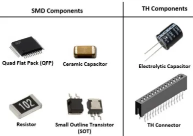
Today in the market it is possible to find a great variety of electronic component packages, according to the manufacturing requirements and performance needed for the final product. Then, there are two types of components, Surface Mounted Devices (SMD) and Through Holes (TH) (figure 5). In a simple explanation, SMD are all those components that are soldered in the same side of the PCB, where the component are placed. TH are all those components that have pins (lead wires) intended to be mounted through a plated hole, and are soldered to the opposite side of the board from which the component was inserted (normally mounted in just one side of the PCB [8, 15].
Actually, in the electronic industry the tendency is to replace most TH components by the SMD because the development of the technology and the emergence of complex and small electronic products. This way, comparing SMD with TH devices, these are:
Smaller than TH type, allowing the design of smaller and denser PCBs, and enable applications that would be impossible with TH components;
A type of components which can be mounted on both sides of the PCB (if necessary), and their placement and processing lends themselves to fully automated assembly, reducing assembling costs [8, 15];
On the other hand, SMD have some disadvantages when compared with TH, which are:
High investments on machinery because of the need of an automatic production;
Some large components like the higher-power components, can’t be SMD type;
Soldering processes with higher parameters and restrictions, which may lead to occurrence of more defects. It’s harder to test and rework SMD boards comparing with TH [8, 15]. In figure 6 are presented some examples of SMD and TH components mostly used in the industry, and at Bosch Car Multimedia product (SolarA) used.
Figure 6. Examples of SMD and TH components used in SolarA product.
2.2.1 Components Metallization
The electrical components have to be attached to the PCB during soldering, so, for this, the components lead material must be electrically conductive, and have affinity with the solder. The most common material used in components leads is copper, and as it is known, this material is
susceptible to oxidize by the environment, time and principally by the number of thermal cycles which the components are subjected. So, to protect and minimize these effect of the components leads (pins) some kind of protection is needed to be apply, in other to assure solderability during soldering.
Like PCBs, the solution to this problem is to apply a barrier that protect the surface to solder by applying a protective layer to the components leads (metallization) [14].
Figure 7. Scheme example of the electric components metallization.
In the electronics industry, as in the case of Bosch, the majority of the components have a copper base material (about 80% of all products), but according to the type of component or the specifications of some products, other base material (e.g. FeNi) can be used. To protect this base material, the most used finish layer utilized is Sn, and according to the final product application, this layer can be applied with different thicknesses. Lastly, there are components, which according to some requirements and to avoid some defects, need to have an intermediate layer of Ni or Cu (between Cu-based and Sn layers) [16].
2.3 Introduction to Electronic Soldering
Soldering is a technology that has been used for thousands of years, as in the Roman times where they made solder connections of the aqueducts pipes with a mixture called tertiatium [17]. Actually, soldering has been used in many applications, but with the emergence of electrical technology, it takes an important role in the electronic industry [18].
This way, soldering is a technique used to join two materials together using a filler (the materials normally used are metals). The connection of these metals are made by a filler molten alloys with melting temperatures below 450ºC, where this alloys are a mixture of two or more pure metals with lower melting point than the metals to solder. The molten solder need to be capable of wetting the metals to solder, forming an interphase (intermetallic) near to the joint where the
microstructure is altered, and solidifying creating a conductive and resistant bond between them [17, 18].
To the Printed Circuit Boards soldering, is using low-temperatures filler metal, which is usually a tin-containing alloy. In order to have the wettability obtained at a temperature of 450ºC, but using low-temperatures (about 183ºC to 220ºC), a fluxing agent is used, also called flux. This flux assist the wetting on the basis metal by dissolving the oxide film present and clean the interface to solder [18].
So, during the soldering process the molten filler metal reacts with a small amount of the base material (normally copper pad) and the component lead, forming an intermetallic compound. After soldered, the component is expected to be attached to the PCB, through a solder joint that connects the component leads to the PCB pad. At figure 8 is shown a schematic of what is obtained after a soldering process [17].
Figure 8. Constitution of a solder joint (SMD component – lead of a QFP).
A few years ago, the soldering processes utilized eutectic or near eutectic solder alloys of Tin and Lead (63wt%Sn – 37wt%Pb), which begin to melt at 183ºC. But now, due to the legislation that forbids the use of Pb solders, appear the free solders (solders without Pb). These Lead-free solders requires higher process temperatures, so, may be necessary to change the components, PCB boards and even process equipment’s. This way, it should be taken into account the process parameters and control the process window [19].
2.3.1 Soldering Basics
In soldering it is necessary to take into account some concepts to obtain the best solder joint possible, which depends strongly on the combination of filler and component materials (surface coatings), and also the process conditions used.
To occur soldering it is necessary that the solder has to be in contact with materials to solder, like component and pads of the PCB. The spreading of the solder on the surfaces to solder, is influenced by wetting and surface tension effect, and it must have good solderability in other to form an interphase, intermetallic, resulting of the chemical reaction of the solder with the surface to solder. [19].
Wettability is defined as the tendency of a fluid to adhere or spread over a solid surface, establishing a contact angle which results from the balance between adhesive and cohesive forces. The liquid phase will spread over the solid surface until the three surface tensions: between the liquid and the solid surface (𝛾𝑆𝐿); between the liquid and the atmosphere (𝛾𝐿𝑉); and between the solid surface and the atmosphere (𝛾𝑆𝑉), are in balance, according to equation 1.
𝛾𝑆𝐿 = 𝛾𝑆𝑉 − 𝛾𝐿𝑉. 𝑐𝑜𝑠𝜃 (Eq.1)
According to this equation, the contact angle θ provides a measure of the quality of wetting, in other words, if 90º < θ < 180º, some wetting occurs but the liquid won’t spread on the surface. So, the smaller the contact angle, θ < 90º, better will be the wetting and spreading over the area to solder (figure 9) [20].
Figure 9. a) Surface tension forces according to the classic model of wetting; b) effect of the contact angle on fillet formation and geometry [adapted from [20]].
Wettability and spreading can be affected by parameters such as temperature, time and metallurgical and chemical nature of the surfaces. High temperatures increase the atomic activity, the reaction rates and the fluidity of the liquid solder, which results in a better wetting. In the other hand, higher promotes the formation of oxides. Time is important, because it is necessary to have
necessary heat conditions, to flux action, to initiate wetting and time to spreading occurs. The nature of the surfaces affects wetting and spreading, because some surfaces are easily wet than others. The presence of oxides, oil and silicone or other type or residues need to be cleaned to not interfere with wetting. The coating films to protect from oxidation, like OSP can be a problem to this phenomena too [17].
Solderability is defined as the ability of a metal to be wetted by a molten solder, and it depends on the wettability of the two surfaces to be joined. This phenomenon is important to have a reliable solder joint, to use less active fluxes (less aggressive), and finally to obtain a greater solder fillet geometry and resistant to mechanical stresses [17].
During the storage and soldering process, solder surfaces can oxidize especially in an Air atmosphere, so this is a problem that reduce solderability. This way, it is necessary to find a solution to reduce or eliminate this problem. Then, the solution found to this oxidation problem is the application of a chemical agent, flux, during the soldering process [19].
Soldering Flux is a liquid or solid material which, when heated are capable to promote wetting by removing tarnish and oxidation [19]. It also acts as a barrier preventing from re-oxidizing of the melted solder, and has to ensure that it flows over the surfaces to be bonded without interference of the oxide layer that may form during the process (figure 10). Fluxes need also to be harmless to components to solder, be easily removed and thermal stable at the process temperatures [21, 22]. But due to the flux be in the solder paste or be directly applied to the surface of the PCB, the oxidation problems may be more problematic in the components pins (leads). This can happen because the flow cannot act in full on the surface of the solder pins.
Figure 10. Schematic of the function of the flux in soldering [adapted from [22]].
Several types of fluxes are available in the industry, but only two broad categories are most used. One is the clean flux, also known as water-clean flux, which is composed of relatively strong organic acids and may be fortified with halogens to increase its chemical activity. This type of flux need to be washed from the surface printed circuit assembly after soldering, to avoid corrosion
and electrical failure. The other type of flux is rosin-based, with additives to change the characteristics of the flux, increasing is activity and aggressiveness. To remove this type of flux from the printed circuit assembly some solvents are necessary, but as the resulting residues are inert, they can remain on the board surface, called the no-clean fluxes [21, 22].
Even if guaranteed the process ideal conditions, and absence of possible factors which influence the solderability, it must be ensured that, exists the formation of an interphase between the solder and the surfaces to solder (PCB and components), named intermetallic compound (IMC).
Intermetallic is a layer created at the boundary of the liquid solder and the solid surfaces (diffusion zone). The intermetallic is the key to soldering, because without IMC, there is no solder joint. So, for this layer to be formed, the metal surfaces need to be metallurgically compatible with the solder to create the interphase which holds them together (figure 11). The volume of the intermetallic compounds formation, depends essentially on temperatures and time during the process, and during its formation, the base metal dissolves in the molten solder in a quantity that depends on its solubility in the solder [17, 19].
Intermetallic compounds are more like a chemical compounds than metallic alloys, and they act like a glue that forms the structural bond between the solder and the surface metals to solder. But this layer can cause several problems because:
It is a brittle material that decreases the mechanical reliability (liable to crack);
They generally have poor electrical conductivity comparing to solder and base materials [17, 19].
Figure 11. Schematic cross-section of a SAC solder joint – Intermetallic compound [adapted from [22]].
For Bosch, as the goal is to reduce the maximum production costs (e.g. the energy), the process window is set to form the as soon as possible between the intermetallic between the pad-solder and pad-solder-component, no matter their thickness.
2.4 Solders
Solders are metals or metallic alloys normally used to join metallic surfaces as in the case of electronic industry. To form a solder joint, these metals alloys have to be melted and have a melting point below that the metallic surfaces to join [23]. These solders can be provided in two ways, in wire or solder paste, according to the type of soldering process used. Manual and Wave soldering normally use solder in wire form. In the case of Reflow soldering is utilized solder pastes, which consist in small solder particles with dimensions in the range of 5 – 75 μm [24], mixed in liquid flux.
Solders used for electronics are normally made by a combination of Tin and other elements in different proportions, and is possible to find various types of solders available in market. Solders aren't made only by Tin, because the cost comparing to other materials is higher, and higher Tin contents in solders can have limited applications and less proprieties [25].
During the years, electronical industries used the Sn-Pb (Sn63Pb37) solder, due to its high solderability and low melting point (183ºC), comparably to other solders. These solder is a eutectic solder, because according to the Sn-Pb phase diagram, to this two elements ratio, the solder changes from liquid to solid directly at 183ºC, without an intermediate phase (plastic phase) [26]. But from 2006, the solders with lead began to be forbidden due to environmental concerns (toxicity to the environment and human being) according to European Union’s Restriction of Hazardous Substances (RoHS) Directive and Waste Electrical and Electronic Equipment (WEEE) Directive. Then, to substitute the Lead solders, began to emerge the first lead-free solders (solders without Pb in their composition) in industry [4, 5].
Lead-Free solders have similar properties as lead solders, but presents differences like higher melting point and surface tension and do not wet or spread so good as the Pb-solders. In practice the main problem of the lead-free solders is that their melting temperatures are not as low as Lead solders. Pb solders melts at 183ºC and Lead-Free solders melts in the range of 217 to 229ºC, according to ratio and composition of each solder [5, 26].
2.4.1 Types of Solder
With the development of electronic industry, the requirements are higher, so it’s necessary to find new solutions to respond to these necessities. With the reduction size of the electronical devices, the components packaging and density on the PCB makes that the available areas to solder are increasingly small. This way, the probability to occur defects, combined with the existing
problems of oxidation during the process, requires the existence of specified solders for each application [1].
Since the Lead solders left the market, many types of Lead-Free solders starts to appear in the industry, as it is possible to see in figure 12. So according to each soldering requirements, there are solders with different compositions and ratios capable to soldering in Air atmosphere, with lowest temperatures, no-clean solders, among others specifications.
Figure 12. Principals Lead-Free solders used in Reflow process - European Lead-Free Soldering Network, released
March 2007 [adapted from [27]].
According to IPC norms, the family of Tin-Silver-Copper alloys, denominated SACs, are the solders recommended in the electronic industry, as the replacement for the lead solders. Since Pb solders were forbidden, SAC solders became the industry standard. The SAC most used are SAC305 (96.5Sn – 3.0Ag – 0.5Cu) and SAC405 (95.5Sn – 4Ag – 0.5Cu), which, according to the Sn-Ag-Cu phase diagram, are near to the eutectic point, characteristic of a melting point about of 217ºC (figure 13). From all the existent Lead-Free solders, these two are the ones with the closest properties to the Pb solders [25, 26].
Figure 13. Section of the ternary phase diagram corresponding to SAC solders compositions mainly used in soldering (marked in red) [adapted from [28]].
It’s very important to consider the microstructure during the fabrication, because small changes in the composition can lead to a large differences in microstructure. In order to avoid this problems and possible defects during the soldering process, the solidification behavior needs to be studied [25, 26]. But these solder alloys have also the advantage of modify their composition, by adding other elements, in order to improve their properties. Then, this is possible by adding alloying elements, like Zinc, Aluminum, and Bismuth for example, to study their effects on SAC alloys [26].
2.5 Solder Alloying Elements
Since Pb-solders, solders with identical properties have been used, Lead-Free solders. However, many problems of these solder alloys (especially SAC) still exist, such as the higher melting temperatures, less wetting than Lead solders, large brittle intermetallic and high costs [29]. This way, with the development of soldering industry technologies such SMT fine-pitch design (the fine spacing between the pin leads, spacings of 0,65 mm or less [30]), as well as the increasing environment requirements, is necessary to investigate and create new Lead-Free solders with better proprieties [29]. In order to enhance the properties of Lead-Free solder alloys, elements such as Bismuth (Bi), Indium (In), Gallium (Ga), Zinc (Zn), Nickel (Ni) among others, can be selected to be added into these alloys [25, 26, 29].
There are many methods to intervene in the solder to obtain the final properties expected, such as better wetting, spreading, lower melting temperatures and finally the mechanical strenght of for the solder joint. One of them consists by adding micro or nanoparticles, which does not involve a diffusion process and the production of a new alloy, but participation in the solder system [29, 31].
For this, in this dissertation will be studied the effect of adding micro particles of Ni into the flux, which will be placed before the soldering process.
Nickel:
In literature, it is possible to find that Ni has already been subject of study as an alloying element in some solders, and also studied the influence of adding in micro or nanoparticles in the solder. This way, it is possible to know the properties of a Lead-free solder when adding Ni.
According to some research made, it was seen that when adding Ni in the alloy form into Lead-Free solders, it:
Influence the morphology and thickness of IMCs, when added in the form of nanoparticles or as an alloying element addition [32];
Improve mechanical properties, and provide a diffusion barrier between Cu and Sn based solder alloy, in order to prevent, or at least suppress the formation of the Cu3Sn phase [33];
Decrease the wetting force [33], increase the wetting angle [32, 34, 35] and have longer wetting time [34].
When it comes to adding Nickel shaped particles, micro or nanoparticles, the effects on the final properties are slightly different. According to the literature, when the nanoparticles are added within the solder flux, the diffusion process is different with the presence of nanoparticles of Nickel, so they block the formation of voids. The Nickel particles are also capable to increase the shear strength of the Lead-Free solders [36].
When the Nickel particles are added into the solder paste, during the soldering process (e.g. Reflow), the intermetallic grow between the copper layer and solder, but also around the Ni particles in the form of “sunflower” (figure 14), named the sunflower shaped intermetallic particles [37, 38, 39]. This type of solder paste with particles of nickel, seems to produce no major changes in terms of wettability, comparing to the existent Lead-Free solders [40].
Figure 14. Effect of Reflow on the growth of intermetallic layers (sunflower): a) around the Ni particles b) at Cu substrate/solder interface with Ni, [adapted from [38]].
However, for this dissertation, the purpose of adding Ni micro particles is to evaluate their influence at the soldering process, in an inert and oxidant atmosphere, and expect to achieve better results.
2.6 Soldering Atmosphere
With the increasing of density and high performance of electronic devices, components are increasingly smaller, taking to a reduction in solder joint dimensions. As already mentioned, the solder joint has the function to conduct electricity and create a mechanical joint. This way, during the soldering process, it must ensure that there will be a good wetting and spreading, without presence of other defects that may call into question the solder joint reliability [3, 41].
2.6.1 Air Atmosphere
The main problem which can promote a bad soldering is the creation of oxides (non-solderable surfaces) in the zones to be soldered. This happens principally because the natural heat of the soldering process combined with the oxygen present on Air (about 210 000 ppm O2), oxidize
solder and the surfaces to solder, pads of PCBs and the pins/leads of the components [42]. One the other hand, during the soldering process, beyond the temperature and the oxygen concentration, oxidation is effected by the surface area, flux content and metal type/content [43].
Oxidation is directly related to:
Higher temperatures, because higher temperatures means faster rates of oxidation. Thus, to reduce the rate of oxidation it is needed to reflowing at the lowest possible temperatures [43];
Oxygen content and Air velocity, because the greater the concentration of oxygen in the Air, more likely to oxidize. With forced convection in the oven, the greater the amount of oxygen from particles which come into contact with the solder, increasing the oxidation [43];
Surface area, because with more exposed area, means more area available to oxidize. This refers to the pads/leads to be welded and the solder particles in the paste, because the smaller they are, it has more are exposed. This situation happens more often with the use of fine-pitch technology, because leads became finer and finer [43];
Metal content, because some metals are more solderable and propitious to oxidize than others. This way, surface metals need to have a coating to protect from oxidation, during the storage and all the soldering processes applied [43];
Flux activity, because to remove oxides is necessary aggressive fluxes, more activity. The no-clean fluxes contains a smaller amount of activators to reduce residues that remains on the PCB, however, with this reduced flux activity the oxidation may be a concern [43]. The
residues resulting from the reaction of the flux with oxides, have a brown or yellow coloration, which may disturb the inspection of solder joints [42].
Table 1 shows the variables, mentioned above, that effect oxidation. Table 1. Variables that effect oxidation in Reflow soldering process [adapted from [43]].
Oxidation variable Variable trend Reflow result
Temperature Higher Worse
Air velocity Higher Worse
Oxygen Content Lower Better
Exposed Area More Worse
Metal content Non-Tinned Worse
Flux activity Lower Worse
To avoid this oxidation problems, the solution may be to use an inert gas for the local atmosphere [42].
2.6.2 Nitrogen Atmosphere
Nitrogen (N2) is an inert gas very used in industry due to its properties and to be unreactive
at standard temperature and pressure. It is used in electronic applications, such automotive industry due to high quality and reliability that this gas can promote in solder joints. It is the most used inert gas because it is the cheapest available gas, about 78% of the Air composition, which does not react with metals, preventing their oxidation [3, 44].
Nitrogen atmosphere used during the Reflow process is known to improve the soderability by preventing oxidation of the surfaces to solder, improving the wetting and the reliability and quality of solder joints. Comparing to an oxidant atmosphere such as Air, Nitrogen can widen the process window of reflow soldering, reducing effectively the number of defects that possible can occur [44, 45]. The using of Nitrogen allows the utilization of No-clean fluxes, because the residues production are very low making the inspection of solder joints on finished PCBs easier [42].
However, Nitrogen have some negative points that must be considered like the high costs and tombstoning. This last defect, happens when using too much Nitrogen during the Reflow, so, having only a Nitrogen atmosphere, may bring defects [42]. This happens because, as PCB advances in the oven the part that goes ahead heats first, and so do the components. This way, the solder wet around the one and, the surface tension of the molten solder on that wetted end
results on the lift of the component before the solder paste goes molten and wets the other end. So this defects is most often seen on the smallest devices, as SMD Chip Capacitor and Resistors [42].
Then, to reduce this and some other defects, the atmosphere must be controlled and maintained an acceptable oxygen concentration to obtain a desired or best soldering performance. With some oxygen levels during the Reflow, the surface tension of the molten solder may decrease and the component do not lift. For this, and according to literature, the concentration level of oxygen may be about 1000 to 1500 ppm O2, to minimize tombstoning and obtain the best solder joint
possible [3, 42].
Finally, even with the advantages of using Nitrogen, due to its high price, it is always questioned whether the use of Nitrogen as the atmosphere in the soldering process is profitable. For this, all companies must evaluate the yield and costs associated with using this type of atmosphere [44],
2.7 Soldering Processes - Reflow
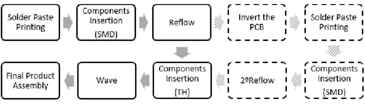
There are several methods for soldering, but with the advance of the electronic industry it is needed to produce in a large scale. This way, when a PCB is soldered a mass soldering techniques are required. The two most common for these high-volume manufacturing, are Reflow soldering and Wave soldering [2]. The soldering method is chosen by the types of components and PCB to solder, and the requisite solder joint proprieties. Sometimes, in accordance with the functionality and complexity of the products, it may be necessary to apply one or two reflows (the second only if necessary), and finally wave for solder the bigger and complex components [46].
In the industry for the production of an electronic product, the soldering process involves basically the following steps (figure 15):
As Reflow process is the main study in this dissertation, will be explained in detail ahead, here is a brief description of the Wave process which is not utilized.
Wave soldering is a large-scale soldering process which consists in using waves of molten solder to attach and solder components to the PCB. The process consists in first, inserting or placing the components into the PCB, than the loaded PCB passes across the top of a tank with molten solder with pumped waves. This way, the solder wets the exposed metallic areas of the board, those ones which are not protected with solder mask, creating an electrical and mechanical connecting [47].
Wave soldering is applicable to wired components (through-hole type) and SMD components too (minimum pitch 0.65 mm). However, these surface mount components need to be placed and glued to the PCB surface before being run through the molten solder wave [47].
The main stages of the reflow soldering process will now be described.
2.7.1 Solder Paste Printing
Solder Paste Printing is one of the first steps of the production, and it is very important because the reliability of the solder joint depends on it. In this step the PCB enters the printing equipment, the line stops and the solder parte is deposited at the points on the upper side of the PCB where the electrical and mechanical connection between the components and PCB are made. The deposition of solder paste onto the PCB contacts is achieved by applying pressure by passing a Squeegee over a stencil, then the solder passes through the stencil openings and it is printed on the pads. The stencil openings geometry must be accurate and match with the pads of the PCB. Each type of PCB have their own stencil [48, 49].
The solder paste is put on the stencil manually, and recharged by the line operator, and must be stirred for about 30 seconds in a homogeneous way, before placed on the stencil. So that the solder paste does not lose their properties, it should have a maximum of 8 hours of work on the stencil. The solder paste homogeneity, surface tension, Squeegee pressure, stencil thickness, alignment and distance between the stencil and PCB, temperature and humidity, are very important parameters to take into account to obtain a reliable solder joint [48, 49].
Figure 16 shows the solder paste printing equipment used at Bosch Car Multimedia Braga, and a surface printed PCB.
Figure 16. Bosch Car Multimedia: a) solder paste printing machine, EKRA; b) Stencil, solder paste and Squeegee; c) surface printed PCB.
2.7.2 Components insertion
The components insertion is the step that follows the solder paste printing, which consists in placing the components on which the solder paste was already placed. The components are placed on the surface of the PCB by means of automatic machines through a process called pick-and-place. The components are removed from the feeder through a nozzle, placing each component in the intended place of the PCB [48, 50].
The placement of the components should be as fast as possible (about 25000 components/hour) in order to avoid possible defects caused by long exposure of solder paste to the Air. Another parameters that must be taken into account is the placement accuracy and pressure of component placement, in order to not cause excessive solder spreading and damage the components or PCB [48, 50].
Figure 17 shows the components insertion equipment used at Bosch Car Multimedia Braga.
![Figure 3. Schematic representation of various types of PCBs. a) single-sided PCB; b) double-sided PCB; c) multilayer PCB [Adapted from [1]] and d) rigid-flex PCB [Adapted from [9]]](https://thumb-eu.123doks.com/thumbv2/123dok_br/17608083.820276/28.892.156.693.103.336/figure-schematic-representation-various-single-multilayer-adapted-adapted.webp)
![Figure 18. Typical Reflow soldering line used in Bosch Car Multimedia [adapted from [52]]](https://thumb-eu.123doks.com/thumbv2/123dok_br/17608083.820276/46.892.142.716.424.607/figure-typical-reflow-soldering-line-bosch-multimedia-adapted.webp)

![Figure 29. a) University of Minho TGA-DTA equipment, SDT 2960 from TA Instruments; b) DTA-TGA process scheme [adapted from [63]]](https://thumb-eu.123doks.com/thumbv2/123dok_br/17608083.820276/62.892.119.723.702.909/figure-university-minho-equipment-instruments-process-scheme-adapted.webp)
![Figure 32. a) Mounted samples from SolarA product cuts and b) Polishing machine Struers RotoPol-21 [adapted from [66], used at Marques Ferreira chemical lab](https://thumb-eu.123doks.com/thumbv2/123dok_br/17608083.820276/65.892.259.674.106.258/figure-mounted-polishing-struers-rotopol-marques-ferreira-chemical.webp)
