Thickness Dependent Structural and Electrical Properties of Magnetron Sputtered
Nanostructured CrN Thin Films
Harish Sharma Akkerab, Nallabala Nanda Kumar Reddyb, Musalikunta Chandra Sekhara*
Received: October 21, 2016; Revised: February 15, 2017; Accepted: March 09, 2017
In the present work, we have investigated the structural and electrical properties of CrN thin ilms
for a thickness t in the 30-220 nm range, grown on Si (100) substrates. The CrN/Si (100) ilms exhibits a structural transition from hexagonal phase (β-Cr2N) to cubic phase (CrN) with the increasing in ilm thickness, the change in structural transition is attributed to the decrease of ilm-substrate interfacial strain. From electrical resistivity measurements, the thickness of 150 nm CrN/Si (100) ilm shown the metal-semiconductor phase transition at around 250 K with energy band gap (Eg) 81 meV in semiconducting region, whereas the thickness of 30, 110 and 220 nm CrN/Si(100) ilms were shown only semiconducting behaviour for whole temperature range of 50-400 K. On the other hand, a clear grain size was increased in CrN/Si ilms with increasing thickness and its inluence on transport properties was also seen. The possibility of phase transition and occurrence of semiconducting behaviour in the CrN ilms were analysed.
Keywords: Magnetron sputtering, CrN thin ilms, Metal-Semiconducting phase transition
* e-mail: [email protected]
1. Introduction
Over the past decades, CrN has received a great technological
attention due to its remarkable mechanical properties such as high hardness, high wear resistance, and high temperature oxidation resistance1-3. Besides the technological importance, CrN also shows very interesting novel properties like magnetic, optical, and electronic properties. It is well known that bulk CrN is paramagnetic behaviour (PM) at room temperature with a B1 NaCl crystal structure. At the Neel temperature in a range of 273-283 K it undergoes a irst order phase transition to antiferromagnetic (AFM) with an orthorhombic Pnma Crystal structure4,5. However, many authors studied the structural,
electrical, mechanical and magnetic properties of CrN thin ilms grown on diferent substrates, such as Si (100), MgO (001) and Al2O3 (0001) etc.
6-11. Recently, Ney et al.12 reported that the CrN thin ilms deposited on MgO (001) substrate and
Al2O3 (0001) substrate showed the paramagnetic behaviour
at low temperature and ferromagnetic behaviour above room temperature, respectively. Filippetti et al.13 concluded that CrN was a metal in its PM state but a weak metal in the antiferromagnetic state. Constantin et al.14 observed that electronic, magnetic and structural phase transitions might be correlated in CrN/MgO ilm deposited by molecular-beam epitaxy method. Some experimental studies revealed diferent results on the electron transport properties of CrN material. Therefore, it is still open issue in this material how the structural and electronic phase
transitions are correlated15. In this study, CrN thin ilms grown
on Si (100) substrates at diferent thickness ranges, 30-220 nm, by reactive dc magnetron sputtering and systematically examined the structural and electrical properties.
2. Experimental Details
The diferent thicknesses CrN thin ilms were grown onto Si (100) substrates using dc reactive magnetron sputtering
at 350oC temperature. High purity (99.99%) Cr metal target of 50 mm diameter and 3 mm thickness was used. Before sputtering deposition, the chamber was evacuated to a base
pressure of the order of 2×10⁻⁶torr and no post annealing was performed after deposition. Working pressure was maintained at a constant value of 10 m Torr. The target and substrate distance was kept constant approximately 5 cm. The deposition was carried out for 5, 10, 15 and 20 min to get the diferent thicknesses (30, 90, 150, 220 nm) and power was kept constant at 90 W for all depositions. The chamber environment was 70%Ar+ 30%N2 during deposition. The crystallographic orientations of the deposited ilms were studied using a Bruker advanced difractrometer of Cu Kα (1.54Å) radiations in θ–2θ geometry at a scan speed of 1◦/ min. The deposited ilms were subjected to morphological characterization using Zeiss Evo18 Scanning electron microscope (SEM) and atomic force microscopy (AFM). The resistivity verses temperatures (ρ-T) measurements were performed by four-probe resistivity method using a cryohead with helium compressor interfaced with Keithley instruments over temperature range from 50 K to 400 K.
a Department of Electronic Engineering, Yeungnam University, 280 Daehak-ro Gyeongsan-si
Gyeongsangbuk-do, 3854, Republic of Korea
3. Results and Discussion
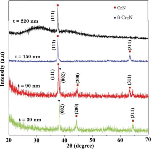
Figure 1 shows the XRD patterns of CrN ilms with diferent thicknesses grown on Si (100) substrates. The CrN/ Si (100) ilms with thicknesses t = 30 nm was found to be hexagonal (β- Cr2N) crystal structure with preferred (002) orientation along with small orientation peaks (200) and (311), and further increasing thickness (t =150 and 220nm) the ilms were exhibited structural phase transition from hexagonal β-Cr2N with (002) orientation to (111) orientation of cubic CrN. The ilm with an intermediate thickness of 90 nm was found to have mixed phase of hexagonal β-Cr2N (002) and cubic CrN phase with fundamental peak (111) and small intensity of (200) and (311) peaks were observed. Many authors were reported in the literature, the CrN ilms exhibits structural phase transition from NaCl cubic crystal structure at room temperature to orthorhombic structure at Neel temperature16. In this present study, the CrN/Si ilms exhibited structural transition due to the variation of thickness. Nevertheless, we have noticed the mixed CrN phase for the 90 nm ilm due to structural transition from the lower thickness of hexagonal β-Cr2N phase to higher thickness of cubic CrN phase. This structural transition could be due to the lattice misit of CrN phase w.r.t to substrate. In order to investigate the micro structural properties, we studied
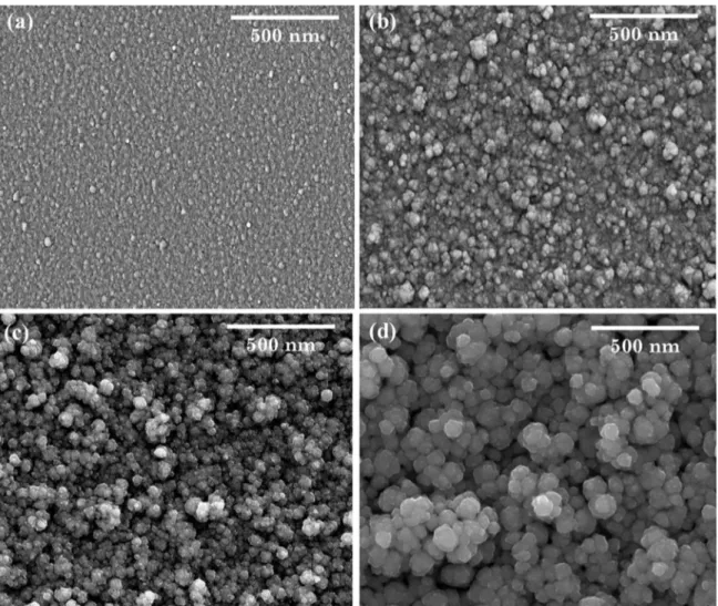
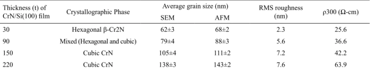
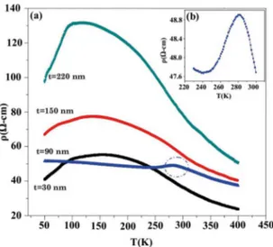
the scanning electron microscope (SEM) and atomic force microscopy (AFM) analysis for all deposited CrN/Si (100) ilms. Figure 2(a)-(d) and Figure 3(a)-(d) depicts the scanning electron microscope (SEM) and atomic force microscope (AFM) microstructures of various thicknesses (t = 30, 90, 150 and 220 nm) of CrN/Si (100) ilms, respectively. The SEM and AFM images show that the CrN thickness efectively changes the microstructure of the ilms. All deposited ilms were homogeneous and crack-free. Both SEM and AFM microstructures replicate an increase in grain size with increasing of CrN thickness and all the ilms are spherical grains in nature. The values of average grain size (for both SEM and AFM) and root mean square (RMS) surface roughness were given in Table 1. The grain size and RMS roughness of the ilms were observed to increase with the increasing CrN thickness. Figure 4 (a) shows electrical resistivity as a function of temperature ρ (T) measured between 50 K to 400 K of all CrN/Si (100) ilms with diferent thicknesses. Thickness of 150 nm CrN/Si ilm was polycrystalline cubic structure in nature conformed from XRD results. In the ρ (T) curve, the t =90 nm CrN/Si ilm resistivity (ρ) slightly decreasing with increasing T between 50 and 250 K, showing semiconducting behaviour with dρ/dT < 0. At 250 K, ρ begins to increase sharply and reaches 284 K, it indicates the metallic behvior with dρ/dT > 0. Further increasing the
Figure 2. SEM images of (a) t = 30 nm, (b) t = 90 nm, (c) t = 150 nm and (d) t = 220 nm CrN/Si (100) ilms.
temperature from 284 K to 400 K, the ρ decreasing sharply showed the semiconducting behaviour, this could be attributed
to the presence of a band gap or carrier localization due to grain boundaries or N-vacancies17,18. The room temperature
resistivity is 36.6 Ω-cm, this is within the wide range of
previously reported values, 3× 10⁻⁴ to 600 Ω-cm, obtained
from polycrystalline CrN thin ilms19. The resistivity shows the discontinuity at around 250-284 K (marked in curve), as shown in Figure 4(b), which is associated with a structural phase transition. This discontinuity could be occurred due to the grain boundary changes in the ilm and as well as changing in the shape and volume of the unit cell during
phase transition20. Most polycrystalline CrN ilms exhibits
the phase transitions due to distort the individual grains in
diferent directions and the associated volume reduction would provide suicient space within the microstructure for grain boundary slide. To study the electrical transport mechanism of this ilm, we have itted the curve above the Neel temperature (TN) of CrN in the semiconducting (284-400 K) region, as shown in Figure 5.
By using an activation law
*
exp
/
T
0E
g2
KT
1
t
Q
V
=
t
Q
V
Q
V
we have calculated the slope of the curve equal to Eg/2K and corresponding Eg value 80 meV with ρ0=4.59 × 10
-3 Ω cm, the room temperature resistivity ρ300 K = 36.6 Ω-cm. The Eg value is consistent with these previously reported values and range from 48 to 81 meV14.
Further, the thickness of t= 30, 1 50 and 220 nm CrN ilms deposited on Si (100) substrates shows the resistivity decreases monotonically with increasing temperature range 50- 400 K, and shows no discontinuity at around 280 K, suggesting no phase transition. This is in contrast to some
earlier reported authors4,21. Here, XRD results shows that
t = 30 nm CrN ilm is a hexagonal crystal structure and not shown any structural phase transition in ρ (T) curve,
this could be due to the lack of appropriate N-vacancy
Figure 3. AFM microstructures of (a) t = 30 nm, (b) t = 90 nm, (c) t = 150 nm and (d) t = 220 nm CrN/Si (100) ilms.
Table 1. Various parameters of diferent thicknesses of CrN/Si(100) ilms
Thickness (t) of
CrN/Si(100) ilm Crystallographic Phase
Average grain size (nm) RMS roughness
(nm) ρ300 (Ω-cm)
SEM AFM
30 Hexagonal β-Cr2N 62±3 68±2 2.3 25.6
90 Mixed (Hexagonal and cubic) 79±4 88±3 5.6 36.6
150 Cubic CrN 105±4 111±2 7.2 42.2
220 Cubic CrN 138±3 143±2 7.6 63.9
only semiconducting behaviour entire temperature range. The resistivity of the ilm fabricated with thickness t = 220 nm ilm also exhibiting semiconducting behaviour. Among all the thicknesses, t = 90 nm CrN/Si ilm only shown the
phase transition, this thickness is called critical thickness of
the CrN ilm deposited on Si (100) substrate. The structure of t = 220nm CrN/Si ilm having the perfect lattice with cubic (111) single orientation, due to perfect lattice, makes the transition is very diicult; this could be one of the factor to
variable-Figure 4. Resistivity versus temperature ρ(T) curves of diferent thicknesses of CrN/Si (100)ilms.
4. Conclusions
In the summery, we have successfully deposited CrN thin ilms for a thickness t in the 30-220 nm range onto Si (100) substrate and investigated the structural and electrical properties. Deposited CrN/Si (100) ilms have showed structural transition from hexagonal phase (β-Cr2N) to cubic phase (CrN) with the increasing in ilm thickness. From ρ (T) measurements, the thickness of 150 nm CrN/Si (100) ilm shown the metal-semiconductor phase transition at around 250 K with energy band gap (Eg) 81 meV in semiconducting region. Further, AFM microstructures shown CrN/Si ilms grain size increases with increasing of thickness.
5. References
1. Wiklund U, Bromark M, Larsson M, Hedenqvist P, Hogmark S. Cracking resistance of thin hard coatings estimated by four-point bending. Surface and Coatings Technology. 1997;91(1-2):57-63. 2. Nouveau C, Djouadi MA, Banakh O, Sanjinés R, Lévy F. Stress and structure proiles for chromium nitride coatings deposited by r.f. magnetron sputtering. Thin Solid Films. 2001;398-399:490-495. 3. Shah HN, Jayaganthan R, Kaur D, Chandra R. Inluence of
sputtering parameters and nitrogen on the microstructure of chromium nitride thin ilms deposited on steel substrate by direct-current reactive magnetron sputtering. Thin Solid Films. 2010;518(20):5762-5768.
4. Corliss LM, Elliott N, Hastings JM. Antiferromagnetic Structure of CrN. Physical Review. 1960;117(4):929.
5. Ibberson RM, Cywinski R. The magnetic and structural transitions in CrN and (CrMo)N. Physica B: Condensed Matter. 1992;180-181(Pt 1):329-332.
6. Gall D, Shin CS, Haasch RT, Petrov I, Greene JE. Band gap in epitaxial NaCl-structure CrN (001) layers. Journal of Applied Physics. 2002;91(9):5882.
7. Shah HN, Jayaganthan R, Pandey AC. Nanoindentation study of magnetron-sputtered CrN and CrSiN coatings. Materials &Design. 2011;32(5):2628-2634.
8. Subramanian B, Prabhakaran K, Jayachandran M. Inluence of nitrogen low rates on materials properties of CrNx ilms grown
by reactive magnetron sputtering. Bulletin of Materials Science. 2012;35(4):505-511.
9. Martinez E, Sanjinés R, Banakh O, Lévy F. Electrical, optical and mechanical properties of sputtered CrNy and Cr1− xSixN1.02thin
ilms. Thin Solid Films. 2004;447-448:332-336.
10. Mayrhofer PH, Rovere F, Moser M, Strondl C, Tietema R. Thermally induced transitions of CrN thin ilms. ScriptaMaterialia. 2007;57(3):249-252.
11. Inumaru K, Koyama K, Imo-oka N, Yamanaka S. Controlling the structural transition at the Néel point of CrN epitaxial thin ilms using epitaxial growth. Physical Review B. 2007;75(5):054416. 12. Ney A, Rajaram R, Parkin SSP, Kammermeier T, Dhar S.
Magnetic properties of epitaxial CrN ilms. Applied Physics Letters. 2006;89(11):112504.
Figure 5. Fitting curve of t = 90 nm CrN/Si (100) in the semiconducting (284-400 K) region.
range hopping (VRH) conduction mechanism with ρ α T -1/4 22,23. Mott VRH describes well the temperature dependence of ρ for approximately 50-230 K, for all thicknesses t = 30, 150 and 220 nm of CrN ilms. This suggests a hopping like conduction mechanism is itted for our semiconducting CrN thin ilms in the region of 50-230 K. When the ilm thickness is decreased, the relative impact of the strain generated at the ilm-substrate interface becomes increasingly important
and result in the change of electrical properties of these
ilms. On the other hand, AFM micrographs indicated that the thicker ilms have larger grain size, the larger grain
size results in a lower density of grain boundaries, which behaves as traps for free carriers and barriers for carrier
transport in the ilm24. Hence, an increase in grain size can
cause a decrease in grain boundary scattering, which leads
13. Filippetti A, Pickett WE, Klein BM. Competition between magnetic and structural transitions in CrN. Physical Review B. 1999;59(10):7043.
14. Constantin C, Haider MB, Ingram D, Smith AR. Metal/ semiconductor phase transition in chromium nitride (001) grown by rf-plasma-assisted molecular-beam epitaxy. Applied Physics Letters. 2004;85(26):6371-6373.
15. Zhou Z, Luo S, Wang Y, Ai Z, Liu C, Wang D, et al. Room temperature ferromagnetism and hopping transport in amorphous CrN thin ilms. Thin Solid Films. 2011;519(6):1989-1992. 16. Zhang XY, Chawla JS, Deng RP, Gall D. Epitaxial suppression
of the metal-insulator transition in CrN. Physical Review B. 2011;84(7):073101.
17. Duan XF, Mi WB, Guo ZB, Bai HL. A comparative study of transport properties in polycrystalline and epitaxial chromium nitride ilms. Journal of Applied Physics. 2013;113(2):023701. 18. Emery C, Chourasia AR, Yashar P. A study of CrNx thin ilms
by X-ray photoelectron spectroscopy. Journal of Electron
Spectroscopy and Related Phenomena. 1999;104(1-3):91-97.
19. Mott N. On metal-insulator transitions. Journal of Solid State Chemistry. 1990;88(1):5-7.
20. Ruden A, Restrepo-ParraE, PaladinesAU, Sequeda F. Corrosion resistance of CrN thin ilms produced by dc magnetron sputtering.
Applied Surface Science. 2013;270:150-156.
21. Elangovan T, Kuppusami P, Thirumurugesan R, Ganesan V, Mohandas E, Mangalraj D. Nanostructured CrN thin ilms prepared by reactive pulsed DC magnetron sputtering. Materials Scinece and Engineering B. 2010;167(1):17-25.
22. Mott NF, Davis EA. Electronic Processes in Non-Crystalline Materials. 2nd ed. Oxford: Clarendon Press; 1979.
23. Mott NF. Metal-Insulator Transitions. 2nd ed. Bristol: Taylor
& Francis; 1990.