Development
of p
-
type oxide semiconductors
based on tin oxide
and
its
alloys: application
to thin film transistors
Dissertação para obtenção do Grau de Doutor em Nanotecnologias e Nanociências
Orientador: Doutora Elvira Maria Correia Fortunato, Professora
Catedrática, Faculdade de Ciências e Tecnologia da
Universidade Nova de Lisboa
Co-orientador: Doutor Rodrigo Ferrão de Paiva Martins, Professor
Catedrático, Faculdade de Ciências e Tecnologia da
Universidade Nova de Lisboa
Júri:
Presidente: Professor Doutor Nuno Manuel Robalo Correia Arguentes: Professora Doutora Florinda Mendes da Costa
Professor Doutor Henrique Leonel Gomes
Vogais: Professor Doutor Albano Augusto Cavaleiro Rodrigues de Carvalho
Professora Doutora Ana Maria Botelho Rego Professor Doutor Pedro Miguel Cândido Barquinha
i
Development of p-type oxide semiconductors
based on tin oxide and its alloys: application to
thin film transistors
Dissertação para obtenção do Grau de Doutor
em Nanotecnologias e Nanociências
Novembro de 2014
Orientador: Doutora
Elvira
Maria
Correia
Fortunato,
Professora
Catedrática, Faculdade de Ciências e Tecnologia da
Universidade Nova de Lisboa
Co-orientador:: Doutor Rodrigo Ferrão de Paiva Martins, Professor,
Catedrático Faculdade de Ciências e Tecnologia da
Universidade Nova de Lisboa
Júri:
Presidente: Professor Doutor Nuno Manuel Robalo Correia Arguentes: Professora Doutora Florinda Mendes da Costa
Professor Doutor Henrique Leonel Gomes
Vogais: Professor Doutor Albano Augusto Cavaleiro Rodrigues de Carvalho
iii
Development of p-type oxide semiconductors based on tin oxide and its alloys: application to thin film transistors
Copyright © Ana Raquel Xarouco de Barros, Faculdade de Ciências e Tecnologia, Universidade Nova de Lisboa.
v
ACKNOWLEDGMENTS
It was a great privilege to be part of this creative and prestigious research group during these four years, where an environment of great fellowship and friendship persists and in which this work was only possible with the support of several people that I would like to sincerely thank.
First and foremost, I would like to thank Professor Elvira Fortunato, for allowing me to work in this research group, for the form she guided my work and for all the support and suggestions, that have contributed to my personal and professional development. I am grateful for her interest, encouragement and friendship.
To Professor Rodrigo Martins, for the constant interest shown in my work and for the incentive and help on understanding the results.
To Professor Pedro Barquinha, a special and grateful thank. Without his knowledge and ideas, this work would not have taken the same direction. His unlimited support, motivation and friendship were essential to my development as a researcher, a team member and as a person. You are our “special one”.
To my friend and officemate, Dipl. Ing. Jonas Deuermeier, for the XPS measurements done at Darmstad and for all the long talks about science, for the friendship and for being so patient to me during the writing process. Thank you for teaching me that “stress” should not exist in our live. For all the true moments of friendship, fun and support, I must thank to MSc Mafalda Costa, MSc Paulo Duarte, MSc Sónia Pereira, MSc Alexandra Gonçalves, MSc Andreia Araújo and MSc Nuno Neves. Their friendship was essential during this journey.
To Dr. Joana Vaz Pinto, for the major help with RBS characterization, the long talks about physics and her friendship.
To past and present co!workers: MSc Bruno Veigas, MSc. Daniela Salgueiro, MSc. Ana Catarina Santos, Professor Luís Pereira, Dr. Elangovan Elamurugu, Dr. Vítor Figueiredo, MSc. Diana Gaspar, MSc. Tiago Mateus, MSc. António Vicente, MSc. Joana Neto, Dr. Pawel Wojcik, MSc. Iwona Bernacka, Dr. Suman Nandy, Dr. Ana Pimentel, Dr. Daniela Nunes, Dr. Rita Braquinho, MSc. Lídia Santos, Dr. Sergej Filonovich, MSc Ana Rovisco, MSc Jorge Martins and others that probably I did not mention. Your help was essential! Thank you all!
vi
To the technicians who work or have worked in CENIMAT, CEMOP and DCM: Carlos Alcobia, Manuel Quintela, Ricardo Ferreira and Salomão Lopes for the help solving the technical problems related with production and characterization systems.
To all my friends, that always supported and motivated me, and understand my unavailability during these years.
To the most important persons in my life: my parents and my sister that I love unconditionally. For all their love and for always support and believe in me! I own them all that I am and today and no words could ever be enough to thank them!
To Ricardo Guedes, that although was not present from the very beginning, his support, companionship and love were essential in closing this chapter of my life!
vii
ABSTRACT
In spite of the recent p-type oxide TFTs developments based on SnOx and CuxO, the results
achieved so far refer to devices processed at high temperatures and are limited by a low hole mobility and a low On-Off ratio and still there is no report on p-type oxide TFTs with performance similar to n-type, especially when comparing their field-effect mobility values, which are at least one order of magnitude higher on n-type oxide TFTs. Achieving high performance p-type oxide TFTs will definitely promote a new era for electronics in rigid and flexible substrates, away from silicon. None of the few reported p-channel oxide TFTs is suitable for practical applications, which demand significant improvements in the device engineering to meet the real-world electronic requirements, where low processing temperatures together with high mobility and high On-Off ratio are required for TFT and CMOS applications.
The present thesis focuses on the study and optimization of p-type thin film transistors based on oxide semiconductors deposited by r.f. magnetron sputtering without intentional substrate heating. In this work several p-type oxide semiconductors were studied and optimized based on undoped tin oxide, Cu-doped SnOx and In-doped SnO2.
The influence of the deposition parameters, such as the percentage of oxygen and the deposition pressure and post deposition annealing treatments (up to 200 °C) parameters was investigated in order to optimize the properties of the p-type thin films. The detailed study of the material was accomplished through various techniques of characterization of their electrical and optical properties, crystal structure, chemical composition, topology and morphology.
The obtained undoped SnOx thin films showed p-type conduction for a narrow percentage of
oxygen, between 2.5% and 4%, after an annealing treatment at 150 °C and 200 °C. The thin films have a mixture of both tetragonal β-Sn and α-SnO phases, mobilities between1.6 cm2/Vs and 2.6 cm2/Vs and a carrier concentration between 1016 and 1017 cm-3. TFTs produced with this material were optimized presenting very good electrical performances, with On-Off ratio ~104, µFE up to 3.5
cm2/Vs and Vth between -0.41 V and 15 V. The influence of the dielectric was also studied and
leading to new results. Depending on the gate dielectric used, n-, p-type and ambipolar devices were obtained for the same semiconductor deposition conditions.
Doping SnOx with Cu also results in transparent p-type oxide semiconductors with mobilities
between 1.6 cm2/Vs and 2.6 cm2/Vs and a carrier concentration between 1016 and 1017 cm-3. When applied as active layer, resulted in poor performance thin film transistors, with lower On-Off ratio and the higher Vth, despite µFE increased.
When doping the SnO2 films with In, p-type conduction was achieved without the need of the
viii
ix
RESUMO
Apesar dos recentes desenvolvimentos em TFTs tipo-p, baseados em SnOx e CuxO, os
resultados obtidos até agora referem-se a dispositivos produzidos a temperaturas elevadas, cuja principal limitação é a baixa mobilidade dos portadores de carga maioritários, buracos, e baixa razão On-Off. Sendo que ainda não se encontra na literatura aritogs de TFTs tipo-p com desempenho semelhante a TFTs tipo-n, produzir TFTs tipo-p a baixa temperatura com elevado desempenho, vai certamente iniciar uma nova era para a electrónica em substratos rígidos e flexíveis onde temperaturas de processo baixas, elevada mobilidade e elevado rácio On-Off são necessários para aplicações em TFTs e CMOS.
Esta tese, foca-se no estudo e optimização de TFTs baseados em óxidos semicondutores tipo-p depositados por pulverização catódica reactiva de rádio frequência assistida por magnetrão sem aquecimento intencional do substrato. Neste trabalho foram estudados e otimizados vários óxidos semicondutores tipo-p de SnOx não dopado, SnOx dopado com Cu, e SnO2 dopado com
In. A influência dos parâmetros de deposição, tais como a quantidade de oxigénio na câmara de deposição, a pressão de deposição e o recozimento efectuado após a deposição (até 200 °C), foi estudada de forma a optimizar as propriedades dos óxidos semicondutores transparentes. O estudo detalhado do material foi realizado através de várias técnicas de caracterização, tendo inferido as propriedades eléctricas, ópticas, estruturais, composição química, e morfologia. Os filmes de SnOx obtidos apresentam condução tipo-p para uma percentagem de oxigénio
entre 2.5% e 4%, após um tratamento térmico de 150 °C – 200 °C. Os filmes apresentam uma mistura de fases de β-Sn e α-SnO, apresentando mobilidades entre 1,6 cm2/Vs e 2,6 cm2/Vs, e uma concentração de portadores entre 1016 e 1017 cm-3.
Após a obtenção do óxido semicondutor tipo-p, produziram-se os TFTs. Obtiveram-se TFTs a funcionar nos diferentes modos, de depleção e enriquecimento, com Vth de -0,41 V a 15 V, rácio
On-Off ratio ~104 e µFE até 3.5 cm2/Vs . A influência do dieléctrico no desempenho do dispositivo
também foi estudada, tendo sido obtidos novos e promissores resultados. Dependendo do dieléctrico utilizado, foram obtidos transístores a tipo-n, tipo-p e ambipolares, para a mesma condição de deposição da camada activa.
Dopar SnOx com Cu também resultou em óxidos semicondutores tipo-p com mobilidades entre
1.6 cm2/Vs e 2.6 cm2/Vs e N entre 1016 e 1017 cm-3. Os transístores com base neste material apresentam, de um forma geral, um pior desempenho, com um rácio On-Off inferior e maior Vth,
apesar do aumento na µFE.
Ao dopar SnO2 com In, obtiveram-se semicondutores tipo-p, sem a necessidade de qualquer
x
xi
SYMBOLS
%Cu - percentage of copper defined by (Cu/(Cu+Sn)) %In - percentage of copper defined by (In/(In+Sn)) percentage of oxygen content in the Ar+O2 mixture
!
!"!magnetic!field!vector
E - electric field vector A – Area
c - Speed of light (= 3.0 × 10⁸ m/s) Ci - Areal capacitance
D - Crystallite size dd - Dielectric thickness
dhkl - Inter-planar spacing
ds - Oxide semiconductor thickness
E - Electric field
Ea - Thermal activation energy
Ec - Conduction band
EF - Fermi level
EG – Bandgap
Eopt - Optical band-gap (eV)
gd – Condutance
gm – Transcondutance
h - Planck’s constant (= 6.626 × 10⁻³⁴ J·s) I - Current
xii IGS - Gate leakage current
Ioff - IDS at off state
Ion - IDS at on state
J - Current density k - Extinction coefficient L - Channel length n - Refractive index
N - Free carrier concentration Ns - Sheet carrier density
On-Off ratio - TFT IDS on-to-off ratio
pd - Deposition pressure
Prf - rf power density
q - Elementary charge of a particle (1.6x10⁻¹⁹ C) RH - Hall coefficient
Rsheet - Sheet resistance
SS - Subthreshold gate voltage swing T – Transmittance
TA - Annealing temperature
V – Voltage
VDS - Drain to source voltage
VGS - Gate voltage
VH - Gate voltage
Von - Turn-on voltage
Vth - Threshold voltage
xiii
α−Absorption coefficient (/cm)
ε0 - Vacuum dielectric constant (= 8.85 × 10 -12
F/m)
εs - Dielectric constant of the semiconductor
ϑ - Bragg angle
Φ - Figure of merit
χ−Electron affinity
χ2- Error function ϕB - Barrier height
ϕG - Gate electrode work function
ϕM - Metal work function
ϕS - Semiconductor work function
κ−Dielectric constant
λ−Wavelength of electromagnetic wave
µ −Mobility
µ FE - Field-effect mobility
µ SAT - Saturation mobility
µeff - Effective mobility
ρ−Electrical resistivity
σ−Electrical conductivity
υ−Frequency of electromagnetic wave
xv
ABBREVIATIONS
AFM Atomic Force Microscopy ALD Atomic Layer Deposition ATO Antimony!doped Tin Oxide CBM Conduction band minimum
CEMOP Centro de Excelência de Microelectrónica e Optoelectrónica de Processos CENIMAT Centro de Investigação de Materiais
CVD Chemical Vapor Deposition EDS Energy Dispersive X-ray FPD Flat Panel Display
FWHM Full Width at Half Maximum GIZO Gallium Indium Zinc Oxide
I3N Instituto de Nanoestruturas, Nanomodelação e Nanofabricação IPA Isopropilic Alcohol
ITN Instituto Tecnológico e Nuclear ITO Indium Tin Oxide (Sn-doped In2O3)
KP Kelvin Probe
LCD Liquid Crystal Display LED Light Emitting Diode
MIS Metal!Insulator!Semiconductor
MOSFET Metal!Oxide!Semiconductor Field!Effect Transistor NIR Near Infrared
xvi PVD Physical Vapor Deposition
r.f. radio!frequency RBS
Rutherford Backscattering Spectroscopy
RMS Root-mean-square
sccm Standard cubic centimeters per minute SEM Scanning Electron Microscopy
SMU Source"Monitor Unit
SPA Semiconductor Parameter Analyzer STM Scanning Tunneling Microscopy TCLC Trap Charged Limited Current TCO Transparent Conducting Oxide TFT Thin-Film Transistor
TSO Transparent Semiconductor Oxide UV Ultra!Violet
VBM Valence Band Maximum VRH Variable Range Hopping
xvii
Table of Contents
ACKNOWLEDGMENTS...v!
ABSTRACT...vii!
RESUMO...ix!
SYMBOLS...xi!
ABBREVIATIONS...xv!
Table.of.Contents...xvii!
List.of.Figures...xxi!
List.of.Tables...xxix!
1.!
MOTIVATION,.OBJECTIVE.AND.STRUCTURE.OF.THE.DISSERTATION...3!
!
Motivation...3! 1.1.!
Objectives...4! 1.2.!
Structure.of.the.dissertation...4! 1.3.!
References...5! 1.4.2.!
TRANSPARENT.OXIDE.SEMICONDUCTORS,.THIN
FILM.TRANSISTORS...11!
!
General.concepts...11!2.1.
!
PUtype.oxide.semiconductors...15!2.2.
!
ThinFilm.Transistors.(TFTs)...19!2.3.
!
TFT!structure!and!operation!...!19!
2.3.1.
!
TFT!operation!...!23!
2.3.2.
!
References...27! 2.4.3.!
THIN.FILMS.AND.DEVICES:.DEPOSITION.AND.CHARACTERIZATION.TECHNIQUES...41!
!
ThinUfilm.and.TFT.processing...41! 3.1.!
Sputtering!...!41!
3.1.1.
!
Electron!beam!physical!vapor!deposition!...!45!
3.1.2.
!
PostAdeposition!annealing!...!48!
3.1.3.
!
Photolithography!...!49!
3.1.4.
!
Thin.film.characterization.techniques...52!xviii
!
Electrical!characterization!...!54!
3.2.2.!
Structural!and!morphological!characterization!...!61!
3.2.3.!
Compositional!Characterization!...!65!
3.2.4.!
Optical!characterization!...!68!
3.2.5.!
Thinfilm.transistor...69! 3.3.!
Currentvoltage!measurements!...!69!
3.3.1.!
Stress!measurements!...!70!
3.3.2.!
References...71! 3.4.4.!
TRANSPARENT.P
TYPE.OXIDE.SEMICONDUCTOR.PRODUCED.BY.SPUTTERING...75!
!
Oxide.semiconductors.based.on.SnO...75! 4.1.!
Deposition!Parameters!...!75!
4.1.1.!
Dependence!of!the!growth!rate!on!the!deposition!parameters!...!76!
4.1.2.!
Structural!and!morphological!properties!...!77!
4.1.3.!
Compositional!analysis!...!82!
4.1.4.!
Optical!properties!...!86!
4.1.5.!
Electrical!properties!...!89!
4.1.6.!
Oxide.semiconductors.based.on.CuUdoped.SnOx...95! 4.2.!
Deposition!parameters!...!95!
4.2.1.!
Dependence!of!the!growth!rate!on!the!deposition!parameters!...!95!
4.2.2.!
Compositional!analysis!...!96!
4.2.3.!
Structural!and!morphological!properties!...!98!
4.2.4.!
Optical!properties!...!101!
4.2.5.!
Electrical!properties!...!104!
4.2.6.!
Oxide.semiconductors.based.on.InUdoped.SnO2...105! 4.3.!
Deposition!parameters!...!105!
4.3.1.!
Electrical!properties!...!105!
4.3.2.!
Compositional!analysis!...!107!
4.3.3.!
Structural!and!morphological!properties!...!110!
4.3.4.!
Optical!properties!...!111!
4.3.5.!
Conclusions...113! 4.4.!
References...117! 4.5.5.!
TRANSPARENT.P
TYPE.THINUFILM.TRANSISTORS...123!
xix
!
Influence!of!the!deposition!and!postAdeposition!parameters!on!the!electrical! 5.1.2.properties!of!TFTs!...!124
!
!
Influence!of!gate!dielectric!on!the!electrical!properties!of!TFTs!...!136!
5.1.3.!
Electrical!stability!...!147!
5.1.4.!
TFTs.with.CuUdoped.SnOx.channel...150! 5.2.!
Process!flow!and!device!structure!...!150!
5.2.1.!
Influence!of!the!deposition!and!postAdeposition!parameters!on!the!electrical! 5.2.2.properties!of!Cu!doped!SnOx!TFTs!...!151
!
!
Conclusions...154! 5.3.!
References...155! 5.4.6.!
FINAL.CONCLUSIONS.AND.FUTURE.PERSPECTIVES...165!
!
Conclusions...165! 6.1.!
pAtype!oxide!semiconductors!...!165!
6.1.1.!
PAtype!oxide!semiconductor!based!thinAfilmAtransistor!...!168!
6.1.2.xxi
List of Figures
xxii
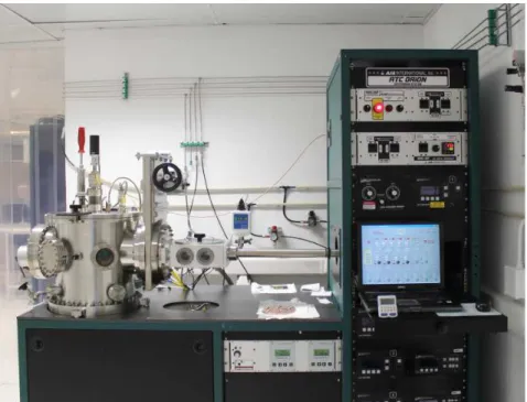
Figure 3.10. Picture of the yellow zone existing at CEMOP’s clean room. ... 50
!
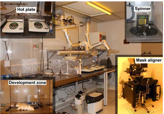
Figure 3.11. Process flows showing the main steps of conventional photolithography. ... 52!
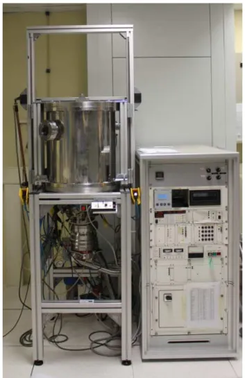
Figure 3.12. Picture of Ambios XP-200 existing at CENIMAT. ... 53!
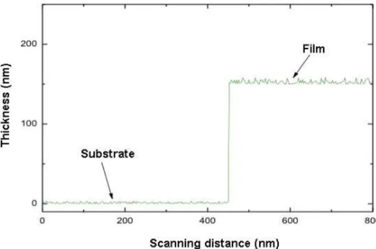
Figure 3.13. Typical step height corresponding to a 150 nm film thickness deposited on a glass substrate. ... 53!
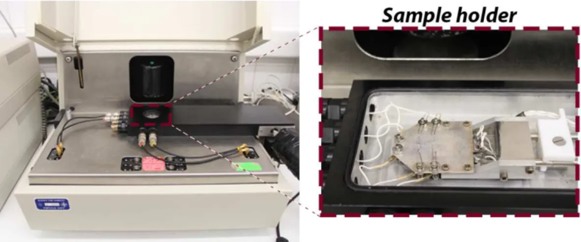
Figure 3.14. Biorad HL 5500 Hall effect system existing at CENIMAT, New University of Lisbon. ... 54!
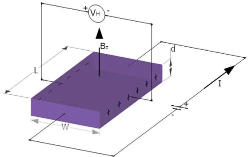
Figure 3.15. Illustration of the experimental setup allowing the observation of Hall effect. ... 55!
Figure 3.16. Illustration of the definition of sheet resistance. ... 56!
Figure 3.17. Techniques to measure electrical resistance of thin films. a) four point method to measure sheet resistance (b) Van der Pauw method to measure the resistivity with arbitrary geometries. ... 57!
Figure 3.18. Van der Pauw geometry used for the thin films Hall effect measurements. ... 57!
Figure 3.19. Van der Pauw method to measure RA and RB. ... 58!
Figure 3.20. Van der Pauw method to measure RA and RB. ... 59
!
xxiii
CEMOP, New University of Lisbon. ... 68
!
Figure 3.32. Microprobe Cascade MicroTech M150 and Agilent 4155C existing at CENIMAT; New University of Lisbon. ... 69!
Figure 3.33. Microprobe Cascade MicroTech M150 and Agilent 4155C existing at CENIMAT; New University of Lisbon. ... 70!
Figure 4.1. Growth rate as function of %O2 and pd. ... 77!
Figure 4.2. XRD diffractograms for the SnOx films deposited at pd=0.2 Pa and annealed at 200 °C
as a function of %O2 ... 78
!
Figure 4.3. XRD diffractograms for the SnOx films annealed at 200 °C deposited at different
deposition pressures and oxygen content. ... 78
!
Figure 4.4. AFM, a) to e) and SEM, f) to j) images of the films deposited at pd= 0.2 Pa, TA= 200°C for different %O2. ... 79
!
Figure 4.5. Dependence of surface roughness and grain size with oxygen content for the films deposited at pd= 0.2 Pa and annealed at 200 °C. ... 80
!
Figure 4.6. XRD diffractograms for the SnOx films deposited at pd=0.2 Pa for different annealingtemperatures and oxygen content. ... 81
!
Figure 4.7. Dependence of crystallite size with annealing temperature for the films deposited at pd= 0.2 Pa different %O2. ... 81!
Figure 4.8. SEM and AFM images of the films deposited at pd= 0.2 Pa, %O2=2.5 %, as deposited
and TA= 200 °C. ... 82
!
Figure 4.9. XPS survey spectra of tin oxide films as deposited and annealed prepared by reactive magnetron sputtering. ... 83
!
Figure 4.10. O1s, Sn 3d3/2 and Sn 3d5/2 XPS spectra of SnOx thin film as deposited and annealedat 200 °C. ... 83
!
Figure 4.11. XPS spectra of Sn 3d (a) as deposited and (b)annealed for the SnOx films. Smoothlines are representing fitting data. ... 84
!
Figure 4.12. Valence band spectra of SnOx films as deposited and annealed at TA=200 °C. ... 85!
Figure 4.13. Optical transmittance spectra of the SnOx films with different content of oxygen a) as
xxiv
Figure 4.14. Picture of the thin films annealed at TA=200 °C with a %O2 of a)2.5%, b)3.0%, c)
3.5% and d) 4%. ... 87
!
Figure 4.15. Picture of the thin films with 120 nm thickness with a %O2=2.5% a) As deposited andb) Annealed at TA=200 °C and c) With 12 nm thickness annealed at TA=200 °C. ... 88
!
Figure 4.16. (αhν)2 vs photon energy (hν) spectra for the films a) as deposited and b) annealed at 200 °C; c) calculated optical bandgap as a function of oxygen content for the thin films. ... 89
!
Figure 4.17. Variation of resistivity (ρ), mobility (µ) and carrier concentration (n) as a function of the oxygen content (%O2). ... 90!
Figure 4.18. Variation of crystallite (D) size and mobility (µ)a function of the oxygen content (%O2). ... 91
!
Figure 4.19. Variation of resistivity (ρ), mobility (µ) and carrier concentration (n) as a function of the oxygen content (%O2). ... 92
!
Figure 4.20. Variation of resistivity (ρ), mobility (µ) and carrier concentration (n) as a function of the annealing temperature(TA). ... 93
!
Figure 4.21. Temperature dependent dark conductivity for p-type SnOx films with different %O2.
... 94
!
Figure 4.22. Growth rate as function of %Cu. ... 96!
Figure 4.23. Atomic concentrations obtained by EDS of Cu, on Cu doped SnOx thin films. ... 96!
Figure 4.24. RBS spectrum for the Cu-doped SnOx films deposited at pd=0.2 Pa as a function of
%Cu a) as deposited and b) annealed at 200 °C. ... 97
!
Figure 4.25. RBS diffractograms for the Cu-doped SnO films deposited as deposited and annealed at 200 °C for a) %Cu=4.0 % and b) %Cu=7.0 %. ... 98!
Figure 4.26. XRD diffractograms for the Cu-doped SnOx films deposited at pd=0.2 Pa as axxv
f) - j) annealed at TA= 200 °C; and k) - o) AFM images annealed of the films annealed at
TA= 200 °C ... 101
Figure 4.30. Optical transmittance spectra of the SnOx films with different content of copper a) as
deposited and b) annealed at 200 °C. ... 102
!
Figure 4.31. Picture of the thin films as deposited with a %Cu of a) 0 %, b)4.0 %, c) 5.5 %, d) 7.0 % and e) 9.0 % ... 102!
Figure 4.32. Picture of the thin films annealed at TA=200 °C with a %Cu of a) 0 %, b)4.0 %, c) 5.5%, d) 7.0 % and e) 9.0 % ... 103
!
Figure 4.33. (αhν)2 vs photon energy (hν) spectra for the films a) as deposited and b) annealed at 200 °C and c) calculated optical bandgap as a function of copper content for the thin films. ... 103!
Figure 4.34. Variation of resistivity (ρ), mobility (µ) and carrier concentration (n) as a function of copper content (%Cu). ... 104!
Figure 4.35. Variation of a) resistivity (ρ),b) mobility (µ) and c) carrier concentration (n) as a function %In for different %O2. ... 106!
Figure 4.36. Atomic concentrations obtained by EDS of In, on In-doped SnO2 thin films. ... 107
!
Figure 4.37. XPS survey spectra of tin oxide films as deposited and annealed prepared by reactive magnetron sputtering. ... 108
!
Figure 4.38. O1s, Sn 3d3/2,Sn 3d5/2 and In 3d5/2 XPS spectra of n-type and p-type In-doped SnO2films. ... 108
!
Figure 4.39. XPS spectra of Sn 3d5/2 for (a) n-type and (b)p-type In-doped SnO2 and for c) SnOxp-type. Smooth lines are representing fitting data. ... 109
!
Figure 4.40. Valence band spectra of SnOx and In-doped SnO2 films. ... 110!
Figure 4.41. XRD diffractograms for the In-doped SnO2 films deposited at different %O2 and %In.
... 110
!
Figure 4.42. a) – c) SEM and f) – h) AFM images of In.doped SnO2 films with %O2=5.0 – 7.0 %and %In=15 – 26%. ... 111
!
Figure 4.43. Optical transmittance spectra of In-doped SnO2 films with different content of In fora) %O2=5 % and b) %O2=7 %. ... 112
!
xxvi
Figure 4.45. (αhν)2 vs photon energy (hν) spectra of In-doped SnO2 films with different %In for a)
%O2=5 % and b) %O2=7 %; c) calculated optical bandgap as a function of In content. ... 113
!
Figure 5.1. Masks used for the fabrication of bottom gate thin film transistors a) channel and b) source and drain patterning. ... 123
!
Figure 5.2. Process flow used to produce TFTs based on SnOx and schematic of the bottom gatedevice structure. ... 124
!
Figure 5.3. a) transfer curves and the c) variation of the main electrical characteristics for TFTs deposited at different percentages of oxygen, a deposition pressure of 0.2 Pa and 12 nm SnOxchannel thickness, annealed at 200 °C. Vth was calculated from the linear extrapolation of IDS-VGS
curves at b) at the linear regime. ... 125
!
Figure 5.4. Output curves for the TFTs deposited at different percentages of oxygen, a deposition pressure of 0.2 Pa and 12 nm SnOx channel thickness, annealed at 200 °C. ... 126!
Figure 5.5. Transfer curves measured in double sweep to access the hysteresis magnitude for the TFTs deposited at different percentages of oxygen, a deposition pressure of 0.2 Pa and 12 nm SnOx channel thickness, annealed at 200 °C. ... 127
!
Figure 5.6. a) Transfer curves and the c) variation of the main electrical characteristics for TFTs deposited at different deposition pressures, %O2= 2.5 % and ds= 12 nm, annealed at 200 °C. . 128
!
Figure 5.7. Output curves for the TFTs deposited at different depositions pressures, %O2=2.5 % and 12 nm SnOx channel thickness, annealed at 200 °C. ... 129
!
Figure 5.8. a) transfer curves and the b) variation of the main electrical characteristics for TFTs deposited at %O2= 2.5 %, pd= 0.2 Pa and ds= 12 nm, annealed at 100, 150 and 200 °C. ... 130!
Figure 5.9. Output curves for the TFTs deposited at %O2= 2.5%, pd=0.2 Pa, ts=12 nm annealead
at a)100 °C, b) 150 °C and c) 200 °C. ... 131
!
Figure 5.10. Transfer characteristics curves a) semi log and b) liner scale for the TFTs deposited with %O2= 3.5 %, pd= 0.2 Pa with different SnOx channel layer thicknesses, annealed at 200 °C.... 132
!
Figure 5.11. Output curves for the TFTs deposited with %O2= 3.5 %, pd= 0.2 Pa with a SnOxxxxvii
the TFTs deposited with different semiconductor channel thicknesses, a deposition pressure of 0.2 Pa and 12 nm SnOx channel thickness, annealed at 200 °C. ... 136
!
Figure 5.14. (a) Relation between EG and κ for for some dielectrics; (b) calculated band offsets ofoxide dielectrics on silicon ... 137
!
Figure 5.15. SEM and AFM images of the dielectrics produced. ... 141!
Figure 5.16. XRD diffractograms for multicomponent dielectrics produced with different materials. ... 142!
Figure 5.17. Influence of the dielectrics(a-c) based on ALTiO and (d-f) HfO2 in the transfercharacteristic of SnOx TFTs annealed at TA=200!°C. ... 143
!
Figure 5.18. Influence of the annealing temperature on the TFTs with gate dielectric based on a) ATO and b) HfO2 ... 145
!
Figure 5.19. Output characteristics under a) p-channel and b) n-channel operation. Transfer characteristics under a c) negative and a d) positive VDS ... 146
!
Figure 5.20. Stress (a) and recovery (b) experiments regarding device deposited with a %O2 =
2.5%, pd = 0.2 Pa and ts = 12 nm annealed at 200 °C (VD=-2 V, VGS_stress=-30 V). ... 148
!
Figure 5.21. Bias stress induced threshold voltage shift as a function of time on a logarithmic scale. (VDS=-1 V). ... 149!
Figure 5.22. Shift of threshold voltage as a function of stress time for different drain biases (VDS=0 , -1 and -5 V), constant VGS=-30 V and VDS=-1 V. ... 149
!
Figure 5.23. Process flow used to produce TFTs based on Cu-doped SnOx and schematic of the
bottom gate device structure. ... 151
!
Figure 5.24. Output curves for the TFTs deposited with %O2= 4.0 %, pd= 0.2 Pa and a Cu contentof a) 0 %, b) 4.0 %, c) 5.5 %and d) 7.0 %, annealed at 200 °C. ... 152
!
Figure 5.25. Transfer characteristics curves of the TFTs with %O2= 4 %, pd= 0.2 Pa as a functionxxix
List of Tables
Table 2.1. Candidates for a-TOS and respective electronic configuration [18]. ... 12
!
Table 2.2. Comparison between transparent n-type based TFTs and the other commercial available technologies; amorphous Si and poly-Si [7]. ... 14!
Table 4.1. Conditions used for the deposition of SnOx thin films. ... 76!
Table 4.2. Content of Sn0, Sn2+ and Sn4+ in the SnOx films as deposited and annealed. ... 85
!
Table 4.3. Activation energy calculated using the Arrhenius equation. ... 94
!
Table 4.4. Conditions used for the deposition of Cu-doped SnOx thin films. ... 95!
Table 4.5. Conditions used for the deposition of In-dopedSnO2 thin films. ... 105
!
Table 4.6. Electrical properties of the samples chosen to XPS measurements. ... 107
!
Table 4.7. Content of O, Sn and In in the n- and p- type In-doped SnO2 films and in the SnOxstructure of the thesis
!
1.!
MOTIVATION,.OBJECTIVE.AND.STRUCTURE.OF.THE.DISSERTATION...3!
!
Motivation...3! 1.1.!
Objectives...4! 1.2.!
Structure.of.the.dissertation...4! 1.3.3
1. MOTIVATION, OBJECTIVE AND STRUCTURE OF THE
DISSERTATION
Motivation
1.1.
Transparent Electronics is an emerging field of technology in which the conventional opaque electronic components are expected to be replaced by transparent electronic ones. Even though most of the conventional electronic applications require both n-type and p-type transistors, there appears relatively little effort towards the development of p-type transparent thin-film transistors (TFTs) and p-type transparent conducting oxides (TCOs) [1]–[3]. Developments on this area would enable oxide CMOS circuitry and great improvements on existing optoelectronic devices, such as OLEDs and related applications, such as flat-panel displays.
The enormous success of n-type oxides and the application of transparent conductive oxides (TCOs) as “invisible electrodes” [4], [5] and of transparent semiconductive oxides (TSOs) as active channel layers of thin-film transistors (TFTs) [6]–[9] has motivated the interest in p-type oxides for both types of applications. Indeed, p-type oxides are relevant both for TCO (as low contact resistance material for a large variety of optoelectronic devices, such as solar cells or OLEDs) and TSO (for fully transparent p-n junctions or p-type TFTs) applications. One of the major goals is to have ambipolar devices, enabling Complementary Metal Oxide Semiconductors (CMOS) architectures, for fast and low-power consumption electronics, as required when complex and integrated electronic blocks are thought to be fabricated [10] [11]
4
can be processed at low temperatures with low fabrication costs. Oxide materials are seen as one of the most promising routes to achieve this.
At present, almost all reported oxide TCOs and TSOs for TFTs are based on n-type oxides [20]– [23]. For p-type oxides, carrier conduction path (valence band) is mainly formed from the oxygen p asymmetric orbitals, which severely limits the carrier mobility. Thus, p-type oxides have very low carrier mobility compared to their n-type counterparts, which is the main obstacle in obtaining high performance TCOs and p-channel oxide TFTs. Recently much attention has been given to Cu and Sn based semiconductors[1], [3], [24]. By introducing III-family elements in these materials, such as In, doping can theoretically be achieved in order to enhance conductivity and mobility.
Objectives
1.2.
The main objective of this dissertation is to produce, study and optimize transparent sputtered p-type oxide semiconductors based on tin oxide and to apply as channel layers in thin film transistors. For this purpose, it was first studied the influence of different deposition and post deposition parameters on the structural, morphological and compositional, electrical and optical properties of the films. After its optimization, the thin films were applied as channel layer in TFTs. Besides that, it was also exploited some of the produced p-type thin films as TCOs
Structure of the dissertation
1.3.
5
References
1.4.
[1] E. Fortunato, R. Barros, P. Barquinha, V. Figueiredo, S. K. Park, C. Hwang, and R. Martins, “Transparent p-type SnOx thin film transistors produced by reactive rf magnetron
sputtering followed by low temperature annealing”, Appl. Phys. Lett., vol. 97, no. 5, 2010. [2] Y. Ogo, H. Hiramatsu, K. Nomura, H. Yanagi, T. Kamiya, M. Hirano, and H. Hosono,
“p-channel thin-film transistor using p-type oxide semiconductor, SnO”, Appl. Phys. Lett., vol. 93, no. 3, p. 032113, 2008.
[3] E. Fortunato, V. Figueiredo, P. Barquinha, E. Elamurugu, R. Barros, G. Gonçalves, S.-H. K. Park, C.-S. Hwang, and R. Martins, “Thin-film transistors based on p-type Cu2O thin
films produced at room temperature”, Appl. Phys. Lett., vol. 96, no. 19, 2010.
[4] F. Belliard, P. a. Connor, and J. T. S. Irvine, “Doped tin oxides as potential lithium ion battery negative electrodes”, Ionics (Kiel)., vol. 5, no. 5–6, pp. 450–454, Sep. 1999. [5] J. G. Partridge, M. R. Field, J. L. Peng, a Z. Sadek, J. Du Plessis, D. G. Mcculloch, K.
Kalantar-zadeh, and J. Du Plessis, “Nanostructured SnO2 films prepared from evaporated
Sn and their application as gas sensors”, Nanotechnology, vol. 19, no. 12, p. 125504, Mar. 2008.
[6] P. Barquinha, L. Pereira, G. Gonçalves, R. Martins, and E. Fortunato, “Toward High -Performance Amorphous GIZO TFTs”, J. Electrochem. Soc., vol. 156, no. 3, p. H161, 2009.
[7] E. M. C. Fortunato, P. M. C. Barquinha, A. C. M. B. G. Pimentel, a. M. F. Gonçalves, A. J. S. Marques, L. M. N. Pereira, R. F. P. Martins, and A. M. F. Gonçalves, “Fully Transparent ZnO Thin-Film Transistor Produced at Room Temperature”, Adv. Mater., vol. 17, no. 5, pp. 590–594, Mar. 2005.
[8] J. F. Wager, "Transparent electronics and prospects for transparent displays" Spie, 2003, pp. 330–339.
[9] E. M. C. Fortunato, L. M. N. Pereira, P. M. C. Barquinha, A. M. Botelho do Rego, G. Gonçalves, A. Vilà, J. R. Morante, and R. F. P. Martins, “High mobility indium free
amorphous oxide thin film transistors” Appl. Phys. Lett., vol. 92, no. 22, p. 222103, 2008. [10] R. Martins, A. Nathan, R. Barros, L. Pereira, P. Barquinha, N. Correia, R. Costa, A.
6
[11] M. R. Perez, I. Mejia, A. L. Salas-Villasenor, H. Stiegler, I. Trachtenberg, B. E. Gnade, and M. a. Quevedo-Lopez, “Hybrid CMOS thin-film devices based on solution-processed CdS n-TFTs and TIPS-Pentacene p-TFTs”, Org. Electron., vol. 13, no. 12, pp. 3045–3049, Dec. 2012.
[12] C. D. Dimitrakopoulos and P. R. L. Malenfant, “Organic Thin Film Transistors for Large Area Electronics” Adv. Mater., vol. 14, no. 2, pp. 99–117, Jan. 2002.
[13] A. Facchetti, M.-H. Yoon, and T. J. Marks, “Gate Dielectrics for Organic Field-Effect Transistors: New Opportunities for Organic Electronics”, Adv. Mater., vol. 17, no. 14, pp. 1705–1725, Jul. 2005.
[14] J. M. Shaw and P. F. Seidler, “Organic electronics: Introduction”, IBM J. Res. Dev., vol. 45, no. 1, pp. 3–9, Jan. 2001.
[15] S. R. Forrest and M. E. Thompson, “Introduction*: Organic Electronics and Optoelectronics”, Chem. Rev., vol. 107, no. 4, pp. 1985–1987, 2007.
[16] H. Yan, Z. H. Chen, Y. Zheng, C. Newman, J. R. Quinn, F. Dotz, M. Kastler, and A. Facchetti, “A high-mobility electron-transporting polymer for printed transistors”, Nature, vol. 457, pp. 679–86, 2009.
[17] R. Schmidt, J. H. Oh, Y.-S. Sun, M. Deppisch, A.-M. Krause, K. Radacki, H. Braunschweig, M. Könemann, P. Erk, Z. Bao, and F. Würthner, “High-performance air-stable n-channel organic thin film transistors based on halogenated perylene bisimide semiconductors.”, J. Am. Chem. Soc., vol. 131, no. 17, pp. 6215–28, May 2009.
[18] H. Usta, A. Facchetti, and T. J. Marks, “Air-stable, solution-processable n-channel and ambipolar semiconductors for thin-film transistors based on the indenofluorenebis(dicyanovinylene) core.”, J. Am. Chem. Soc., vol. 130, no. 27, pp. 8580– 1, Jul. 2008.
[19] S. Handa, E. Miyazaki, K. Takimiya, and Y. Kunugi, “Solution-processible n-channel organic field-effect transistors based on dicyanomethylene-substituted terthienoquinoid derivative.”, J. Am. Chem. Soc., vol. 129, no. 38, pp. 11684–5, Sep. 2007.
7 [21] P. Canhola, N. Martins, L. Raniero, S. Pereira, E. Fortunato, I. Ferreira, and R. Martins, “Role of annealing environment on the performances of large area ITO films produced by rf magnetron sputtering”, Thin Solid Films, vol. 487, no. 1–2, pp. 271–276, Sep. 2005. [22] J. Y. Kwon, D. J. Lee, and K. . Kim, “Review Paper: Transparent Amorphous Oxide
Semiconductor Thin Film Transistor”, Electron. Mater. Lett., vol. 7, no. 1, pp. 1–11, 2011. [23] G. Gonçalves, V. Grasso, P. Barquinha, L. Pereira, E. Elamurugu, M. Brignone, R.
Martins, V. Lambertini, and E. Fortunato, “Role of Room Temperature Sputtered High Conductive and High Transparent Indium Zinc Oxide Film Contacts on the Performance of Orange, Green, and Blue Organic Light Emitting Diodes”, Plasma Process. Polym., vol. 8, no. 4, pp. 340–345, Apr. 2011.
[24] V. Figueiredo, E. Elangovan, R. Barros, J. V Pinto, T. Busani, R. Martins, and E. Fortunato, “p-Type CuxO Films Deposited at Room Temperature for Thin-Film
Chapter 2. Transparent oxide
semiconductors, thin films transistors
!
2.!
TRANSPARENT.OXIDE.SEMICONDUCTORS,.THIN
FILM.TRANSISTORS...11!
!
General.concepts...11! 2.1.!
PUtype.oxide.semiconductors...15! 2.2.!
ThinFilm.Transistors.(TFTs)...19! 2.3.!
TFT!structure!and!operation!...!19!
2.3.1.!
TFT!operation!...!23!
2.3.2.11
2. TRANSPARENT OXIDE SEMICONDUCTORS, THIN
!
FILM
TRANSISTORS
General concepts
2.1.
We are currently experiencing a fascinating scientific period in the area of thin film transistors using non-conventional materials, like oxide conductors and semiconductors. Conductive transparent oxides (TCOs) are a special class of materials, because they exhibit both high optical transparency to visible light and electrical conductivity, which is not common when one considers conventional materials such as metals, polymers and ceramics. In general, material as metals have a high conductivity, but are opaque and a wide band gap material means a low carrier concentration, which makes the material an insulator, like glass. This can be achieved if the materials has a band gap above 3 eV and the carrier concentration (free electrons or holes) should above 1019 – 1020 cm-3 (Figure 2.1) [1]. These oxide materials are mainly based on SnO2,
ZnO and In2O3. Usually dopants are used to supply the carriers needed to make many oxides
electrical conductors, such as Al-doped ZnO (AZO), Sn-doped In2O3 (ITO) to achieve carrier
concentration of the order of 1021 cm-3. Transparent oxide semiconductors has been created with the objective to increase the carrier mobility and decrease the carrier concentration, making possible its use for the production of high performance thin film transistors (TFTs).
Figure 2.1. Conditions for transparent materials: for a semiconductor, dielectric or other material to be transparent we must follow two conditions: (1) the band gap must be wider than 3 eV; and (2) the carrier concentration must be below 1021 cm-3. If both conditions are met simultaneously, visible light
12
Transparent electronics is today one of the most advanced topics for a wide range of device applications, where the key component are wide band gap semiconductors, where oxides of different origin play an important role, not only as passive component but also as an active component similar to what we observe in conventional semiconductors. As passive components they include the use of these materials as dielectrics for a wide range of electronic devices and also as transparent electrical conductors for used in several optoelectronic applications, such as liquid crystal displays, organic light emitting diodes, solar cells, optical sensors [3]–[6]. As active material, they exploit the use of truly electronic semiconductors where the main emphasis is been put on transparent thin film transistors, light emitting diodes, lasers, UV sensors, integrated circuits among others [7]–[10]. The way to achieve these properties is to use wide band gap oxides, in order to favor the transparency, doped with a significant amount of mobile charge carriers, holes (p-type) or electrons (n-type). Oxide electronics or in more generic terms transparent electronics, is emerging as a serious alternative to amorphous silicon (a-Si:H) and organic semiconductors, especially for thin film transistors (TFTs) and more complex electronic circuits. Oxide semiconductors are a promising class of TFT materials that have made an impressive progress especially in display applications in a relatively short time, challenging silicon not only in conventional applications but specially opening doors to completely new and disruptive areas like paper electronics [11].
Within the diverse library of transparent semiconductors, amorphous transparent oxide semiconductors (a-TOSs) possess several distinctive attractions over organics, III/V compounds, and crystalline TOSs, such as substantial carrier mobility, excellent environment stability, low-temperature processability, smooth surface morphology, and great film uniformity [12]–[16]. The ideal choice for n-type a-TOS are a series of metal oxides composed of cations having a (n – 1)d10ns0 (n ≥ 4) electronic configuration and oxygen anions [17]. Under this definition, candidates HMCs to form TOSs can be found from the periodic table. Table 2.1 shows the elements under this definition as well as their electronic configurations.
Table 2.1. Candidates for a-TOS and respective electronic configuration [18].
[Ar]:1s21s22s22p63s23p6;
[Kr]:1s22s22p63s23p63d104s24p6;
[Xe]:1s22s22p63s23p63d104s24p64d105s25p6
13
The first publication of a partially transparent TFT using an n-type TSO as active layer was presented by Klansens and Koelmans in 1964[1], where the oxide semiconductor material used as active layer was SnO2. Although the oxide semiconductor used is highly transparent in the
visible region, the gate electrode used was Al and a non-specified metal was used as source and drain electrodes. There are no details about the electrical performance of the device. Another publication of a partially transparent TFT n-type appeared in 1997 by Prins et al [19]. The TSO used was SnO2:Sb and as dielectric a ferroelectric material PbZr0.2Ti0.8O, both transparent. The
only non-transparent material was the gate electrode, SrRuO3. The structure of the device is
co-planar bottom-gate. All these SnO2 based TFTs are depletion-mode devices, requiring the
applications of a gate voltage to turn them off.
The first publications of fully transparent TFTs emerged in 2003 by Hoffman et al, Carcia et al, Masuda et al, Nishii et al, Nomura et al, Norris et al, and Fortunato et al [20]–[25]. Although these devices have zinc oxide (ZnO) as active layer, there are significant differences, in particular regarding the deposition techniques, the structure of the device and the maximum temperature reached in the process. The latter is one of the most important factors in the manufacturing process of a TFT, because it allows the use of a wider range of substrates, for example, low cost polymers such as paper [26] or polyethylene terephthalate (PET) [27]. Both Carcia and Fortunato devices were produced at room temperature.
Others n-type TFTs have been developed based in materials such as indium oxide, zinc oxide and binary and ternary compounds based on these materials such as zinc tin oxide (ZTO), indium zinc oxide (IZO), zinc tin gallium oxide (ZTGO), and gallium indium zinc oxide (GIZO) may be used as channel layer in high performance transparent thin film transistors (TFTs) [28], [29] [9], [30], [31]. This extensive academic and industrial efforts made to enhance the TTFT performance, e.g., to improve the field effect mobility (µFE) and/or to lower the operating voltages [32]–[37],
results in a significant worldwide interest appeared, especially for active matrix for organic light emitting diodes (AMOLED) technology, both in industry and academia.
14
Besides that, AOSs do not have grain boundaries, thereby obviating the primary limitation of mobility in polycrystalline semiconductors, which is a huge advantage for process integration. Other advantages include low temperature deposition routes and ultra-smooth surfaces for suppressing interface traps and scattering centers. Besides that the materials as well as the technology used are environmental friendly and much less expensive than conventional silicon technology [41]. In Table 2.2 it is presented a summary of some of the most important device properties for the different available technologies; amorphous Si, polycrystalline Si and oxide semiconductors.
Table 2.2. Comparison between transparent n-type based TFTs and the other commercial available technologies; amorphous Si and poly-Si [7].
TFT properties Oxide
semiconductors Amorphous Si Low-T poly-Si
µ (cm2/Vs) 1 to 100 1 max 50 to 100
S (V/dec) 0.1 to 0.6 0.4 to 0.5 0.2 to 0.3
Leakage current (A) 10-13 ~10-12 ~10-12
TFT characteristic
variation Low Low High
TFT for AMOLEDs 4 to 5 masks 4 to 5 masks 5 to 9 masks
Manufacturing cost Low Low High
Long term TFT reliability High (forecast) Low High
Yield High High Low
Process temperature
(°C) RT to 350 About 250 250
CMOS fabrication Yes (large areas) Very low performance Yes (not large areas)
However, these TFTs are limited to n-type conduction and despite the p-type oxide TFTs developments based on SnOx [42]–[45] and CuxO [46]–[50], the results achieved so far, refer to
15
None of the few reported p-channel oxide TFTs, is suitable for practical applications, which demand significant improvements in the device engineering to meet the real-world electronic requirements, where low processing temperatures together with high mobility and high On-Off ratio are required for TFT and CMOS applications. Producing and developing p-type oxide TFTs are mainly limited by the low hole mobilities due to hopping conduction, characteristic of the material in which the valence band maxima (VBM) is mainly composed from localized O 2p orbitals with strong directivity and large electronegativity [51].
The development of p-type oxide semiconductors and its application at thin film transistors enables a number of new applications in transparent electronics such as pn junctions and complementary circuits CMOS (complementary metal-oxide-semiconductor).
P-type oxide semiconductors
2.2.
The main reason to the difficulty of developing high-mobility p-type TCOs is due to the localized oxygen p!nature of the valence band in most oxides that makes those bands very flat and leads to large hole effective masses [52], [53].
Only few transparent p-type semiconductors are known and studied, where the most studied are Cu based materials with the delafossites structure as CuAlO2, SrCu2O2, Cu2O, LaCuOS,
CuCrO2:Mg, CuGaO2 and CuInO2 [49], [54]–[70]. The low effective mass is due to the
hybridization of closed 3d shell of Cu cation with oxygen 2p orbitals.
Cu2O is a p-type oxide with mobility exceeding 100 cm2/Vs [71]. However, TFTs based on these
materials have lower field-effect mobilities and On-Off current ratio, below 1 cm2/Vs and 102 respectively, due to difficulty in controlling the hole density in channel layer as well as in control the high density of interface defects specially at the channel/semiconductor interface [71]–[75]. Nevertheless recently Zhou [82] demonstrated a Cu2O based TFT with a mobility and On-Off ratio
of 4.3 cm2/Vs and 3×10⁶, respectively which reopens the study on this semiconductor with more than 80 years. A good approach to achieve p-type conduction is to use compounds with (n-1)d10sn2 cations (Sn2+, Pb2+, Tl+1) where the low effective mass originates from the s states with the oxygen 2p orbitals. Studies were also performed with ZnRh2O4 [76], NiO [77], [78], NiO: Li
[79], AgCoO2 [68] and SnO[44], [80], [81]. Despite the extensive list provided of p-type oxide
semiconductors, their application in devices is still, however, quite low.
16
better performance applied as a channel in TFTs [44], [81]. TFTs based on p-type SnOx are
expected to fulfil these requirements due to the particular nature of band structure [44]. Contributions from Sn 5s states to valence band maxima (VBM) could offer appreciable hole mobility in this material, without using high processes temperature.
SnO has a specific electronic structure associated with the presence of divalent tin (Sn II), in a layered crystal structure. The origin of p-type conductivity in SnO is mainly attributed to the Sn vacancy and the O interstitial where tin is in Sn2+ oxidation state [83].
a) b)
Figure 2.2. Unit cell of a) tin oxide showing the presence of interstitial atoms and vacants of oxygen and tin in the structure and b) tin dioxide structure [84].
Tin oxide is present into two well-known forms: tin monoxide SnO and tin dioxide SnO2. SnO2and
doped SnO2 is a typical functional material with multiple applications, including transparent
conducting oxides [85], [86], low emission windows coatings [94] and solid state gas sensing material [87]. The preparation of SnO is relatively difficult, because Sn (II) is readily oxidized to Sn (IV) in the presence of oxygen [84], [88], but due to its technological applications in recent decades, SnO have been used in a variety of applications such as: anode materials for lithium rechargeable batteries [89], [90], coatings [91], catalysts for several acids [92] and precursor for the production of SnO2 [93]. Several techniques have been adopted in the growth of SnO films on
various substrates, including reactive rf magnetron sputtering [44] e-beam evaporation [94], laser ablation [51].
The valence electronic configuration of tin atoms is 4d105s25p2 and 2s22p4 for oxygen atoms. Oxygen is the most electronegative element, capturing two electrons from tin and giving rise to electronic configuration 2s22p6 for oxygen and 4d105s25p0 for tin.
Sni,Oi VSn
17
Thus, the oxidation state is tin II [25]. In this state, the two 5p electrons are considered to be connected, while the two 5s electrons are a lone pair. SnO has a specific electronic structure associated with the presence of divalent tin, Sn(II), in a layered crystal structure with a Sn-O-Sn sequence and a van der Waals gap between Sn layers of 2.52 Å. Oxygen atoms are tetrahedrally bonded to Sn ones. The Sn atoms are situated at the top of regular square-based pyramids that are based on oxygen atoms with Sn-O distances equal to 2.22 Å [95]. Figure 2.3 a) and b) shows the electronic band structure of SnO2 and SnO, respectively.
Figure 2.3. Comparison between the band structure of a) SnO2 and b) SnO. [96].
The origin of the p-type conductivity of SnOx is mainly attributed to Sn vacancies and O
interstitials [83], which when fully ionized produces band deformation close to VBM and so, to the formation of acceptor like states, negative charged, located very close to valence band tails. That is, the formation of an energy band level localized close to the top of VBM which, for temperatures above the absolute zero, are partly filled by holes coming from the valence band, according to one of the quasi- chemical stoichiometric reactions [96]:
!"#↔!"!!+2!
!"! +
1
2!!(1ℎ/
!!")
!
(2.1)!"#↔!"!!+!
!"! + 1
2!!(2ℎ/
!!")
!
(2.2)!"#↔!"!!+!!"! +!!"! +1
2!!+!!
!
!
(2.3)!"#↔!"!!+!
!"! +!!"!(2ℎ/!!"+!!")
!
(2.4)Bottom of conduction band Bottom of conduction band Energy gap Energy gap
Tin cation (4+)
(5s)
Tin cation (2+)
(5p)
Tin cation (2+)
(4d10 5s2)
Oxygen anion
(2p6)
Oxygen anion
(2p6)
Top of valence band
Top of valence band
Localized orbitals Hybridized orbitals
Energy
Energy
18
In general terms, the deviation of stoichiometry, when all possible non-associated native atomic defects are present, can be described by the formula [66]:
∆!=
!i + !Sn + !Sn − !"i − !"O − !O
!!
!
(2.5)Where
!Sn= !!"! + !!"! + !!"!! + !!"!!
!
(2.6)and
!O= !! ! + ! ! ! + ! !! !
!
(2.7)are the average total concentration of vacancies in the tin and oxygen sub-lattices, respectively. N0 is the number of lattice sites in each sub-lattice per cubic centimeter, which will determine the
sub-band gap localization. Here we have to take into account that cation vacancies form more easily than O interstitials in most metal oxides with densely packed structures, where the open spaces surrounded by Sn2+may facilitate the formation of O interstitials [96].
Another approach, is that of acceptor doping the n-type TCOs, has been an ongoing research goal for decades. The advantage of fabricating a p-type SnO2 is that this material can be easily
used to form p–n junctions with their n-type counterparts, increasing the ease of device construction. P-type SnO2 has become contentious recently with some studies indicating that
group 13 dopants will act as shallow acceptors in SnO2, being In is the most soluble acceptor of
the group 15 elements, most probably due to its similar ionic radius to Sn (IV) [97].
Theoretically, the effective substitution of Sn4+ by III-family elements (lower valence cations as acceptor impurity) will increase the hole concentration, converting the majority carriers from electrons to holes and, consequently, making SnO2 p-type conducting [98]–[102]. Experiments
were already made in order to obtain p-type SnO2 by doping with Al, Ga, Li, In, Zn and N for both
TCO and gas sensing applications [100], [103]–[109]. Regarding p-type In-doped SnO2, Ji et al.
19
Thin
!
Film Transistors (TFTs)
2.3.
TFT structure and operation
2.3.1.
TFT is a field effect device in which the current is modeled according to the same principle as the MOS transistor [110]. The differences between the two devices are primarily due to the material properties, the thickness of the semiconductor, the conduction mode and the fabrication process. While in MOS transistor, the substrate is an active part of the device, usually monocrystalline silicon, the same does not happen in TFTs, which allows separating elements in an integrated circuit. Despite the advantage mentioned above it is noted that the fabrication process of TFTs is now limited to lower temperatures because the substrate is typically glass or polymeric materials, which allow maximum processing temperatures of around 650 ° C (for glass substrate) whereas the monocrystalline silicon allows much higher process temperatures [110].
This current modulation, known as fieldeffect, relies on the capacitive injection of carriers close to the dielectric/semiconductor interface, which is turned possible due to the parallel plate capacitor structure formed by the gate electrode, dielectric and semiconductor [111].
The basic principle of MOS transistor was proposed and patented in 1930 by Lilienfeld. Due to the lack of vacuum and others technological equipment, the production of this device was not possible and this first report is actually a concept patent.
Figure 2.4 shows a schematic drawing of the transistor, as shown in the patent. The technological limitation of time refers to the lack of control of the high density of surface states and charges the semiconductor. This high density of surface states produced a semiconductor shield, thereby preventing a modulation of carrier density, this is, of the conductance between the source and drain contacts for the gate voltage.
20
Figure 2.4. Reproduction of the patent nº 1,745,175, granted to the physicist J.E. Lilienfeld by the US Patent Office in January [7]
A TFT consists in an insulator layer, inserted between the gate electrode and the semiconductor, three electrodes, gate, source and drain and one semiconductor placed between the source and drain electrodes, wherein a channel is formed by applying a potential between the source and drain electrodes and at the gate electrode [113], [114].
Jan. 28, 1930. J. E. Lilienfeld 1,745,175
Method and apparatus for controlling electric currents
Filed Oct. 8, 1926
Fig-02 a d c b Volts Dimensions + + Fig-01 11 15
15 13 15 12 – – 10 18 16 21 22 17 16 14 Fig-03 – – 20
23 22 21 23 22 21 26 24
21
Figure 2.5. Schematics showing some four general TFT structures.
Figure 2.5 shows four possible TFT device structures. The devices can be either staggered or coplanar. In a coplanar configuration, the source and drain contacts and the insulator are on the same side of the semiconductor, the source-drain contacts are in direct contact with the induced channel. In a staggered configuration, the source and drain contacts are on the opposite side of the semiconductor from the insulator, there is no direct connection to the induced channel. Inside staggered and coplanar structures, TFTs can be classified as bottom-gate (inverted) or top-gate (normal) devices. A bottom-gate TFT, has the gate insulator and gate electrode located beneath the semiconductor. A top-gate TFT has the gate and insulator located on top of the semiconductor. In a top-gate device, the semiconductor is covered by a gate insulator, so that the top surface is inherently passivated. Regarding this work, p-type oxide semiconductors were produce and applied as active layer in thin film transistors. The follow explanations about TFT operation will be done considering this fact. The behavior of n-type TFTs is similar, only the sign of the polarizations is the opposite and the majority carriers are electron instead of holes.
If no voltage is applied to the gate electrode (VGS), the free carriers are homogeneously
22
When a negative voltage is applied to the gate electrode, an excess of majority carriers, holes in this case, is attracted to the surface of the p-type semiconductor, near the interface with the dielectric. The charge density of this thin layer increases, thereby creating a conductive channel between the source and the drain. By applying an electric field between the source and drain electrodes (VDS), results in a flow of current between them. This current is called on current (IDSon)
because the device is at on state (Figure 2.6 b) [116].
Figure 2.6. Schematics of a TFT in the a) off-sate and b) On-state
Figure 2.7 describes the ideal operation of a TFT (p-type) by analyzing the energy band diagram of the capacitor comprised by the gate electrode, dielectric and semiconductor, upon the application of different voltages in the gate electrode, where the gate material has a work function smaller than the ionization potential of the semiconductor. Basically, three cases may exist at the semiconductor surface when the capacitor is biased with positive or negative voltages. When a negative voltage is applied to the gate electrode (Figure 2.7 a), the valence band edge, EV, bends
upward near the surface and is closer to Fermi level and the semiconductor/insulator interface has an accumulation of holes (a channel has formed), since the carrier density depends exponentially on the energy difference (EF-EV). This is called the accumulation case. When a
positive voltage is applied (Figure 2.7 b), the bands bend downward, and the majority carriers are depleted (depletion case) and when a larger positive voltage is applied (Figure 2.7 c) the band bends ever more downward so that the intrinsic level Ei at the surface crosses over the Fermi
level EF (inversion state) and the number of electron at the surface is larger that the number of
23
Figure 2.7. Energy band diagrams for TFT gate region where φm < φs: (a) accumulation, (b) depletion and c) inversion modes [115].
P-type TFTs can operate in enhancement or depletion mode, depending Vth is negative or
positive. For TFTs that operate in enrichment mode, the conductivity of the channel for a zero bias gate voltage is zero (off-state) and it is required a negative gate voltage to put the device at on-state. For a device that operates in depletion mode, the device is already on even without a gate voltage being applied and is necessary to apply a VGS to achieve the off-state. Depletion
mode devices are less desirable because they require more energy to keep the device off [110].
TFT operation
2.3.2.
As stated above, when applying a negative voltage VGS, the field effect transistors, where the
active layer is a p-type material, operate in accumulation mode and the charges accumulated are holes. Depending on the voltage applied between the drain and source electrodes there are two regimes of operation of the transistor: the linear and the saturation regime [110].
When !!"<!!"−!!!, the current IDS increases linearly with VDS (linear range) and it is calculated
by the following equation [114]:
!!"=
!!!
! !!" (
!!"−!
!!)!!"− !!"!
2
!
(2.8)where L is the channel length, W is the channel width, Ci is the areal dielectric capacitance, Vth is
![Table 2.2. Comparison between transparent n-type based TFTs and the other commercial available technologies; amorphous Si and poly-Si [7]](https://thumb-eu.123doks.com/thumbv2/123dok_br/16694665.743768/46.892.125.739.377.844/table-comparison-transparent-based-commercial-available-technologies-amorphous.webp)
![Figure 2.7. Energy band diagrams for TFT gate region where φm < φs: (a) accumulation, (b) depletion and c) inversion modes [115]](https://thumb-eu.123doks.com/thumbv2/123dok_br/16694665.743768/55.892.158.760.154.469/figure-energy-diagrams-region-accumulation-depletion-inversion-modes.webp)