Debugging mixed-signals circuits via IEEE1149.4 – a built-in mixed
condition detector
Manuel C. Felgueiras1, Gustavo R. Alves1, J. M. Martins Ferreira2 {mcf, gca}@isep.ipp.pt, [email protected]
1 ISEP / LABORIS – Rua Dr. António B. de Almeida – 4200-072 Porto – PORTUGAL 2 FEUP / DEEC – Rua Dr. Roberto Frias – 4200-465 Porto – PORTUGAL
Abstract
Diagnosing design faults in a mixed-signals circuit is no trivial task, due to the inherent uncertainties associated with analog signals, not mentioning the interaction between the analog part and the digital part. Using debug and test tools is one way to deal with the problem, especially during the prototyping phase, however if a physical access is required then the same restrictions that led to other solutions, based on electronic access, apply. This is particularly the case that led to the emergence and wide acceptance of the IEEE1149 family of test infrastructures, which relies on an electronic test access port. While the IEEE1149.4 test infrastructure enables the structural and parametric test of mixed-signal boards, its use is still far from reaching a wide acceptance, namely due to the lack of alternative applications, such as debugging, as seen in the 1149.1 domain of purely digital circuits. Building upon the rationale that enabled transferring the structural test of board interconnections between analog pins, from the analog domain to the digital domain, using the mechanisms present in an Analog Boundary Module, as defined in the IEEE1149.4 Std., we propose a new way to support debug operations in 1149.4 mixed-signals circuits. In particular, we describe a built-in mechanism able to detect both internal and pin-level mixed-signal conditions, and hence able to support watchpoint/breakpoint operations at the IC level. Keywords: mixed-signals circuits, silicon diagnosis, IEEE1149.4
1. Introduction
Circuits that include analog and digital parts, i.e. mixed-signals (MS) circuits, are rising in importance in the last years as consequence of circuit miniaturization. Analog parts are estimated to account for just two percent of the total transistors but represent forty percent of the design effort, therefore any analog circuitry tends to be a bottleneck in design implementation, verification, and migration to manufacturing of MS circuits [1]. The aim of the circuit debug phase is to locate and diagnose all class of errors. These operations play a special role during the prototype validation phase although evidence shows that the debug tools used for implementing then are forcing growing difficulties because they mostly rely on physical access, which is adversely affected by the shrink geometries in ICs. As long as MS circuits include analog and digital I/Os, the electronic access should be considered for both domains. The digital domain is in a more advanced state, where the Boundary Scan Test (BST) infrastructure [2], initially defined for the structural
test of digital Printed Circuit Boards (PCB), is being extensively exploited as a mechanism for implementing debug operations [3,4]. In the analog domain, electronic access strategies for non-test purposes are still in their infancy. The use of Built-In Self Test (BIST) strategies in analog/MS designs often only serve test purposes at individually block level, being not reusable for global circuit debug purposes. As physical access become more restrictive, some authors suggested embedding the instruments inside the circuit under debug [5,6]. Since IEEE1149.1 is a well accepted infrastructure to support digital debug operations, and considering that 1149.4 [7] extends the former infrastructure for MS circuits, it is worth analyzing how the 1149.4 test infrastructure may be effectively used as a platform for debugging MS circuits. We must remind that, in this standard, the PROBE instruction is mandatory and is used to observe pin voltages through external equipment. The use of the 1149.4 infrastructure to support MS debug operations has already been proposed in literature [8,9,10,11]. One author has also suggested its reuse as measuring probe in RF circuits [12], where the operating frequencies are particularly high. In this work we extend the previous proposals to further support watchpoint/breakpoint debug operations. We describe the implementation and the verification of a built-in detection mechanism capable of supporting those operations in digital and analog domains. The IEEE1149.4 infrastructure is reused for both providing electronic access for the detection mechanism and selecting the node under observation. The use of this circuit to detect a pure analog condition has already been presented [13]. In this paper we now present the case of detecting a MS condition.
The rest of this paper is organized as follows: section 2 evokes a debug model used for digital circuits and its extension for MS circuits; section 3 describes the condition detector mechanism in detail; section 4 presents the case study used for verifying (in simulation) the proposed mechanism; section 5 discusses the silicon area penalties; and, finally, section 6 concludes the paper with the final remarks and future directions.
2. Mixed-signal debug operations
To debug MS circuits it is necessary to use several tools (MS oscilloscope, multimeters, logic analyzers, etc) each one based in some kind of an access type. Some tools are specific for microprocessor systems, (e.g. in-circuit emulators), while others remain generic (e.g. logic analyzers, mixed-signal oscilloscopes, multimeters). Although each tool performs a large number of different operations, all of them belong to a small set of debug operation types. According to a proposed basic debug model
[3], any debug operation fits into one of four debug operation types:
- Controllability, Observability, Verification (COV) of the circuit state
- Single Step
- Watchpoins/Breakpoints - Real-time Analysis
Suppose we want to memorize the circuit state when specific mixed condition becomes valid. This Breakpoint operation, involves three distinct phases: (1) the condition specification, (2) the condition detection and, when actually detected, (3) freezing the system. Having in mind that physical access required for several debugging tools is increasingly compromised, a built-in condition detection encompasses several advantages in to the debug phase allowing to relate internal analog values with digital ones in complex circuits. The generic attributes that we have considered for the condition detector circuit are:
- allow to relate analog with digital values inside the circuit
- overcome physical access restrictions - compatibility with a Std. IEEE1149.4 test
infrastructure
- minimum overhead, by reusing 1149.4 elements as much as possible
The proposed circuit can be used to support a breakpoint operation in a microprocessor based MS circuit, as shown in Figure 1.
Figure 1- Using the mixed-signal condition detector in the breakpoint debug operation.
When the condition detector circuit detects the selected condition then its Valid Condition Output (VCO) pin goes high forcing the microprocessor clock to a logic low, stopping its execution.
3. Condition detection mechanism for
supporting MS debugging operations
through IEEE1149.4
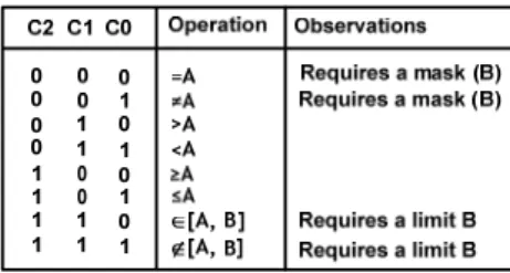
During the debug phase of an MS circuit its necessary to detect conditions in the analog and/or digital parts. The condition types accepted by the proposed circuit are listed and coded (C2,C1,C0) in Table 1. The MS condition detection mechanism reuses the IEEE1149.4 DBM (Digital Boundary Module, referred as BSC in the
IEEE1149.1 Std.) to build an elementary one bit comparator. In the Capture/Shift (C/S) stage is stored the limit B/mask bit while in the Update (U) stage is stored the limit A bit.
Table 1- Operation types performed by block F.
The bit value present at the Parallel Input (PI) will be compared against these limits in the combinational logic block F, as illustrated in Figure 2.
SI PI SO PO M D D M F PI C/S U DBM Q2,Q1,Q0 I2, I1, I0 C2,C1,C0 Q2,Q1,Q0 PI PO SO SI F I2, I1, I0 C2,C1,C0
Figure 2- The one bit comparator.
Depending of the selected condition type listed in Table 1, the update stage can be loaded with either a mask or a limit B. Each output block comparison (Q2,Q1,Q0) depends of the:
- actual bit to be compared (PI)
- A/B bit limits (stored on the C/S and U stages) - previous block F comparison result (I2,I1,I0) - selected operation type (C2,C1,C0)
The F result (Q2,Q1,Q0) corresponds to one of five possibilities: False, True, Equal to A, Great than A, or Less
than B; thus three lines (23) are needed to codify all these
possibilities. Table 2 presents, as an example, the truth table for the “=A” operation, i.e. (C2,C1,C0) = (0,0,0).
Table 2- Truth table of the one bit comparator for the “=A” operation.
1 1 1 T T X X X X X 0 U PI C/S 0 0 1 1 0 1 1 1 0 F T T F T T T T Coded I2,I1,I0 Q2,Q1,Q0Coded F F
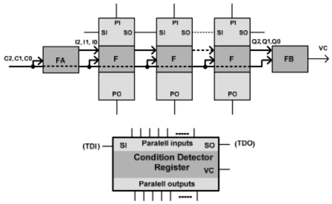
Several one bit comparators are cascaded to form the Condition Detector Register, as illustrated in Figure 3. This register works as a digital word comparator. The FA block, depicted in Figure 3, provides the initial condition values (I2,I1,I0) while the FB block decodes the last result (Q2,Q1,Q0) for the Valid Condition (VA) output. To detect conditions in both domains, two of these registers are needed: an Analog Condition Detector Register and a
Digital Condition Detector Register. The Digital Condition Detector Register is used directly in the digital nodes (input/output, pins/internal nodes as proposed in [3,4]) and may also be located in the analog/digital mission circuit interface, as recommended by the IEEE1149.4 Std.
Figure 3- The Analog and Digital Condition Detectors arrangement for MS circuits.
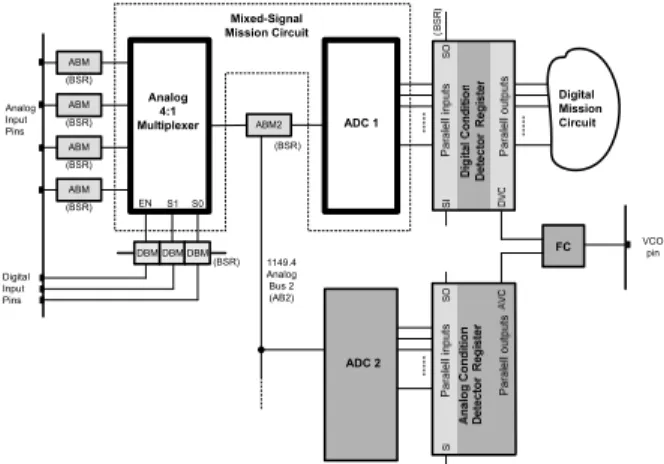
This recommendation is actually a rule when the device supports the INTEST instruction. The DBMs associated with the previously referred digital nodes are part of the Digital Condition Detector Register, and if the detection feature is not used, they will play their regular role within the BSR circuit. The Analog Condition Detector Register is a digital block, so an ADC is needed to convert the analog condition into a digital condition. The IEEE1149.4 infrastructure is reused to choose the node (analog/digital, pin/internal nodes) as proposed in [9]. Figure 4 illustrates the Analog and Digital Condition Detectors arrangement for MS circuits.
Figure 4- The Analog and Digital Condition Detectors arrangement for MS circuits.
The FC block presented in Figure 4 (right side) is responsible for selecting the signal that feeds the VCO pin, according to the conditions presented in Table 3.
Table 3- Truth table for the VCO pin value.
VS1 VS0 VCO pin DVC AVC DVC + AVC DVC * AVC 0 0 0 1 1 0 1 1 RTI state COMP2 0 X X X 0 X 0 X X 0 1 1 1 1 1 1 1 1
It allows to choose either the result of the analog or digital condition detection or a logic combination AND, OR of
both signals (this feature is founded in some trigger functionalities of mixed-signals oscilloscopes), by the VS0 and VS1 bits of the Detection Configuration Register. The FC block also impose that the VCO signal goes to logic high only when: (1) the Instruction Register (IR) is loaded with either instructions EXTEST2, PROBE2, or INTEST2 (described later in this paper); and (2) the TAP Controller is in the Run-Test/Idle state. The COMP2 signal listed in Table 3 is logic high when the IR is loaded with either instructions EXTEST2, PROBE2, or INTEST2. The operation type performed by each Analog/Digital Condition Detector Registers is selected, independently for the analog and digital parts, by the (C2,C1,C0) bits present in the Detection Configuration Register, as illustrated in Figure 5.
Figure 5- The Detection Configuration Register bits assignment.
The resulting register structure for an IEEE1149.4 compatible component is presented in Figure 6. The main differences are: the Analog Condition Detector Register, and the Detection Configuration Register. Notice that the Digital Condition Detector Register is based on the DBMs already present in the test infrastructure, which together with the TBIC and the ABMs control registers form the Boundary Scan Register (BSR).
Figure 6- IEEE 1149.4 register structure resulting from the present proposal.
The BSR is selected by the 1149.4 instructions EXTEST, SAMPLE/PRELOAD, PROBE, and INTEST. We propose a new and similar set of instructions that selects the BSR and the Analog Condition Detector Register (Figure 6 – data registers mux input 2): EXTEST2, SAMPLE/PRELOAD2, PROBE2, and INTEST2. In the remaining test infrastructure it is irrelevant to use the standard or the new proposed instructions. The SAMPLE/PRELOAD2 instruction is used to load the limit A value into the update stage of the Analog/Digital Condition Register. The EXTEST2, PROBE2, and INTEST2 instructions have similar functionality to the instructions defined in the standard with the difference that, when active, they cause the UpdateDR signal feeding the update stage to be disabled, in the Analog/Digital Condition Detector Registers. This allows the mask or limit B to be stored in the capture/shift stage, while not overwriting the information previously stored in the update stage (limit A). The new SELCON instruction places the Detection Configuration Register in the
TDI-TDO path, to allow the user to configure the conditions types and to select the signal for the VCO pin.
4. Verifying the condition detection
mechanism: a case study
The built-in condition detector has been simulated in the ORCAD environment. The complete MS circuit, presented in Figure 7, includes: (1) the target MS mission circuit; (2) the IEEE1149.4 infrastructure and its extension mechanisms to access internal nodes, as described in [9]; (3) and the proposed condition detector.
(BSR) ABM2 (BSR) ADC 1 Analog 4:1 Multiplexer Mixed-Signal Mission Circuit DBM DBM DBM ABM (BSR) ABM (BSR) ABM (BSR) ABM (BSR) EN S1 S0 Analog Input Pins ADC 2 FC VCO pin Digital Input Pins Digital Mission Circuit 1149.4 Analog Bus 2 (AB2)
Figure 7- MS circuit used for verifying the proposed built-in condition detector.
The target circuit consists of a 4:1 analog multiplexer and an ADC, named ADC1. The circuit exhibits the following characteristics:
- the digital input pins have DBMs - the analog input pins have ABMs
- the node situated between the analog multiplexer output and the ADC1 input there is an ABM2 compatible with the modules proposed in [9], which allows fully observability and controllability through the AB1/AB2 lines
- the digital nodes, located between the ADC1 outputs and the remaining digital mission circuit inputs, is placed the Digital Condition Detector Register instead of the recommended DBMs
- the Analog Condition Detector Circuit and the associated ADC, named ADC2, is part of the internal test infrastructure and is used to detect analog conditions
As an example, we now present the case where the “>A” and “<A” operations are used as the analog and digital detection condition respectively. For the analog part, the analog node under detection is the one that has the ABM2 associated with. The internal signal AVC must go high when the analog voltage present at that node is above the +6 V threshold. For the digital part, the internal signal DVC must go high when the digital word value (i.e. the ADC1 output in this case) is below a specific digital value, i.e. 011001101011, which corresponds voltage of -2 V being present at the ADC analog input. The VCO pin must go high when AVC or DVC exhibits a logic high. To select this operation, we first characterize the content
of the Detection Configuration Register, i.e. the (C2D,C1D,C0D), (C2A,C1A,C0A), and (VS1, VS0) values. For the first two sets we refer to Table 1 and for the third to Table 3. In the proposed example, for the digital detection operation we use “<A”, so the first set should be (C2D,C1D,C0D) = (0,1,1); for the analog detection operation we use “>A”, so the second set should be (C2A,C1A,C0A) = (0,1,0). The third set should be (VS1,VS0) = (1,0) since we want VCO to correspond to the logic OR operation between the AVD and DVC internal signals. The defined vector content (C2D,C1D,C0D,C2A,C1A,C0A,VS1,VS0) = (011’010’10) is shifted into the Detection Configuration Register using the SELCON instruction. Next, we have to select the analog limit A and the digital limit A. The first is obtained by converting the indicated analog value into the corresponding digital word (110011010101); the second is already a digital value (011001101011). These two values are shifted into the Analog Condition Detector Register using the SAMPLE/PRELOAD2 instruction. For the operations used (<A,>A) no limit B or mask is required, so we may shift all 1´s into the capture/shift stage of the analog/digital condition detector registers, using the PROBE2 instruction. The detection process starts in the moment that TAP controller enters the Run-Test/Idle state. While this instruction is active the detection process starts the moment the TAP controller enters the Run-Test/Idle state. The following paragraph illustrates, in pseudo-code, the steps required for configuring the 1149.4 test infrastructure with the described parameters.
Instruction Register ← SELCON;
%Select position 0 in the Data MUX (see Figure 6);
Detection Configuration Register (C2D,C1D,C0D, C2A,C1A,C0A,VS1,VS0)← 01101010;
%Shift the vector that selects the analog and %digital conditions types, and selects the analog OR %the digital detections to be outputted in the VCO %pin;
Instruction Register ← SAMPLE/PRELOAD2;
%Select position 2 in the Data MUX;
BSR + Analog Condition Detector Register ← (YYY 011001101011 11001101101);
%Shift the vector that selects the analog node %under %analysis (YYY) and the limit A for the Digital and %Analog Condition Detector Registers; the digital %value (that corresponds to -2V on the analog value) %is shifted into the Digital Part; the analog value %that corresponds to +6V is shifted into the Analog %part;
Instruction Register ← PROBE2;
%Select position 2 in the Data MUX;
BSR + Analog Condition Detector Register ← (YYY 111111111111 111111111111);
%Shift the vector that selects the analog node under %analysis (YYY) and the limit B for the Digital and %Analog Condition Detector Registers. Once the %selected operations (<A,>A) do not depends of %limitB/mask, all 1’s are shifted into Digital and %Analog Parts.
TAP controller ← Run/Test Idle;
The simulation process, done in the ORCAD environment, requires the designer to define the input signals, which on our circuit corresponds to the TAP input signals (TCK, TMS, and TDI). For this purpose we developed an in-house application, named BSOrcad, which automatically generates the TCK, TMS, and TDI signals. As input, this application accepts a test program written in a high level language, similar to Serial Vector Format [14]. As an output, BSOrcad
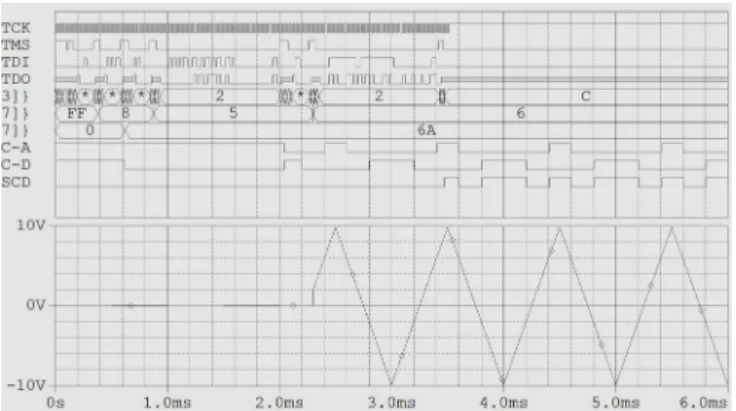
produces an <name>.stl file used directly by the ORCAD simulation tool. The Figure 8 exhibits the simulation results for the explained example.
Figure 8- VCO pin value for a sine wave present at AB2 - OR operation selected for AVC, DVC.
The following signals are displayed (by order of appearance):
- TCK, TMS, TDI, TDO - TAP controller coded state - Instruction Register content
- Detection Configuration Register content - Internal AVC signal
- Internal DVC signal - VCO output pin
- Analog signal present at AB2 (IEEE1149.4)
As expected, the VCO pin is logic high when the following occurs, simultaneously:
- the TAP controller is in Run/Test-Idle - instruction PROBE2 (06h) is active
- the analog voltage values in the selected analog node are above the pre-defined analog limit A (which corresponds to +6 V for the analog signal present in AB2) or the digital value is below the pre-defined digital limit A (011001101011)
From Figure 8 it is possible to observe that the TAP controller enters the Run/Test-Idle state, state coded as C hex, at 3.5 ms. Figure 9 shows the other MS detection situation, equal to the previous one on everything, except for (VS1,VS0) values, which are now (1,1), i.e. a logic AND between the AVC and DVC signals.
Figure 9- VCO pin value for a sine wave present at AB2 - AND operation selected for AVC, DVC
Signals AVC and DVC present the same values as in the previous example, while the VCO pin will go logic high when AVC and DVC are simultaneously at logic high. Provided that the circuit mission ADC is working properly it will be impossible to find situations where an analog signal is simultaneously above +6 V and below -2 V. This may however happen if instead of one analog signal we consider it and its conversion, coming from a block that may eventually fail. Therefore VCO is permanently at logic low, provided no errors occur, which may be seen as a possible debug scenario. These examples illustrate how the VCO pin may be used as a breakpoint signal, as earlier suggested in Figure 1. We presented an MS condition detection resulting from the observation of analog and digital values. On the proposed situation, used for illustrative purposes, a known correspondence exists between the analog and the digital values, since we are dealing with an ADC, as part of the MS circuit mission. However we must keep in mind that the MS circuit under debug can be much larger and the relation between the analog and the digital values can depend upon configurations, internal parameters, etc. This is the case, for instance, when the MS circuit contains a microprocessor that may output digital values (at its data bus), which are somehow related to an analog value present at a given MS circuit node.
5. Area penalties
The overhead is usually presented as a percentage of silicon area used by an extra-circuit. In this section, we consider the overhead introduced by the condition detection mechanism in relation to the mandatory 1149.4 test infrastructure. The IEEE1149.4 infrastructure complexity depends on two circuit groups: (1) a fixed one that includes the TAP controller, the IR, the Instruction Decoder, the TBIC switching and control structures, among other fixed blocks; and another one (2) that varies according the number of total nodes with ABMs or DBMs. For the overhead calculus we assume that:
- all digitals circuits are decomposed into elementary gates with two inputs (G2)
- all elementary gates with two inputs (G2) have similar complexity
The complexity on some blocks is block:
TAP controller N(G2) = 159
Bypass register N(G2) = 17
DBM N(G2) = 41
ABM (digital part) N(G2) = 165
where N(G2) represents the number of G2 gates expend in
each considered block. An 1149.1 test infrastructure has therefore a complexity of:
N(G2) = (556+41NDBM)
where NDBM represents the total number of DBMs in the
BSR. An 1149.4 test infrastructure comprehends a digital part, which can be expressed in a number of G2 gates, and a certain number of switches and comparators. Each of these three elements has an associated silicon area. In this paper
the circuit complexity is presented in simple terms of these elements, i.e. gates (G2 type), analog switches and comparators. An 1149.4 test infrastructure has therefore a complexity of:
N(G2, SWITCHES,COMPARATORS) =
(746+165 NABM+41 NDBM , 10+6NABM , 2+NABM )
where NABM represents the number of ABMs. An 1149.4
test infrastructure supporting the proposed MS condition detector circuit has therefore a complexity of:
N(G2, SWITCHES,COMPARATORS) =
(1091+165NABM+41NDBM+119NDREG+115NAREG ,
10+6NABM , 2+NABM )
where NDREG and NAREG represents the number of bits in
the Digital Condition Detector Register and Analog Condition Detector Register, respectively. Further, an
ADC with NAREG bits is added to the infrastructure. Table
4 presents the complexity associated to the different infrastructures.
Table 4- Infrastructure complexity.
# b its of t h e A D C ad ded # o f d igit al I/O # o f an alog I/O # o f equ iva len t C2 gat es # s w it ch es # c o mp arat ors # b its of th e d igita l regist er # bi ts o f th e an alo g re gis ter
These figures have been selected to allow a simple comparison. In the last case we assume that the Digital Condition Detector Register has replaced 8 existent DBMs. These examples permit to conclude that the condition detector circuit introduces a digital overhead of 33% in the 1149.4 infrastructure. For the MS part, one 8 bit-ADC must be added to the test infrastructure.
6. Conclusion
The work described in this paper addresses the problem of detecting mixed-signal conditions, as part of a debug operation. Many MS debug tools rely on physical access that is more and more compromised with the advances on miniaturization scales and operating frequencies. Therefore, new debug tools relying on electronic access are required for silicon diagnosis. Following this trend, the proposed built-in detector reuses the IEEE1149.4 test infrastructure to allow relating analog and digital values inside an MS circuit. The main limitation of the proposed mechanism is the overhead introduced in relation to the standard IEEE1149.4 infrastructure, which, however, is a small part of the global circuit size. If we consider an MS circuit with a microprocessor in its digital part, the total resulting overhead will be very low. The reduction in time-to-market, resulting from the benefits obtained
during the debug phase, may in fact justify the overhead costs associated to this solution. As future work we are evaluating the extension of the proposed circuit to improve the characterization of internal components.
References
[1] “The Rise of Digital/Mixed-Signal Semiconductors and Systems-on-a-Chip”, Cadence White Paper, 2002.
[2] IEEE Standard Test Access Port and Boundary-Scan Architecture, October 1993, IEEE Std. 1149.1, ISBN 1-55937-350-4.
[3] G. Alves, J. M. M. Ferreira “From for-Test to Design-for-debug-and-Test: Analysis of Requirements and Limitations for 1149.1”, Proceedings of the 17th IEEE VLSI
Test Symposium, 25-29 April 1999, pp. 473-480.
[4] G. Alves, J. M. M. Ferreira “Using the BS register for capturing and storing n-bit sequences in real-time”, Proceedings of the European Test Workshop, 25-28 May 1999, pp. 130-135
[5] K. Noguchi, M. Nagata, “On-Chip Multi-Channel Waveform Monitoring for Diagnostics of Mixed-Signal VLSI Circuits”, Proceedings of the Design, Automation and Test in Europe, 2004, pp 146-151.
[6] L Whetsel, “An IEEE1149.1 Based Logic/Signature Analyzer in a Chip , Proceedings of the International Test Conference, 1991, pp 869-878.
[7] IEEE Standard for a Mixed-Signal Test Bus, March 2000, IEEE Std. 1149.4, ISBN 0-7381-1755-2.
[8] M. Felgueiras, G. Alves, J. M. M. Ferreira “A Built-in Mixed-signal Block Observer (BIMBO)”, Proceedings of the 9th
IEEE European Test Symposium, 23-26 May 2004, pp 105-106.
[9] M. Felgueiras, G. Alves, J. M. M. Ferreira “Debugging mixed-signals circuits via the IEEE1149.4-analysis of limitations and requirements” Proceedings of the International Mixed-Signals Testing Workshop, 21-23 Jun 2006, pp 2-7. [10] U. Kac, F. Novak, F. Azais, P. Nouet, M. Renovell
“Extending IEEE1149.4 Analog Boundary Modules to Enhance Mixed-Signal Test”, IEEE Design & Test of Computers March-April 2003, pp 32-39.
[11] U. Kac, F. Novak, S. Macek, M.S. Zarik, “Alternative Test Methods Using 1149.4” Proceedings of the Design, Automation and Test in Europe, 27-30 March 2000, pp 463-467.
[12] P. Syri, J. Hakkinen, M. Moilanen, “IEEE1149.4 Compatible AMBs for Basic RF Measurements”, Proceedings of the Design, Automation and Test in Europe, 2005, pp 172-173. [13] M. Felgueiras, G. Alves, J. M. M. Ferreira, “A built-in
debugger for 1149.4 circuits”, Proceedings of the International Mixed-Signals Testing Workshop, 18-20 Jun 2006, pp 93-98.