• Nenhum resultado encontrado

Properties of coupled semiconductor quantum dot systems and their optical response

N/A
N/A
Protected

Academic year: 2019

Share "Properties of coupled semiconductor quantum dot systems and their optical response"

Copied!
175
0
0

Texto

(1)

CENTER OF EXACT SCIENCES AND TECHNOLOGY PROGRAM OF POST-GRADUATION IN PHYSICS

Properties of coupled semiconductor quantum dot

systems and their optical response

Luís Antônio Cabral

(2)

CENTER OF EXACT SCIENCES AND TECHNOLOGY PROGRAM OF POST-GRADUATION IN PHYSICS

Properties of coupled semiconductor quantum dot

systems and their optical response

Luís Antônio Cabral

Thesis presented to physics department of Federal University of São Carlos - DF/UFSCar as part of the

requirements for the PhD title in Physics.

Advisor: Prof. Dr. Victor Lopez Richard

Co-Advisor: Prof. Dr. Juarez Lopez Ferreira da Silva

(3)
(4)

During the period of development of this Thesis, I had the opportunity to interact with many people who contributed to this work. Thus, I will provide my special thanks.

Thanks to my advisor, Professor PhD Victor Lopez Richard, and co-advisor, Profes-sor PhD Juarez Lopes Ferreira da Silva, for the trust, availability and attention. There were several shared knowledges, solidifying and establishing the physical concepts in a simple and a productive way. All the support and infrastructure provided were fundamental for the results presented in this Thesis. Professors PhD Victor and Juarez had been present in every step, indicating the best way to obtain the results. In addition, they showed me the science in a elegant way.

In the same way, I’m grateful to Professor PhD Gilmar Eugenio Marques for the attention and encouragement, providing a productive environment for the development of the topics covered by this Thesis. To Professor PhD Matheus Paes Lima, whose teachings greatly contributed to the my scientific growth. To Professors PhD Leonardo Villegas Lelovsky and Anibal Thiago Bezerra for the valuable discussions in several physical systems that certainly favored my learning. To Professors PhD Adalberto Picinin and Luís Vicente Garcia for the motivation.

A special thanks to all members ofQuantum Theory of Nanomaterials, and Semi-conductors Nanostructuresgroups. In particular, to PhD Fernando Pereira Sabino, Professor PhD Vivaldo Lopes de Oliveira Neto and PhD Diego Guedes Sobrinho for the opportunity to work and collaborate. To PhD Diana Mercedes Meneses Gustin, Msc Carlos Mário Rivera Ruiz, Msc Carlos Maciel de Oliveira Bastos, Msc Rafael Costa Amaral and Felipe Antunes Calvi for friendship and companionship.

To my mother, Maria Antônia Cabral, for all teachings and support. And also,

(5)

To Professor PhD James Alves de Souza and Daniela Milani, whose solid friendship and reciprocity started as soon as we met at university and his daughter, Clara, whose sweet way rejoices our days filling with so much love and happiness. In the same way, to Ana, Danilo and their sons. To Patrícia Silveira Pinto, Patrícia Amanda Vieira, Janaína Martins Alves and Angélica Gasparotto for the solid friendship and for understand my absence along this research.

(6)

The study of doped semiconductor quantum dots with magnetic impurities has been a challenging task when adding spin-orbit coupling and exchange interaction with asymmetry effects. The combination of all these factors within a single theoretical model,

simultaneously analyzed with external fields, reveals interesting properties. Within this framework, the adjustment of the effective Zeeman splitting due to the asymmetry and the

character of the ground state are determined. The effective mass model of the electronic

structure, that allows combining different confinement profiles with reduction of controllable

symmetry, spin-orbit interaction effects and external fields under a variety of configurations,

in a systematic way has been complemented with atomistic simulations. The connection between the effective mass model and such atomistic approaches was done through a

charac-terization of the main trends for the manganese positioning (Mn) in cells containing cadmium selenide (CdSe) quantum dots covered by zinc selenide (ZnSe), as well as the exchange interaction terms, which is calculated with a fullyab initiotechnique.

Imperfections in nanostructures are also within the scope of this Thesis. Defects can induce magnetism in low-dimensional systems, wherein the challenge is to identify the source of this nano-magnetism in non-magnetic semiconductors, such as CdSe. In this Thesis, we present an optical evidence of this nano-magnetism due to the presence of vacancies. The formation energy analysis and the effects of the stress fields for the

charged and uncharged defects under various geometries provided a better understanding of the experimental results. In addition, a study of the local deformations was performed using the molybdenum disulfide (MoS2). Within the density functional theory, an organic

molecule, called azobenzene, was placed on the MoS2 layer in order to investigate the

adsorption properties of the system.

Key-words: k·peffective mass approximation, density functional theory, spin-orbit coupling,

asym-metry effects, quantum dots.

(7)

O estudo de pontos quânticos semicondutores dopados com impurezas magnéticas é uma tarefa desafiadora ao adicionar o acoplamento spin-órbita e a interação de troca com efeitos de assimetria. A combinação de todos esses fatores dentro de um único modelo teórico, analisado concomitantemente com campos externos, revelam propriedades interes-santes. Dentro desta estrutura, o ajuste do efeito Zeeman devido a assimetria e o caráter do estado fundamental são determinados. O modelo de massa efetiva da estrutura eletrônica, que permite combinar diferentes perfis de confinamento com redução de simetria controlável, efeitos da interação spin-órbita e campos externos sob uma variedade de configurações, de forma sistemática foram complementadas com simulações atomísticas. A conexão entre o modelo de massa efetiva e tais abordagens atomísticas foi realizada através da caracterização das principais tendências para o posicionamento do manganês (Mn) em células contendo pontos quânticos de seleneto de cádmio (CdSe) recobertos por seleneto de zinco (ZnSe), bem como os termos de troca, os quais são calculados com uma técnica completamenteab initio.

Imperfeições em nanoestruturas estão igualmente no escopo desta Tese. Defeitos podem induzir magnetismo em sistemas de baixa dimensão, em que o desafio consiste em identificar a fonte desse nano-magnetismo em semicondutores não-magnéticos, como o CdSe. Nesta Tese, apresentamos uma evidência óptica desse nano-magnetismo devido a presença de vacâncias. A análise das energias de formação e efeitos de campos de tensão para os defeitos carregados e não carregados em várias geometrias proporcionaram uma melhor compreensão dos resultados experimentais. Adicionalmente, um estudo de deformações locais no perfil de confinamento foi realizado utilizando o dissulfeto de molibdênio (MoS2).

Dentro da teoria funcional da densidade, uma molécula orgânica, chamada azobenzeno, foi disposta sobre uma camada de MoS2 para verificar as propriedades de adsorção do sistema.

Palavras-chave: aproximaçãok·p da massa efetiva, teoria funcional da densidade, acoplamento

spin-órbita, efeitos de assimetria, pontos quânticos.

(8)

1.1 2D materials. On the left, a bulk material composed by several 2D mono-layers. The in-plane bonds are covalent and the growth direction are related to the weak van der Waals forces. On the right, we represent the mechanical exfoliation technique. The 2D monolayer has been removed from the bulk material followed by the optical characterization, determining where the material will be deposited on the layer. . . 5

1.2 A layer of molybdenum disulfide (MoS2). Panel (a) indicates the single

MoS2 layer and panel (b) the monolayer multiplied by eight in the lateral

direction. . . 6

2.1 Crystal symmetry of solids. In panel (a) are depicted the Miller indexes and their respective planes. Panel (b) represents the cubic face centered unit cell for cadmium selenide bulk structure. Parts (c) and (d) show the primitive cell and the first Brillouin zone for the face centered cubic unit cell, respectively. 11

2.2 At the upper part of the Fig. the wavefunction expansion is depicted, where the slow and faster oscillation correspond to the envelope and the Bloch functions, respectively. At the bottom of the Fig. the potential that models the wavefunction is shown. . . 16

2.3 A schematic representation of the band structure for III-V semiconductors in the presence of spin-orbit interaction. The forbidden region E0, between the

conduction and valence bands, is also represented . The spin-orbit coupling introduces the energy gap,∆0, lifting the spin degeneracy between the heavy,

light holes, and the split-offsubbands. . . 18

(9)

sity is proposed. The effective potential is obtained to solve the Kohn-Sham

Eq. in order to determine the new wavefunctions and charge density. The cycle runs until the convergence of the charge density. . . 26

3.1 Quantum confinement profile. Panels (a) and (b) represent the confinement of quantum dot and ring, respectively. . . 45

3.2 Confinement potential profile in lateral direction fora2=4.47 meV/100nm2

and (a)δ1= 0 and severalδ2 values; (b)δ2= 0 and variousδ1 values. In (c)

and (d) panels are shown the ground state surface, whereδ2=−4 meV/100nm2

andδ2=12 meV/100nm2, repectively. . . 50

3.3 Fock-Darwin spectrum for CdSe QD under an applied magnetic field. The symmetric dispersion is represented by the dashed lines. The perturbative potential considers the eccentricity,δ1=1 meV/100nm2, and Gaussian

per-turbation, δ2=−4 meV/100nm2. In all calculations were fixed a1=0 and

a2=−4 meV/100nm2. . . 52

3.4 Interplay between wavefunctions in the indium arsenide (InAs) QD cov-ered by gallium arsenide doped with antimony (GaAs:Sb). In panel (a) a schematic representation of the experimental structure is shown. In panel (b) the distribution of the probability density of the holes ground state in the (110) and (110) planes is represented. In each panel the electric field intensity is indicated. . . 54

(10)

netic and electric field for a given confinement profile. In the panel (a) the effects of the confinement profile are indicated tuning the Zeeman splitting

and opening the possibility to control the spin character. The hybridization between the spin states is given in panel (b). By decreasing the electric field, the diamagnetic shift decreases, as indicated in panels (c) and (d). At the bottom of the Fig. the migration of the heavy holes states is depicted from the center to the edge of the QD due to the decrease of the electric field. . . 56

3.7 Effective Lande-factor including spin-orbit and asymmetry contributions in

units 2α/l20, described in Eq. (3.28). Panel (a) represent several values of∆/l0

without eccentricity perturbative potential forg(1)e f fg∗[2αs/l2

0] as function of

the angular amplitude of the defect,σ. In panel (b) are shown the calculated

values of theg(1)e f f g∗[2αs/l2

0] as function of the eccentricity withσ= ∆ =0. 60

3.8 Effective Lande-factor correction, in units ofΓ0 = 127kJ(0Tg+MnT

0)

a3 0

l2

0Lz, as function

of the asymmetric terms and magnetic impurity localized atϕ =π. In panel

(a) the effect of eccentricity is depicted, while in panel (b) the contribution

of a localized defect is represented. . . 61

3.9 Local density of states (LDOS) and band structure of the pristine cadmium selenide (CdSe) bulk system. In panels (a) and (b) the LDOS of the cadmium (Cd) and the selenium (Se) atoms are shown, respectively. Part (c) depicts the band structure of the CdSe, where the direct gap is indicated by theΓline. 62

3.10 Cadmium selenide (CdSe) quantum dot in zinc selenide (ZnSe) substrate doped with manganese (Mn). On the left, the density of states of Mn and CdMnSe/ZnSe QD are presented. On the right, the local density of states

(11)

Panel (a) represents the undoped QD, where the QD region is indicated by a circle. In panel (b) the Mn atom is shown replacing the zinc atom in the matrix surrounding the QD. The interstitial Mn doping sites are (c) in the center, (d) in the matrix and (e) in the edge of the QD. The substitutional Mn atom replaces the Cd atom in the configurations represented in (f-i) panels. . 65

3.12 Exchange interaction term (J0) and local density of states for bulk without

and with cadmium selenide QD doped by manganese. The CdSe QD is surrounded by ZnSe atoms. In panel (a) the calculatedJ0term is shown with

Hubbard correction for the bulk with and without QD. In panel (b) the local density of states is presented for CdMnSe bulk without QD usingUe f f = 0,

3 and 7 eV in p-Se and d-Mn states. In part (c) the local density of states is shown for CdMnSe bulk with QD in comparison to the bulk without QD usingUe f f =3 eV in d-Mn states. . . 67

3.13 Total density of states (DOS) of cadmium selenide bulk tensioned by 7.31 %.

The stress is equally introduced in the cartesian directions, compressing or enlarging the bulk. The DOS of the stressed structures is compared with the DOS of the same geometry without pressure. . . 69

4.1 (a) Transmission electron microscopy images (TEM) of two monolayers of the CdSe quantum dots. In panels (b) and (c) the micro-photoluminescence spectra is represented for three different quantum dots for several fields and

circular polarized detection. The unpolarized emission spectra were also added for certain fields values. Panel (d) depicts the peak emission positions of the quantum dot 2 (QD2) as function of the magnetic field strength forσ+ andσ−circular polarized emissions and part (e) details the Zeeman splitting

as function of the magnetic field. . . 75

4.2 (a) Time resolved integrated intensity measured at zero external field, B=0,

(12)

(CdSe) QDs embedded in a zinc selenide (ZnSe) host material with vacan-cies. Panel (a) the geometryCd-in:Cd vacancy inside the QD and isosurface 0.012eÅ−3. Panel (b) depicts the structure Cd-edge: Cd vacancy at the

edge of QD and isosurface 0.014eÅ−3. Panel (c) indicates the structure

Zn-matrix:Zn vacancy at the host material and isosurface 0.016eÅ−3. Panel

(d) represents the structureSe-in:Se vacancy inside the QD, which does not present magnetic moment. The QD region is depicted by a circle . . . 78

4.4 Formation energy for Cd-in, Cd-edge, Zn-matrix and Se-in structures, il-lustrated in Fig. 4.3. The calculations were performed for charged and un-charged states. The magnetic moment is indicated for each calculated structure. 80

4.5 Formation energy of charged and neutral geometries presented in Fig. 4.3 as function of the electronic chemical potential, where the structuresZn-in,

Se-in, Cd-edgeand Cd-indenotes the Zn vacancies in the matrix, Se inside the QD, Cd at the edge and inside the QD, respectively. . . 80

4.6 Formation energy and strain calculations. In panel (a) the QD atoms of the supercell are shown without defect and (b) the same QD region with defect, representing theCd-ingeometry. The atomic displacements are indicated by blue arrows. In panel (c), the strain is calculated as function of the formation energy, where strain effects are due to the lattice parameter variation. Panel

(d) shows a comparison between the Cd-in and Se-in chemical potentials. . 81

5.1 Azobenzene isomerization by light incidence with energy ~ν. In the left

(right), the trans- (cis-) configuration is depicted. . . 84

5.2 Azobenzene in gas-phase. In panels (a) and (b) the trans- and cis-configurations are depicted, respectively. The angles and Bader charge transfer between the atoms are indicated in the Figure. The angles between the carbon and nitrogen atoms for the cis- and trans- isomer are 123◦and 115, respectively.

The effective Bader charge on the nitrogen atoms for the cis- and

(13)

top of the Fig. are shown the LDOS of the cis- isomer and, at the bottom, are presented the LDOS of the trans-azobenzene configuration. . . 88

5.4 Molybdenum disulfide (MoS2) band structure and local density of states. At

the top (bottom) the bulk (layer) is represented. On the left (right) the band structure (local density of states) is depicted. At the upper part of each band structure, the points of the Brillouin zone are shown. The MoS2bulk (layer) presents an indirect (direct) gap energy. . . 89

5.5 Adsorption of the azobenzene molecule on the molybdenum disulfide (MoS2(0001))

layer. In the Figure are depicted the side and top views of the calculated geometries. . . 91

5.6 Top and side views of the lowest energy configurations, TransHd and CisHd. In the top view the effective Bader charge is indicated and, in the side view,

the vertical distance between the surface and the closest atom of the molecule is shown. The electron density differences induced by the azobenzene on the

surface are depicted at the bottom of the Figure. . . 93

5.7 Azobenzene molecule at the top of one (a) and three (b) MoS2(0001) layers.

To understand the role of the layer in the electronic properties of the azoben-zene, the number of layers was increased of the lowest energy configuration, TransHd. . . 95

5.8 Local density of states of the trans-azobenzene on the molybdenum disulfide surface. On the left (right) the trans-azobenzene placed at the top of one (three) MoS2(0001) layers is depicted. . . 96

5.9 Bader charge analysis for cis- (a,c) and trans- (b,d) azobenzene isomers placed at the top of one (a,b) and three (c,d) MoS2(0001) layers. Here

(14)

lic contacts are placed (a) on the layered 2D dichalcogenide (TMD), (b) lat-erally linked at the edge of the TMD and (c) combined with the dichalcogen layers. . . 101

D.1 Local density of states as function of the effective Hubbard Ue f f correction

ondcadmium and zinc states in CdSe and ZnSe pristine bulk structures. . . 118

D.2 Comparison between the CdSe bulk doped by Mn and the CdSe QD doped by Mn within the ZnSe substrate for the exchange interaction parameter as function of the DFT total energy and the effective Hubbard correction. At

upper part of the Fig. we represent the bulk without QD and, at the bottom, the bulk with QD. In both cases, the Mn impurity replaces one Cd atom. . . 123

D.3 Exchange interaction parameter for the geometries with and without CdSe QD. The distinct behavior of the exchange interaction is due to the QD presence in the bulk, introducing a strain and changing the local environment of the structure. . . 124

E.1 Calculated values for the lattice parameter, gap energy, and total energy for several k-density values using PBE exchange and correlation functional. The special grid of 25 k-density provides a good accuracy of the obtained results, which corresponds to ak-mesh of 4x4x4. . . 129

E.2 Lattice parameter of cadmium, selenium, and zinc in hexagonal close pack-ing bulk structures analyzed as function of the k-density samplpack-ing. These obtained results were used in the calculation of the chemical potential of the chapter 4. The properties achieve the accuracy for 30 k-density. . . 130

E.3 Molybdenum disulfide (MoS2) lattice parameters as function of thek-points.

The convergence tests were performed using bulk structures in Octahedral geometry, where the 25 k-density gives the converged values for the MoS2

lattice parameters. The calculated lattice parameters and the k-mesh were

(15)

4.1 Calculated values for the geometries presented in the Fig. 4.3. qC, Mag. Mom and EFor are the charge, magnetic moment and formation energy,

re-spectively. . . 79

5.1 Adsorption of the azobenzene molecule on the single MoS2(0001) layer:

distance between the azobenzene and the layer (dF), adsorption energy (Ead),

work function (Φ) and the total energy difference (∆En) between the smallest

configuration energy and the considered geometry. . . 92

D.1 Effective Hubbard correction Ue f f on d states of cadmium and zinc atoms

applied to obtain a better accuracy of the lattice parameter (a0) and gap

energy (Eg) of the pristine CdSe and ZnSe bulk structures. . . 118

D.2 Calculated values of the lattice parameter (a0) and gap energy (Eg) with and

without Hubbard correction Ue f f=7.0 eV ond-Cd andd-Zn states for CdSe

QDs within ZnSe host material. . . 119

D.3 Effective coordination number (ECNatom) and average distance (datomAV ), where

atom is the chemical specie (Mn, Cd, Se, Zn), with and without Hubbard correction. . . 119

D.4 Local magnetic moment (Local Mag.) and final magnetic moment (Final Mag.) of the CdSe QDs undoped and doped by Mn impurity in ZnSe sub-strate. The calculations were performed with and without Hubbard correc-tion ofUe f f =7.0 eV ond-Cd andd-Zn states. . . 120

D.5 Calculated values for the exchange interaction parameter for the cadmium selenide bulk doped by manganese impurity. . . 121

(16)
(17)

QW Quantum Well

QD Quantum Dot

QR Quantum Ring

HH Heavy Hole

LH Light Hole

DFT Density Functional Theory

ZB Zinc Blend

WT Wurtzite

RS Rock Salt

SOC Spin-Orbit Coupling

FD Fock-Darwin

DMS Diluted Magnetic Semiconductors

DOS Density of States

LDOS Local Density of States

VASP Vienaab initioSimulation Package

FM Ferromagnetic

AFM Anti-Ferromagnetic

ECN Effective Coordination Number

VBM Valence Band Maximum

CBM Conduction Band Minimum

MBE Molecular Beam Epitaxy

TMD Transition Metal Dichalcogenides

BOAP Born-Oppenheimer Approximation

HK Hohenberg-Kohn

KS Kohn-Sham

MBP Many Body Problem

LDA Local Density Approximation

LSDA Local Spin Density Approximation

GGA Generalized Gradient Approximation

(18)

BJ Becke Johnson

PBC Periodic Boundary Conditions

AE All Electron

PAW Projector Augmentation Waves

OPW Orthogonalized Plane Waves

APW Augmented Plane Waves

PS Pseudopotential

QCSE Quantum Confined Stark Effect

PL Photoluminescence

TEM Transmission Electron Microscopy Images

(19)

1 Introduction and motivation . . . 1

1.1 Manganese, cadmium selenide and indium arsenide . . . 4

1.2 Transition metal dichalcogenides . . . 5

1.3 Thesis scope . . . 7

2 Backgrounds for the electronic structure simulations . . . 9

2.1 Crystal symmetry and properties of solids . . . 10

2.1.1 Lattice and unit cells of crystal structure . . . 10

2.2 k·pmethod . . . 12

2.2.1 k·pHamiltonian . . . 12

2.2.2 Effective mass approximation . . . 15

2.2.3 Envelope function approach . . . 16

2.2.4 The Kane Approximation and Luttinger Hamiltonian . . . 17

2.3 Density functional theory . . . 19

2.3.1 The many body problem . . . 19

2.3.1.1 Born-Oppenheimer approximation . . . 20

2.3.2 Density functional theory . . . 21

2.3.2.1 Hohenberg-Kohn theory . . . 22

2.3.2.2 Kohn-Sham theory . . . 23

(20)

2.3.3 Exchange and correlation functionals . . . 27

2.3.3.1 Local density approximation . . . 27

2.3.3.2 Generalized gradient approximation . . . 28

2.3.3.3 On site Coulomb interaction: L(S)DA+U . . . 31

2.3.3.4 van der Waals corrections . . . 33

2.3.4 Monopole, dipole and quadrupole correction in solids . . . 35

2.3.5 Computational approach . . . 36

2.3.5.1 Planes waves . . . 37

2.3.5.2 The projector augmentation waves method . . . 39

3 Quantum wells, rings and dots . . . 42

3.1 Quantum well . . . 43

3.2 Quantum dot and ring confinement . . . 44

3.3 Spin-orbit interaction in quantum dots . . . 44

3.3.1 Fock-Darwin spectrum . . . 45

3.3.1.1 Case:ω0>> ωc . . . 48

3.3.1.2 Case:ωc >> ω0 . . . 48

3.3.2 Asymmetry effects in quantum dots . . . 48

3.3.3 Rashba spin-orbit in CdSe quantum dots . . . 50

3.4 Quantum dot and ring under electric field . . . 52

3.4.1 Stark effect and quantum confined Stark effect . . . 53

3.4.2 Electric and magnetic field in valence band states . . . 53

3.4.3 Effective Lande-factor and exchange interaction in CdSe quantum dots 57

(21)

3.6.1 Stress tensor effects . . . 68

3.6.2 Effective coordination number concept . . . 68

4 Calculations for vacancies in solids . . . 71

4.1 Energy of formation . . . 72

4.2 Defect induced magnetism in CdSe QDs . . . 73

4.2.1 Cadmium selenide in zinc selenide host material: a density func-tional theory investigation . . . 76

5 Adsorption properties of organic molecules on 2D semiconductor layers . . . 83

5.1 Atomic configurations: azobenzene . . . 85

5.2 Azobenzene in gas-phase . . . 85

5.3 Bulk and layered MoS2systems . . . 87

5.4 Azobenzene on the MoS2layer . . . 90

5.5 Azobenzene adsorption on MoS2(0001) . . . 92

5.6 Work function . . . 94

5.7 Density of states . . . 94

5.8 Charge transfer analaysis - Bader . . . 95

6 Conclusions and future perspectives . . . 98

A Spin-orbit interaction calculations . . . 102

A.1 Growth direction . . . 102

A.1.1 Conduction band - electrons . . . 102

A.1.2 Valence band - heavy holes . . . 105

(22)

A.2.1.1 Gaussian perturbative potential . . . 110

B Bump size in the potential profile . . . 113

C Luttinger model . . . 114

D Exchange interaction parameter . . . 117

D.1 Cadmium selenide and zinc selenide in bulk model - GGA+Ue f f . . . 117

D.2 CdSe and ZnSe quantum dots . . . 118

D.3 Exchange interaction calculation . . . 120

D.3.1 Bulk without quantum dot . . . 121

D.3.2 Bulk with quantum dot . . . 121

D.3.3 Comparative results . . . 122

E Theoretical approach and computational details . . . 125

E.1 Convergence tests . . . 127

(23)

Introduction and motivation

Several problems in semiconductors physics are analyzed within the framework of quantum mechanics. A better understanding of the confinement profile is crucial to determine the electronic properties of the system. In turn, solid state physics gained notoriety with the extension of bulk crystals theories for the investigation of thin films and multi-layered systems. Advances in Molecular Beam Epitaxy (MBE) [1] allowed the growth of individual atomic monolayers, [2] whose properties are mainly determined during the synthesis process. The orientation of the substrate where the nanostructures will be grown and the anisotropic effects that favor certain directions are responsible for the determination

of the electronic structure of these semiconductor systems. This experimental control of heterostructures growth also provides fundamental technological advances. [3] Modern techniques allow the manipulation and creation of notable confined systems. Thus, in the last 20 years, a breakthrough in the studies of nanostructured materials has taken place.

Advances have been made in the study and applications of electrons confined in two dimensions, in particular, the quantum wells (QWs). The QWs are nanostructures that can be formed by stacking semiconductor layers. Thus, the simulation of their electronic structure reveals quantization effects as described by quantum mechanics. After the discovery of

two-dimensional systems, there was an intense quest for the study of their properties and applications. The result, for instance, was the emergence of pioneering theories such as the Quantum Hall Effect [4] by Klaus von Klitzing’s, winning work of the Nobel Prize in 1985,

followed by the Fractional Quantum Hall Effect [5] by H. L. Tsuiet al. and the theoretical

works of Laughlin. [6–8]

(24)

In the early 1980’s, the progress in growth and lithographic techniques allowed the study of the electronic confinement of almost-one dimensional structures, called quantum wires. [9] Subsequently, the quantization of the electrons in quasi-zero dimensional struc-tures provided the emergence of quantum dots (QDs), firstly synthesized by scientists from Texas Instruments Incorporated. Reedet at reports the quantum dot growth by lithography techniques. [10] Afterward, research centers such as AT & AT Bell Laboratories [11, 12] and Bell Communication [13] reported the creation of quantum dots with diameters between 30-45 nm.

Quantum dots [14] are semiconductor nanostructures of dimensions as small as 10−8 and 10−6m [15] whose controllable properties allow several theoretical studies and

experimental manipulations. The description of quantum mechanics is used to analyze the properties of electrons and holes confined in the three spatial dimensions within the quantum dots. Due to this characteristic, quantum dots are usually known as almost-zero dimensional structures. This three dimensional confinement provides the quantization of the quantum dots states in discrete energy levels similar to an atom. [16] Optical transitions are thus allowed between these levels according to the selection rules for photon emission and absorption. Thus, the optical and electronic properties are directly and indirectly detectable from the light interaction. [2, 17]

Although the quantum dots are called as artificial atoms, there are considerable differences between an artificial and a natural atom. Concerning the electronic structure

of quantum dots, the separation between energy levels can be in the order of meV and the external control of the confinement potential can be attained, while in natural atoms, the separation of energy levels is in the order of eV.

The possibility to modify the geometry of confinement and the carrier dynamics through the application of external electromagnetic fields opens a wide range of studies. It is possible, for instance, to analyze the behavior of one or more particles bound in a parabolic potential induced by a magnetic field, the quantization of Landau levels, the ra-diative recombination of carriers, and so on. Among several theoretical frameworks, the

k·pFock-Darwin description of confined carriers in quantum dots under the influence of an

(25)

methods. Both treatments,k·pandab initiosimulations are combined within this Thesis.

In addition, it is interesting to note that QDs can be structurally coupled, as in the case of self-organized systems or optically coupled via light interaction. The flexibility of manipulating the energy levels through the incidence of electromagnetic fields makes the QDs attractive to the scientific community, providing advances in the segments of optical detectors, transport, Rabi oscillations, decoherence, and quantum computing. An interesting study of the QDs dynamics asqubitswas done by Loss and Divicenzo. [18]

Currently, several QDs growth processes are available that control their shape and radius. The control of the QDs geometry depends on the pressure and temperature during the growth process: chemical techniques, [19] lithographic, and MBE or MOCVD (Metal-Organic Chemical Vapor Deposition). Self-assembled QDs, grown by MBE and MOCVD, attracted the attention of the scientific community for applications in electronic semiconduc-tor devices, such as the buildup of high temperature lasers and quantum computing schemes, wherein different lattice parameters of deposited materials lead to unavoidable strain fields

and the possibility to form electron traps.

With the advent of the spintronics, the efforts for the manipulation of spins in

semiconductor nanostructures became evident in several areas including Condensed Mat-ter and Quantum Information. The first proposal for spin manipulation in nanostructures was introduced by Datta-Das, [20] wherein the authors explore the effects of the spin-orbit

interaction in a 2D gas in order to manipulate and detect the polarized spins. In this way, spin and charge carry information. The spin control is particularly interesting for the construction of quantum computing devices because its operation is based in a coherent superposition of quantum states of two-electronic levels. [18] The understanding of the mechanisms that destroy the states superposition becomes crucial for modeling this systems. [21] The spin-orbit coupling is a potential source of spins relaxation, allowing the mixing of spins states. [22, 23] Thus, the combination of spin-effects, geometry, and strain is a topic of

(26)

1.1

Manganese, cadmium selenide and indium arsenide

Cadmium selenide (CdSe) is a II-VI semiconductor material. The most stable phases are zinc blend (ZB), wurtzite (WT), and rock salt (RS). [24] The experimental lattice parameter in zinc blend phase assumes 6.05 Å and the bulk modulus 53.0 GPa. CdSe shows

a direct band gap in the gamma point, namely, 1.90 eV. [25] By growing the CdSe QD

on another substrate material, an unavoidable strain occurs due to the lattice parameters difference. In this Thesis, we analyzed the CdSe QDs grown on zinc selenide (ZnSe)

substrates. Zinc selenide crystallizes in zinc blend phase with 5.67 Å and 2.82 eV of lattice

constant and gap energy, [24, 26, 27] respectively. In turn, indium arsenide (InAs) is a III-V semiconductor widely employed in nanoelectronic devices based on quantum well structures. [28] The stable phase of the bulk InAs is the zinc blend, having a cubic lattice parameter of 6.06 Å length and a narrow band gap of 0.42 eV, [29] with a strong non-parabolicity of the

conduction band. In this work, we studied the InAs QDs within gallium arsenide doped with antimony (GaAs:Sb).

The formation of semiconductor QDs inside the host materials induces strain, com-pressing the bond lengths and introducing some perturbations in the chemical environment of the solid. Setting the CdSe QDs diameter between 2.0-7.0 nm leads to the emission

between 450-650 nm. [30] Changing the composition to CdSe1−xTe1−x and radius 5.0 nm,

the emission appears between 610-800 nm. Thus, the notoriety for the particular case of CdSe QDs is the photo-stability, wherein the composition plays a key role. Usually, CdSe QDs passivated with zinc sulfide (ZnS) [31] have been used in medical [32] and biological [33] applications, preserving the core from oxidation and also promoting an increase in the photoluminescence. Usually, the InAs QDs are grown on gallium arsenide. [34] The charac-terization of the atom-like energy levels of InAs QDs are presented, for instance, in Ref. [35]. Within the effective mass theory, strain effects in InAs QDs were studied in Ref. [36]. These

(27)

1.2

Transition metal dichalcogenides

The transition metal dichalcogenides (TMD) are composed by a transition metal and a chalcogen atom, such as molybdenum and sulfur, respectively. The transition atoms in the layer are strongly bonded while the atoms between the layers are linked by van der Waals (vdW) forces. [37] Due to layers formation, it is possible to exfoliate the bulk in thin layers and study them individually. Commonly, each layer is composed by three atomic planes with thickness around 6.0-7.0 Å. Furthermore, the structure of the TMD is

composed by hexagonal layers. In general, the TMD material crystallizes in the hexagonal (2H) (P63/mmc), trigonal (1T) (P3m1) [38] and rhombohedric (3R) (R3m) forms1, [39]

wherein the most of TMDs prefer 2H geometry.

The TMD are intensely studied due to the wide range of applications and the possi-bility to constitute layered materials, used in several areas. [40–43] In addition, TMD attracts the attention due to its applications in 2D nano-devices. [44] First-principles calculations based on the density functional theory can foresee new materials and their electronic and chemical properties. The pioneer 2D material obtained was graphene, attracting attention of the solid-state community due to the interesting electronic, optical, thermal, and mechanical properties. [45] Moreover, graphene is still explored in several studies. [46] The intensive study of graphene increased the interest in others two-dimensional materials. From that point, new 2D materials have been exfoliated from their bulk structures.

Figure 1.1: 2D materials. On the left, a bulk material composed by several 2D monolayers. The in-plane bonds are covalent and the growth direction are related to the weak van der Waals forces. On the right, we represent the mechanical exfoliation technique. The 2D monolayer has been removed from the bulk material followed by the optical characterization, determining where the material will be deposited on the layer.

(28)

In Fig. 1.1, taken from Ref. [47], we represent a bulk formed by several monolayers in the left and the mechanical exfoliation process in the right. The exfoliation is performed together with the optical characterization to determine where the material will be deposited on the substrate. However, the time used to produce the new layers is the major disadvantage. As mentioned above, the gap values of the TMD semiconductors can be tuned according to the experiment. By applying external voltages, by inserting or removing the number of layers, it is possible adjust the gap, which changes the confinement profile and, consequently, modifies the optical and electronic properties of these solids. Moreover, some 2D materials, such as HFSe2 and HF2, have considerable mobilities of carriers and electron masses along

Γ-M direction. [47] However, several band structures parameters, such as effective masses

and carrier mobility, are not available in the literature. Thus, the density functional theory is used in order to determine these values with high accuracy. The spin-orbit coupling in TMD is strong due to d-orbitals of metal ions. The inversion symmetry in bilayer of MoS2can be

controlled by applying an electric field perpendicular to the layer. [38]

Molybdenum disulfide (MoS2) has been widely used in several areas of research, such as photoelectrochemistry [48] and photovoltaics [49], due to its electronic, optical [50] and catalyst properties. Single MoS2 layers have been explored due to their potential

applications in electronics and nano-devices. [51] MoS2 bulk semiconductor shows an

indirect gap of 1.2 eV, however the monolayer presents a direct forbidden region of 1.8 eV.

[38] Molybdenum disulfide belongs to the P63/mmc space group. [47] The hexagonal lattices

constants area=3.16 andc=12.58 Å. [38, 52] The gap modulation by the number of layers

allows foreseen their use for phototransistor architectures. [53]

Figure 1.2: A layer of molybdenum disulfide (MoS2). Panel (a) indicates the single MoS2layer and panel (b)

the monolayer multiplied by eight in the lateral direction.

The emergence of new technological devices has been the topics of research of several groups. [46] Dolui group shows that the MoS2 conductivity depends on the charge

(29)

when the MoS2 is deposited on the SiO2 substrates. [55, 56] The effect of substrates on

the electronic properties of these 2D systems is a current investigation trend. A wide range of possibilities can be opened by varying the chemical environment and by the potential functionalization of the surfaces, as discussed in this Thesis.

1.3

Thesis scope

The main object of this Thesis is to tackled problems related to the properties of confined semiconductors systems. For this, in chapter 2, we present the methodological backgrounds of the electronic structure characterization that provide the bases for the theo-retical investigations. In particular, the general aspects of the crystal symmetry and properties of solids are presented in chapter 2. After that, thek·pmethod is discussed to describe the

electronic structure of semiconductors. The atomistic effects are analyzed within the density

functional theory. Here, the Projector Augmentation Waves (PAW) method was used, as implemented in the Vienaab initioSimulation Package (VASP).

One of the questions to be answered in this Thesis concerns the spin modulation with geometry, strain, and impurities, all combined within the same framework. In general, these effects are tackled separately so that their relative importance can seldom be weighted.

We are able to describe how they impact the spin ground state under the influence of a magnetic field. The results of the electronic structure calculations for CdSe quantum dots and InAs rings are shown in chapter 3. The shape and the quantum confinement are emulated through a variable potential. A more realistic implementation of the theoretical model is given by the external asymmetries and the spin-orbit coupling. In addition, the introduction of magnetic impurities allows to study the exchange interaction coupling between the s-p

states of the host material andd levels of the impurity. The exchange interaction coupling was also investigated at atomistic scales using first principles calculations within the density functional theory framework, wherein a manganese (Mn) atom enters replacing the cadmium and zinc atoms in cadmium selenide (CdSe) quantum dots embedded in a zinc selenide (ZnSe) host material. Interstitial manganese atoms inside the crystal were also implemented to contrast various configurations. The interplay between the results of thek·pmethod and

(30)

Several imperfections can also occur in the growth process of the semiconductor nanostructures. In general, the presence of the imperfections in the crystalline structure distorts the electronic structure of the materials, providing new effects. The defects can

be reproduced by the introduction of magnetic impurities, interstitial atoms and, the most common, vacancies. Thus, taking advantage of the first-principles calculations, the aim of chapter 4 is to provide the theoretical bases to explain the magnetism induced by vacancies in CdSe quantum dots embedded in ZnSe host material observed in the experiments. For this, several vacancies positions of Cd, Se and Zn atoms were created for the analysis of the magnetic moment and formation energy.

Based on experimental motivations, in chapter 5 we show the results of the ad-sorption of organic azobenzene molecules on the surface of molybdenum disulfide (MoS2). Using the density functional theory, the azobenzene molecule was studied in its cis and trans isomers in gas phase. Concomitantly, the electronic properties of MoS2 were also explored, showing the band gap transition from indirect (bulk) to direct (layer). The understanding of the quantum confinement within MoS2 plays a key role to study the electronic states of the azobenzene on the layer. Thus, various configurations of the azobenzene molecule were placed on the MoS2 layer, where the adsorption properties, the work function, the charge

transfer, and the stability of the configurations were analyzed and contrasted to determine the most stable and energetically favorable structure.

(31)

Backgrounds for the electronic structure

simulations

The three-dimensional periodic arrangement of crystals simplifies the theoretical description of the materials, allowing to link the real experiment and data analysis. There is a wide range of structures formed by different combinations of atomic species, wherein

the introduction of the external forces, pressure and fields can result in distortions in the crystal. The intense search for the construction of electronic nano-devices, has promoted the evolution of techniques to study and simulate solids. In our case, thek·pmethod and density

functional theory (DFT), or the interplay between them, were used to describe the electronic systems analyzed in this Thesis.

Both methods, k·p and DFT, are within the scope of many-particle physics. The k·pmethod is used to determine the details of the band structure in the neighborhood of an

arbitraryk0point. The consistency and flexibility allow to emulate the optical and electronic

properties of solids. The parameters used in thek·ptheory are obtained from experimental

techniques orab initiocalculations. [57] On the other hand, the density functional theory is used for investigations at atomistic scales using first principles methods. Here, mechanisms to address the electronic structure of systems of interest were introduced by complementing methodologies. So, when necessary, both DFT and k·p, will be used for modeling the

problems tackled in this work. These tools are essential to understand the matters discussed in this Thesis. Thus, in the following subsections we present the theoretical foundations that support the obtained results, discussed in the following chapters of this Thesis.

(32)

2.1

Crystal symmetry and properties of solids

The periodic arrangement of atoms in the lattice defines a crystal. Due to the technological applications, [3] the crystalline materials are widely studied. The crystals are described by their symmetry operations. The translations group and point operations, such as rotations, reflections and inversions, define the space group of the crystal. The non-crystalline materials receive a separate treatment because their atoms are randomly dis-tributed. Unavoidable imperfections during the crystal growth, such as vacancies, impurities, and extra interstitial atoms can determine new effects in the optical and electronic properties

of the crystal. In the next sections, we present the crystal properties and this theory will permeate all this Thesis.

2.1.1

Lattice and unit cells of crystal structure

The advancement of the theoretical descriptions allows to emulate the electronic structure of real experiments and foresee new optical and electronic properties of bulk crys-tals. The periodic arrangement in crystalline solids are described by the Lattice Bravais

concept, wherein the position R is specified as a function of the primitive lattice vectors

ai, i = 1,2,3, given by the relation R = n1a1 + n2a2 + n3a3, wherein n1, n2 and n3 are

integers. Therefore, the crystal lattice is described by the primitive vectors. Theprimitive cellis a cell with a minimum volume and, when translated by theBravaisvectors, occupies the whole space and its vectors are calledprimitive basis vectors. A unit cell is larger than the primitive one, which can be translated and fill the space region, reproducing a similar region of the crystal. [2] The lattice parameters are the vectors which describes the unit cell. The periodic arrangement of the crystal defines the reciprocal lattice.

Due to the diversity of crystal lattices, it is appropriate to analyze the symmetry of the unit cell. The point symmetry determines fourteen different lattices and the cells are

(33)

normal to that plane.

Figure 2.1: Crystal symmetry of solids. In panel (a) are depicted the Miller indexes and their respective planes. Panel (b) represents the cubic face centered unit cell for cadmium selenide bulk structure. Parts (c) and (d) show the primitive cell and the first Brillouin zone for the face centered cubic unit cell, respectively.

The III-V nanoscopic systems crystallize in zinc blend (ZB) structure. The ZB phase consists in two interpenetrating face centered cubic lattices placed at a

4 along the main

diagonal of the cube, whereinais the lattice vector. The ZB is not a Bravais lattice due to its atomic composition. The first Brillouin zone of the reciprocal lattice is a truncated octa-hedron, wherein the top of the valence band occurs at theΓ-point. [59] The crystallization

(34)

The space lattice of the WT is composed by a hexagonal structure in four interpenetrating lattices, [60] wherein the basisa1 anda2 are two identical atoms associated to each point of

the lattice and thea3axis is perpendicular to them. [58]

2.2

k

·

p method

Within the many body problem, a consistent analysis of the electronic and optical properties of solids can be performed using thek·p method. [61–68] Taking advantage of

the lattice periodicity, the method allows to determine an effective Hamiltonian of the system

within the mean field approach. The wavefunction is expanded in terms of the k vectors.

Thus, thek·papproach is a consistent mathematical tool for the investigation of the electronic

stracture in a neighborhood of an arbitrary point, and the validity of the method is restricted to this neighborhood. In fact, thek·papproach is based in the determination of the Hamiltonian

in a representation which couples the energy states in the k=k0 point in order to solve the

eigenvalue equation, introducing the appropriate approximations. In this Thesis, we used the parabolic approximation for the conduction band and the Luttinger model for the valence band. Due to the versatility and relatively simple mathematical manipulation, thek·pmethod

is widely used in the study of the band structure of materials. In addition, the Brillouin zone is fully described by increasing the number of wavefunctions. The diagonalization of the effective Hamiltonian chosen at k point must provide the energy states. A complete

description of solids is conditioned by a previous determination of material parameters, which is given by experimental data or first principles calculations.

2.2.1

k

·

p Hamiltonian

The mathematical modeling of a solid must include all the interactions between electrons and nuclei. Each carrier is subjected to the interaction with other carriers in the lattice under an effective potential. Thus, the strategy adopted is to assume a charged carrier

moving in a crystal lattice under the influence of the mean field due to the periodic potential

U(r+R) = U(R), whereinris a vector of theBravaislattice. The eigenvalues is obtained

(35)

H0Ψk(r)= εΨk(r), (2.1)

where H0 = p

2

2m0 +U(r), with p=−i~∇is the linear momentum operator and m0 is the free

electron mass. Due to the crystal periodicity, the eigenstates of the wavefunction can be expanded according to the Bloch theorem: [2]

Ψnk=eik·runk(r), (2.2)

whereunk(r) is the Bloch wavefunction,kthe wave vector andnthe band index. Expanding

the operatorH(k)=e−ik·rH0eik·rin Taylor series,

H(k)= H0ik·[r,H0]− 12

X

i j

kikj[ri,[rj,H0]]+. . . , (2.3)

where the commutators are [r,H0]=im~0p and [ri,[rj,H0]]=−i~

2

m0δi j, neglecting the higher

order terms. Replacing the anti-commutators in Eq. (2.3), the result is:

H(k)= p 2

2m0

+U(r)+ ~k 2

2m0 + ~

m0

k·p. (2.4)

By using the Bloch theorem, it is interesting to rewrite (2.4) in the following way:

"

H(k0)+

~k2

2m0 + ~

m0

k·p

#

unk(r)= ε(k)unk(r). (2.5)

Expanding the Bloch functionsunkin terms of theun′k0 in thek=k0, unk(r)=

X

n′

cnn′(k)un′k0(r). (2.6)

After some algebraic manipulations,

X

n′

("

εn(k0)+

~2

2m0(k)

#

δn′n+

~

m0(k)pn′n(k0)

)

(36)

wherepnn′=

R

Ωunk0(r)

~

i∇

un′k0(r)dr,Ωare the unit cell volume in a real space and H(k0)unk0(r)=εn(k0)unk0(r0). [69, 70]

Until here, the discussion does not include the spin-orbit (SO) interaction. The spin-orbit coupling is the interaction of the spins with the orbital angular momentum and determines how the orbital motion of electrons are affected. The lifting of the valence band

degeneracy due to the SO interaction in k=0 originates the light (LH), heavy holes (HH)

states and the split-offband separated by the gap energy∆. In the absence of the spin-orbit

interaction, the Γ-point in the valence band is triply degenerate. Thereby, the spin-orbit

Hamiltonian (HS O) should be added in thek·pHamiltonian (2.7), [71]

HS O =

~

4m2 0c2

(U(r×p))·σ, (2.8)

wherecis the speed of light in the vacuum,U(r) the crystalline potential gradientU(r),p

the electronic momentum andσthe spin Pauli matrices,

σx =

          0 1 1 0          

; σy =

         

0 i

i 0          

; σz=

          1 0

0 1

          . (2.9)

Eq. (2.8) describes the spin-orbit coupling in the presence of a crystalline potential,

U(r). Adopting the same procedure as used in the case without spin-orbit coupling (2.7),

"

p2

2m0

+U(r)+ ~ 2mk2

2m0 + ~

m0

k·π+ ~

4m2 0c2

(p·σ×U(r))

#

un,k=εn(k)un,k, (2.10)

where,π=p+ 4m~

0c2σ×U(r). [27] Therefore, "

H0+HS O+

~2k2

2m0 + ~

m0k·π

#

. (2.11)

However, within the SO approach, the spinσ is not a good quantum number. As

(37)

2.2.2

E

ff

ective mass approximation

Several interactions affect a particle moving in a crystalline lattice, which would

be an obstacle to the description of the physical systems of interest. Assuming that the band structure does not show degeneracy in the expansion point k0 and has an extreme at

this point, all lattice interactions can be included in an effective mass equation. By using

quantum mechanics techniques, the eigenfunctionsunk and eigenvaluesεnkcan be expanded

until second order inkat the neighborhood of thek0point for the unperturbed wavefunctions

unkand eigenvaluesεnk using perturbation approaches, [27, 58–60, 71]

unk =unk0 + ~

m X

n′,n

hunk0|k·p|un′0i

εnk0 −εn′k0

un′k0 (2.12)

and

εnk= εnk0 + ~2k2

2m + ~2 m2

X

n′,n

|hunk0|k·p|un′k0i|2

εnk0 −εn′k0

, (2.13)

where the linear terms in k vanish since εnk0 was assumed to be an extreme. Therefore,

Eq. (2.13) is rewritten as follow:

εnk=εnk0 + ~2k2

2m∗, (2.14)

where m∗ is the effective mass of a carrier subject to a mean field approach. After some

algebraic manipulations, Eqs. (2.13) and (2.14) become

1

m∗ =

1

m+

2

m2k2

X

n′,n

|hunk0|k·p|un′k0i|2

εnk0 −εn′k0

. (2.15)

Eq. (2.15) determines the effective mass of a carrier in a non-degenerate band,

describing the coupling between the electronic states via k·p approach. By using group

theory, it is possible to determine theun′,k0 symmetries and analyze the coupling between the

(38)

2.2.3

Envelope function approach

The k·p method discussed until here takes advantage of the crystal periodicity.

However, the introduction of defects, impurities, external electric and magnetic fields remove the crystal symmetry and, consequently, the nanostructure becomes non-periodic. Thus, the Bloch theorem loses its validity. This issue is addressed by the envelope function approach. [59, 72–74] In order to demonstrate the envelope function approach, it is assumed a hetero-junction composed by two crystal materials, A and B, disregarding the lattice parameter mismatch from the different materials. Supposing that the periodic part of the Bloch

wave-function is the same in the materials at the k0 point (uAnk0(r) = u

B

nk0(r) = unk0(r)) and the

solutions match across the boundaries, the wavefunction can be expanded in the following way: [75]

Ψ(nA,k,B)(r)=X

n

Fn(A,B)(r)u(A,B)

nk0 (r), (2.16)

whereu(A,B)

nk0 (r) are the periodic Bloch functions expanded for both A and B materials,F

(A,B)

n (r)

are the envelope functions to be determined and nare the states considered in the calcula-tion. In addition, the envelope functions are assumed to be smooth and the potential in the materials varies in a scale larger than the lattice parameter of the materials. Therefore, the envelope functions vary slower than the Bloch functions. [27, 76] A visual representation of the envelope function approach is given in Fig. 2.2, taken from Ref. [27]:

Figure 2.2: At the upper part of the Fig. the wavefunction expansion is depicted, where the slow and faster oscillation correspond to the envelope and the Bloch functions, respectively. At the bottom of the Fig. the potential that models the wavefunction is shown.

By assuming that the wavefunction is continuous at the intersection region, the en-velope functions has the same shapeF(nA)(r,z0)= Fn(B)(r,z0), wherez= z0zˆ is the separation

(39)

F(nA,B)(r,z)= 1 Se

ik·rχ(A,B)

n (z), (2.17)

whereris the position vector, S the area in the same plane andχ(nA,B)(z) a function of the A

and B materials. Therefore, the wavefunction for A and B materials is obtained by replacing Eq. (2.17) in (2.16). [59, 75]

2.2.4

The Kane Approximation and Luttinger Hamiltonian

The optical absorption and the band structure calculations can provide interesting analysis about the electronic states occupation. The mixing of hole states, non-parabolicity and spin effects determines essential information about the material. The k·p model can

study these effects, wherein the band structure parameters must be previously known. Using

thek·pperturbation theory developed by Löwdin, [77] Kane [61] solved the Schroedinger

Eq. exactly within a restricted basis set at k = 0 point. [78–80] In this model, all k·p

interactions are taken exactly in the calculation of the bandsΓc8,Γc7,Γc6,Γv8 andΓv7, while the

other bands are treated using second order perturbation theory. [27]

The Kane basis can be given as a function of the angular momentum, [81] Jx, Jy

and Jz, and a convenient representation ofk·p model is introduced by a 8×8 matrix, which

describes the valence and conduction bands. The 8×8 Kane Hamiltonian is used to describe narrow gap semiconductors, where the coupling between the conduction and valence bands must be taken into account. However, for large gap energy semiconductors, the inter-band energy coupling can be neglected. In such cases, the 6×6 Luttinger-Kohn Hamiltonian describes the behavior of heavy holes, light holes and split-off states. [63] In turn, the

4×4 Luttinger Hamiltonian details the four hole states and the split-off band is considered

uncoupled from the hole states. [65]

Concerning the total angular momentum|J,mji, an analysis of the high symmetry

points indicates that the conduction band has angular momentumL=0 and spinS=12. Thus,

the point Γ6 has total angular momentum |1/2,±1/2i. In the valence band, the angular

momentum assumesL=1 and spinS=12, wherein|3/2,±3/2i,|3/2,±1/2icorrespond to HH

and LH states in the Γ8 point. In the same way, Γ7 has |1/2,±1/2i for the split-off states.

(40)

is assumed along the crystallographic direction [001] and the basis ordering is given by: [27, 72, 75]

1 2,+

1 2

= 1

3

(X+iY)

+ 1

3 Z ↑ ; (2.18) 1 2,−

1 2

=1

3

(X−iY)↑

+ 1

3 Z ↓ ; (2.19) 3 2,+

3 2

= 1

2

(X+iY)

; (2.20) 3 2,−

3 2

= 1

2

(X−iY)↓

; (2.21) 3 2,+

1 2

= 1

6

(X+iY)

− r 2 3

Z; (2.22)

3 2,−

1 2

= 1

6

(X−iY)↑

r

2 3|Z ↓

; (2.23) 1 2, 1 2

= 1

3

(X+iY)

+

r

1 3|Z↑

; (2.24) 1 2,−

1 2

= 1

3

(XiY)+

r

1 3|Z ↓

. (2.25)

The Luttinger matrix and the hole states are presented in the appendix C. The Luttinger parameters can be obtained by first principles calculations or through experiments.

Figure 2.3: A schematic representation of the band structure for III-V semiconductors in the presence of spin-orbit interaction. The forbidden region E0, between the conduction and valence bands, is also represented . The

spin-orbit coupling introduces the energy gap,∆0, lifting the spin degeneracy between the heavy, light holes,

(41)

In the Fig. 2.3, taken from Ref. [27], the band structure is represented for III-V semiconductors in the presence of the spin-orbit interaction. The spin-orbit lifts the spin degeneracy between the heavy, light holes, and the split-offsubbands by including the energy

gap,∆0, in the valence band.

2.3

Density functional theory

The exact diagonalization of the Schroedinger Eq. occurs only for simple systems, such as one particle under an external potential. However, for problems where the atomistic description is relevant, the many body effects must be included in the calculation in order

to compute all interactions of the lattice. Furthermore, by increasing the number of atoms, the number of local minimums in the surface potential energy becomes higher. In this way, to determine the global minimum, all local minimums must be analyzed, increasing the computational efforts to model these systems. Thus, in the next section 2.3.1, we present the

many body problem (MPB) and the computational treatment within the density functional theory (DFT).

2.3.1

The many body problem

In many cases, the interaction between charged particles in a solid can not be sim-plified to a single particle solution. A detailed study of interacting systems at a microscopic level needs a quantum mechanics description. The presence of many charged carriers in a solid characterizes the MBP, whose Hamiltonian is given by:

H(r,R) =

N

X

i=1

− ~

2

2me∇

2 i ! + M X

α=1

− ~

2

2mα∇ 2 α

!

+ 1

8πǫ0

N

X

i=1

N

X

j=1

i,j

e2

|ri −rj|

+ 1

8πǫ0

M

X

α=1

M

X

β=1 β,α

ZαZβe2

|Rα−Rβ|−

1 4πǫ0

M

X

α=1

N

X

i=1

Zαe2

|ri−Rα|

, (2.26)

where the first term corresponds to the electron kinetic energy, me is the electron mass,

(42)

energy of the nuclear motion, wherein mα indicates the nuclei mass and ∇α the Laplacian

operating on the nuclear coordinates. The third term determines the interaction between the electronsiand j, whereineis the fundamental charge andǫ0is the vacuum permeability. The

fourth term indicates the interactions betweenαandβnuclei, whereZαandZβ represent the

nuclear atomic numbers, respectively. Finally, the last term denotes the interaction between electrons and nuclei. The difficulty in solving this Eq. is due to the large number of variables,

because the MBP must consider the wavefunction of multielectronic atoms. In this way, it is interesting to adopt techniques and approaches for the most skillful resolution of the MBP, which allow to reduce the computational costs.

2.3.1.1 Born-Oppenheimer approximation

The mass of the nuclei is much larger than the mass of the electrons in a solid. Consequently, the speed of the electrons reaction to perturbations is greater than the nuclei. Therefore, the electronic movement becomes practically instantaneous in relation to the nu-clear movement. For each nunu-clear position, the electrons are able rearrange themselves fast. Thus, the Born-Oppenheimer or Adiabatic Approximation (BOAP) considers the electronic and nuclear motion decoupled, [82]

Ψel,k(ri,Rα)= Ψel(ri,Rα)Ψk(Rα), (2.27)

whereri andRα are the electronic and nuclei coordinates, respectively, indicating different

electronic positions for each nuclei configuration. Therefore, the electronic energy depends on the electrons and nuclei positions. Moreover, the total Hamiltonian is composed by the electronic and nuclei parts: H(ri,Rα)=Hel(ri,Rα)+Hk(Rα). Thus,

Hel(r,R)= N

X

i=1

− ~

2

2me∇

2

i

!

+ 1

8πǫ0

N

X

i=1

N

X

j=1

i,j

e2

|ri−rj|−

1 4πǫ0

M

X

α=1

N

X

i=1

Zαe2

|ri−Rα|

, (2.28)

(43)

Hk(Rα)=

M

X

α=1

− ~

2

2mα∇ 2 α

!

+ 1

8πǫ0

M

X

α=1

M

X

β=1 β,α

ZαZβe2

|Rα−Rβ|

. (2.29)

In addition, the solution of the nuclei part includes the vibrational, translational, and rotational motions. Thus, when the electronic and vibrational states are strongly coupled, the BOAP loses its validity. [83, 84] However, the many electrons treatment prevents its analytical solution. In this context, some approximations were proposed to overcome the many electrons problem, such as the wavefunction methods of Hartree and Hartree-Fock. [85, 86] The Hartree method consists in a tentative multielectronic wavefunction written as function of the monoelectronic orbitals, neglecting the electronic and correlation effects,

overestimating the energy of the system due to the Hartree potential. Fock and Slater proposed an antisymmetric wavefunction written as function of the atomic orbitals in the Slater determinant, satisfying the Pauli Principle and including the electronic exchange. However, in the Hartree-Fock self-consistent method, the Coulomb integral cancels exactly the exchange term for the same orbital. In order to improve the Hartree-Fock method, new wavefunctions methods were proposed, [87] although the high computational efforts become

an obstacle to perform larger calculations.

2.3.2

Density functional theory

(44)

2.3.2.1 Hohenberg-Kohn theory

The modernab initio theories began with the Hohenberg-Kohn (HK) [88] theory describing the non-homogeneous electrons gas, being the basis of the density functional the-ory. The purpose of the HK theory is to determine the ground state properties as functionals of the electronic density. The main idea of the HK approach is to show that any property of a system of many interacting particles can be determined as a functional of the ground state density. Thus, the two theorems of Hohenberg-Kohn considerNelectrons under an external potential. Essentially, the Hohenberg-Kohn theorems allow to use the electronic density to find the state and the energy functional to describe exactly the ground state of the system. The theorems are described as follows: [88]

1. The external potential Vext is determined in a unique way, except by one constant,

through the electronic densityρ0(r).

• Corollary: The many body wavefunctions for all states are determined by the

obtained Hamiltonian of the system, except for a constant shift. In addition, all properties of the particle system are determined by knowing only the ground state density.

2. For a given external potential, a universal functional for the total energy of the many body system, written in terms of the electronic density, can be determined. For any

particular Vext, the ground state of the particle system is obtained through the minimum

value of the energy functional and the density that minimizes the functional is the exact

density of the ground state.

• Corollary: Only the energy functional is enough to determine the exact density

of the ground state. However, excited states must be obtained by another method.

Concerning the first theorem, two particle system under different external potentials

(45)

the Kohn-Sham (KS) scheme, presented in the next section, wherein the original many body problem is replaced by an auxiliary independent particle system.

2.3.2.2 Kohn-Sham theory

In the Kohn-Sham (KS) strategy, [89] the MBP is replaced by an auxiliary system, assuming that the ground state density of the original system is equal to a chosen non-interacting system. In this context, it is interesting to map the fermionic interactions through a non-interacting system by adding a correction term to accurately determine the ground state energy. This leads to independent particle Eqs. for the non-interacting system with exact solution. The ground state energy of many particles can be obtained through the minimum energy functional:

E[ρ(r)]=

Z

ρ(r)V(r)d3r+F[ρ(r)], (2.30)

whereF[ρ(r)]=T[ρ(r)]+Vee[ρ(r)] represents the kinetic energy and the electronic potential,

respectively. The introduction of the kinetic energy functional of the non-interacting system (Tn[ρ(r)]) in the Kohn-Sham scheme leads to the addition of the exchange and correlation

(Exc[ρ(r)]) and the Hartree (VH[ρ(r)]) terms in the functionalF[ρ(r)]. Thus,

F[ρ(r)]=Tn[ρ(r)]+VH[ρ(r)]+Exc[ρ(r)]. (2.31)

The functional (2.31) can be considered universal because it is independent of the system. The Hartree potential describes the classical interactions between the electrons. The exchange and correlation energy is defined by:

Exc[ρ(r)]= T[ρ(r)]−Tn[ρ(r)]+Vee[ρ(r)]−VH[ρ(r)]. (2.32)

In the KS scheme, the Euler Eq.µ= v(r)+ δF

δρr, whereµis the Lagrange multiplier,

becomesµ=ve f f+δρδT(r)s . The KS effective potential (ve f f) and exchange-correlation potential

vxc= δρδE(r)xc

Imagem

Figure 2.1: Crystal symmetry of solids. In panel (a) are depicted the Miller indexes and their respective planes.
Figure 3.1: Quantum confinement profile. Panels (a) and (b) represent the confinement of quantum dot and ring, respectively.
Figure 3.2: Confinement potential profile in lateral direction for a 2 =4.47 meV/100nm 2 and (a) δ 1 = 0 and several δ 2 values; (b) δ 2 = 0 and various δ 1 values
Figure 3.4: Interplay between wavefunctions in the indium arsenide (InAs) QD covered by gallium arsenide doped with antimony (GaAs:Sb)
+7

Referências

Documentos relacionados

a disponibilização online de mais de 12 milhões de imagens de documentos que integram as bases de dados dos arquivos e que poderão ser utilizadas livremente pelos professores

for angle and magnetic field intensities, we gain insights into the competition between different energy scales and how they impact the Berry phase associated with each

We studied, through first-principles calculations based on the density functional theory, the charge distri- bution, the density of states and the tip rearrangement of two

Structural determination of the compounds, Brazoides A-D, was strengthened by molecular modeling and density functional theory (DFT) calculations to predict the NMR data and

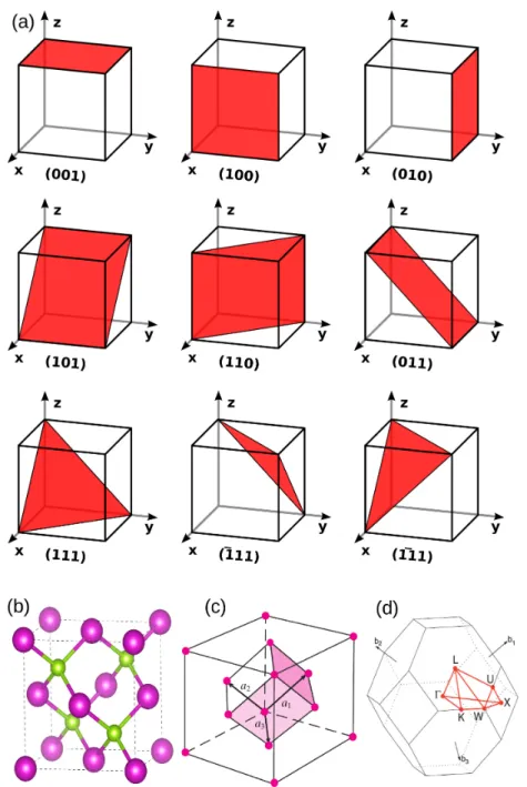
Using the first-principle calculations of density functional theory within the (FP-LAPW) method, we have investigated the structural, electronic and optical properties of Bi 2 Te 3-

The probability of attending school four our group of interest in this region increased by 6.5 percentage points after the expansion of the Bolsa Família program in 2007 and

[r]