Structural properties of nanoscopic ring systems and
their optical response
VIVALDO LOPESOLIVEIRANETO
Federal University of São Carlos Physics Department
Structural properties of nanoscopic ring systems and
their optical response
VIVALDO LOPESOLIVEIRANETO
PROF. DR. VICTORLOPEZRICHARD
Thesis presented to Physics Department of the Federal University of São Carlos - DF/UFSCar
as part of the requirements for the PhD title in Physics.
UFSCar - São Carlos/SP
Ficha catalográfica elaborada pelo DePT da Biblioteca Comunitária UFSCar Processamento Técnico
com os dados fornecidos pelo(a) autor(a)
O48s
Oliveira Neto, Vivaldo Lopes
Structural properties of nanoscopic ring systems and their optical response / Vivaldo Lopes Oliveira Neto. -- São Carlos : UFSCar, 2016.
115 p.
Tese (Doutorado) -- Universidade Federal de São Carlos, 2016.
Acknowledge
I would like to thanks:
Victor and Sergio, whereby I have great admiration, for their teachings, being patience and very friendly with me during the last years enabling the success of this project.
Nancy, Sergio, Julia and the rest of the family for receive Sarah and me wonderfully well at their house in Athens-OH, where we really felt at home, although being in another country.
All my group colleagues and professors for teachings and friendship during these years. All my work collaborators that have engaged in works resulting in some papers.
My department friends and their families: Leonilson, Nanna, Jaldair, Hugo, Raphael, Vanessa, Daniel, Maycon, Renilton, Ana Paula and Clarissa for conferences travels and friendship.
My friends out of the department (Carpas’s Club): Rafinha, Ivan, Carol, Tuti, Marcão, Zelda, Willian, Vinicius, Titi, Dinamerico, Joelma, PH, Ana, Rafael (Moh), Lu, Juninho, Pri,
Du and Fran for our meetings and celebrations together. CAPES for the financial support and sandwich stage.
There is no shortcut to success
" The separation of talent and skill is one of the
greatest misunderstood concepts for people who
are trying to excel, who have dreams, who want
to do things. Talent you have naturally. Skill in
only developed by hours and hours and hours of
beating on your craft."
Abstract
In this thesis, the electronic and structural properties of nanostructured systems were stud-ied aiming to get a realistic model for quantum rings, potentially adaptable for quantum dots.
To attain these goals, several studies supported by experimental results were carried out that allowed the introduction to the building blocks for the theoretical models such as: the envelope
function approach within the k.p approximation in quantum wells, and quantum ring/dot with perpendicular magnetic field and without spin-orbit interaction. In these models, the effects
of size, strain and localization were subsequently introduced to understand the ring formation process and their effects in the photoluminescence and magneto-photoluminescence. The
ex-perimental results of atomic force microscopy indicated the importance of structural properties and the types of asymmetries possibly found in quantum rings after the growth process. The
understanding of these effects and the evidence of the anisotropy in a preferential direction of the ring helped building more realistic models for the potential profiles. Various systems were
then studied with success. They also included a controllably magnetic field (both in magnitude and orientation), beside the geometric deformation, making the ring ellipsoidal, and taking into
account the spin-orbit interaction. The most realistic model was used to analyze the Berry phase generation and the relative weight of the contribution of each term of the Hamiltonian.
Resumo
Nesta tese de doutorado, as propriedades eletrônicas e estruturais de sistemas nano estru-turados foram estudadas visando a obtenção de um modelo realístico para anéis quânticos
po-tencialmente adaptáveis a pontos quânticos. Para alcançar este objetivo, foram feitos alguns estudos, apoiados por resultados experimentais, que permitiram a construção passo a passo do
modelo teórico, como: aproximação da função envelope na representação k.p em poços quânti-cos e anéis/pontos quântiquânti-cos com campo magnético perpendicular e sem interação spin-órbita.
Nestes modelos, os efeitos do tamanho, tensão e localização foram introduzidos subsequente-mente para entender o processo de formação do anel e os resultados apresentados na
fotolu-minescência e na magneto-lufotolu-minescência. O resultado experimental da microscopia de força atômica nos levou a analisar a importância das propriedades estruturais e os tipos possíveis de
assimetria encontrados em anéis quânticos devido ao processo de crescimento. O entendimento desses efeitos e a evidência de anisotropia em uma direção preferencial do anel ajudou na
con-strução de modelos mais realísticos para os perfis de potencial. Deste modo, vários sistemas foram estudados com sucesso. Eles também possuíam um campo magnético controlável
(am-bas, magnitude e orientação), além da deformação geométrica, que torna o anel elipsoidal, e a interação spin-órbita. O modelo mais realístico foi usado para analisar a geração da fase de
Berry e o peso da contribuição de cada termo do Hamiltoniano.
List of Figures
2.1 Scheme of a primitive cell, in blue, defined by the primitive axesv1,v2andv3. 8
2.2 Bravais lattices in three-dimensions. The vector ai and angle αi j are in: (a)
simple cubic, (b) body centered cubic and (c) faced centered cubic witha1=
a2=a3 andα12 =α23 =α31=90o; (d) simple monoclinic and (e) body
cen-tered monoclinic witha1̸=a2̸=a3,α23=α31=90oandα12̸=90o; (f) simple
orthorhombic, (g) body centered orthorhombic, (h) base centered orthorhombic
and (i) faced centered orthorhombic witha1̸=a2̸=a3andα12=α23 =α31=
90o; (j) simple tetragonal and (k) body centered tetragonal witha
1 =a2̸=a3
andα12=α23=α31=90o; (l) triclinic witha1̸=a2̸=a3andα12̸=α23̸=α31;
(m) trigonal witha1=a2=a3andα12=α23=α31<120o; and (n) hexagonal
witha1=a2̸=a3,α12 =120oandα23=α31=90o. . . 9
2.3 Scheme illustrating a unit cell containing just one atom. . . 10
2.4 Miller indices of some important planes in a cubic crystal. . . 10
2.5 Transition between valence band and conduction band. (a) Indirect transition and (b) direct transition. . . 12
2.6 The potential profile for (a) QD and (b) QR. . . 25
2.7 Scheme indicating radiusRand effective width∆(r)of the QR. . . 26
2.8 QR electronic orbitals for different values oflandn, withm=0. . . 27
2.9 Itinerary for adiabatic transport of a pendulum on the surface of the earth. . . . 29
3.1 (a) Comparison between the conduction band edges as function of strain for the profiles corresponding to the samples of InGaAs and InGaAsN quantum
well for two different sizes: 4 and 7nm. (b) Comparison between the valence subbands energies as function of strain for the profiles corresponding to the
samples of InGaAs and InGaAsN quantum well for two different sizes: 4 and 7nm. . . 37
3.2 Diagram representing the QW layer with a lateral localization core with cylin-drical symmetry. (a) Relative valence subband shift,δEhh−δElh, due to strain
effects. (b) The same shift by considering just the localization effects as a func-tion of the square aspect ratio. . . 39
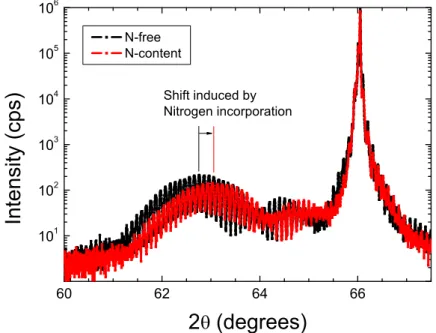
3.3 Comparison between sample N-free (black line) and N-containing QW (red line) x-ray diffraction. The shift of the red broad peak to higher angles is
in-duced by nitrogen incorporated into the two QWs [21]. . . 40 3.4 PL spectra as a function of temperature (a) InGaAs (QW) reference sample and
(b) InGaAsN (QWN) sample. [21]. . . 41 3.5 Transition energies as function of temperature. Experimental curves (dotted)
and calculated values (curves): with strain effects (solid curves) and without strain (dashed curves) [21]. . . 42
3.6 Integrated PL intensity as function of the inverse of temperature for: (a) In-GaAsN samples of 4 and 7 nm and (b) InGaAs samples of 4 and 7 nm [21]. . . 44
3.7 (a) Calculated overlap integral for a GaInAsN/GaAs QW as a function of its width, Lz. (b) Calculated overlap integral for the in-plane wavefunctions as a
function of the lateral confinement radius,R, and magnetic field [21]. . . 45
3.8 Calculated magnetic shift for: (a) the holes at the ground state of the 4 nm
InGaAs QW for various values of the in-plane strain, (b) the holes ground state in a 4 nm InGaAsN QW at a fixedε||=−1% for various values of the square
aspect ratio. (c) Calculated magnetic shift in a 4 nm InGaAsN QW for electrons, holes and electron-hh pair. The symbols represent the experimental results [21]. 46
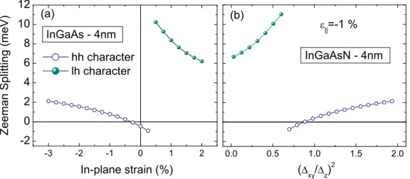
3.9 Calculated valence band ground state Zeeman splitting at 15 T for: (a)In0.36Ga0.64As
4nm as a function of the in-plane strain and (b), forIn0.36Ga0.64As0.088N0.012for
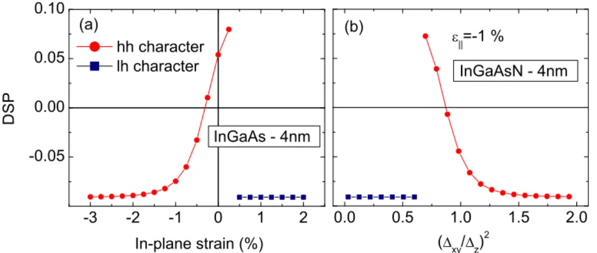
3.11 Calculated degree of spin polarization for the valence band ground state at 15 T, for: (a) the 4 nm In0.36Ga0.64As quantum well at T=2 K as a function of
the in-plane strain and (b) for the 4 nmIn0.36Ga0.64As0.088N0.012QW at a fixed
ε||=−1% as a function of the square aspect ratio [21]. . . 49
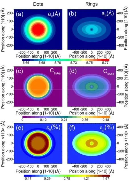
3.12 Indium and Gallium content estimations along the QR radial direction using TEM. The respective magnitudes of In and Ga were defined as relative counts:
Cont(Ga) = Count(Ga)/(count(Ga) + Count(In)) and Cont(In) = Count(In)/(count(Ga) + Count(In)) [26]. . . 50
3.13 In-plane iso-lattice parameter projections, obtained by X-ray diffraction, for QD and QR samples are shown in panels (a) and (b), respectively. Panels (c)
and (d) are representations of the In concentration for each iso-lattice parameter region from QDs and QRs. Elastic in-plane strain projections, obtained by
con-sidering the deviation from the measured lattice parameter to the relaxed alloy concentration are shown in panels (e) and (f) [26]. . . 51
3.14 Adjustment of theoretical and experimental In-content obtained. . . 52 3.15 Energy levels of hole states as a function of the effective QR radius(R) for fixed
values of the QR height (L=5 nm), QR width, ∆r=(E0
a2 )1
2
=2.29 nm, and in-plane strain value: (a)ε∥=0 and (b)ε∥=1.37%. The dominant HH or LH
characters of the energy states are indicated [26]. . . 52 3.16 Energy levels of hole states as a function of the effective QR width,∆r, for fixed
values of QR radius (R=14.75 nm), QR height (L=5 nm) and in-plane strain value: (a)ε∥=0 and (b) ε∥=1.37%. The dominant HH or LH characters of
the energy states are indicated [26]. . . 53 3.17 Main weight of expansion coefficients, Clm,n, for the valence band ground state
when expanded in the set|α,m,n,l⟩, as a function of (a) the effective QR radius
R, for fixed values of the QR width ∆r=2.29 nm and QR height L=5 nm,
and (b) the QR width ∆r for fixed values of the radiusR=14.75 nm and QR heightL=5 nm. The figures show calculations with (dashed-lines) and without
(solid-lines) strain field effects [26]. . . 54
4.1 Conduction band over magnetic field: spin up (blue lines), spin down (red lines)
4.2 First valence band levels for non hybrid circularly symmetric QR showing the main character of the ground state. . . 61
4.3 (a) Valence band electronic structure for circularly symmetric QR and its (b) ground state coefficients. . . 62
4.4 Examples of deformed QRs from images obtained experimentally by AFM [8]. 63 4.5 Potentials profiles for (a) circularly symmetric QR, and QRs deformed by
addi-tion of the terms (b)δ ρcos(ϕ), (c)δ ρ2exp[−(ϕ2η−2π)2], and (d)δ ρ2cos2(ϕ). . . 63 4.6 (upper panels) Lower conduction band states and (lower panels) its
correspond-ing ground state coefficients for QR deformed byδ ρcos(ϕ), comparingδ =0 to non vanishingδ values. The main character of the states are shown. . . 65 4.7 (a) Valence band electronic structure for a deformed QR by δ ρcos(ϕ) and its
(b) ground state coefficients. . . 65
4.8 (a) 3D wave function forδ ρcos(ϕ)case, and (b) valence band electronic orbital atB=20 T. . . 66
4.9 (a) Conduction band electronic structure modified by δ ρ2exp[−(ϕ2η−2π)2] term,
and (b) its corresponding ground state coefficients. . . 66
4.10 (a) Valence band electronic structure for a deformed QR byδ ρ2exp[−(ϕ2η−2π)2]
and its (b) ground state coefficients. . . 67
4.11 (a) 3D wave function for δ ρ2exp[−(ϕ2σ−2π)2] case, and (b) valence band
elec-tronic orbital atB=20 T. . . 67
4.12 (a) Conduction band electronic structure modified byδ ρ2cos2(ϕ)term, and (b) its corresponding ground state coefficients. . . 68
4.13 (a) Valence band electronic structure for a deformed QR byδ ρ2cos2(ϕ)and its (b) ground state coefficients. . . 68
4.15 Panel (a): AFM image of the topmost layer containing QR chains grown on an In0.4Ga0.6As/GaAs(100) vertical QD superlattice. Panel (b): Left side:
Multi-beam bright field TEM images of the hybrid multilayered sample used in this work. Right side: The FEM model of the QD/QR stack. For the out-of-plane
strain in color code shown on the right, the blue colors are related to compres-sive (negative) out-of plane strain while green/yellow/red colors denote tensile
(positive) out-of-plane strain. Panel(c): Calculated valence band deformation potential profiles for repulsive HH and attractive LH carriers in the QD region.
The position axis represented in panel (c) depicts the coordinate along the radial [xy0] direction is on the vertical distance of 0.5 nm from the islands base plane,
wherer=0 nm corresponds to the center of the QD [11]. . . 70 4.16 Different eccentricities caused byδ variation. . . 72 4.17 (a) Lateral QR profile for the two widths used in the simulations for two values
of the angle ϕ. (b) Energy levels of an eccentric QR with e=0.0234 versus
magnetic field and (c), the corresponding conduction band coefficients of the ground state. (d) Energy levels of an eccentric QR withe=0.2283 in a
mag-netic field and (e), the corresponding conduction band coefficients of the ground state. . . 73
4.18 (a) The optical transition matrix elements involving them=0 HH and LH states of a QD withR=9.48 nm and 6 nm height as a function of the magnetic field
in the parabolic band approximation. The lateral QD profiles for the HH and LH subbands with a HH in the outer rim and a LH confined inside are shown
in the inset. (b) The corresponding upper valence band and lower conduction band states (measured from above the energy gap) in a QD with HH in the outer
rim and the electrons and LH confined inside as a function of the magnetic field in the parabolic band approximation. (c) The corresponding energy levels of
a similar QD now withe=0.104 calculated within the 4×4 Luttinger model. (d) The corresponding conduction band coefficients of the ground state and the
4.19 (a) Diamagnetic shift of the exciton ground state transitions versus magnetic field. (b) Integrated PL intensities for the hybrid sample, with σ+ and σ−
polarizations measured in Faraday geometry for QDs as a function of magnetic field [11]. . . 76
5.1 Scheme of tilted magnetic field applied in a QR. . . 82
5.2 Conduction band over magnetic field: spin up (blue lines), spin down (red lines) with a tilted angle of 45◦ . . . . 84
5.3 Conduction band energy versus magnetic field orientation θ forR=17.7 nm,
L=7 nm at fixed magnetic field intensity (a)B=2.9 T, (b)B=8.8 T and (c)
B=14.7 T. Corresponding ground state expansion coefficients at (d)B=2.9 T,
(e)B=8.8 T and (f)B=14.7 T. . . 84 5.4 (a) Electronic structure and (b) ground state coefficients of a QR with
perpendic-ular magnetic field (θ =0◦) and SO coupling modulated byF =100kV/cm2.
The insets show zooms on the selected regions. . . 86
5.5 Conduction band energy versus magnetic field orientation θ forR=17.7 nm,
L=7 nm with SO coupling modulated byF =100 kV/cm2 at fixed magnetic
field intensity (a)B=14.7 T, (b)B=2.9 T. Corresponding ground state expan-sion coefficients at (c)B=14.7 T, (d)B=2.9 T. . . 87
5.6 Electronic structure for a QR in the presence of a tilted magnetic field (θ=45◦), with SO coupling and asymmetry strength modulated, respectively, byF andδ, where in (a)δ =0 andF =0, (b)δ =0 andF=100kV/cm2, (c)δ =2 meV andF =0 and (d)δ =2 meV andF=100kV/cm2. . . 88
5.7 Electronic structure for QRs in a magnetic field at fixed tilt angle,θ =60◦, and Rashba fieldF =100 kV/cm, as a function of the total magnetic field strength
for: (a) symmetric (δ =0) and (i) asymmetric (δ =2 meV) QR. The Berry phase for different levels forδ =0 is shown in panels on the left column, (b)
through (g); and for δ = 2 meV on the right column, (j) through (o). The cumulative Berry phase for different occupation numbers is shown in panel (h)
5.8 Electronic structure for QRs under fixed magnetic and Rashba fields,B=6.625 T and F = 100 kV/cm, as a function of the magnetic field tilt angle θ for: (a) symmetric (δ =0) and (i) asymmetric (δ =2 meV) QR. Berry phases for different states in both QRs are shown in the panels below. The cumulative
Berry phase for different occupations is shown in panels (h) and (p), for the symmetric and asymmetric QRs, respectively [12]. . . 90
5.9 Panels on the left column shown expansion coefficients for the four lowest states of an asymmetric QR (δ =2 meV), and fixed Rashba fieldF=100 kV/cm, and
magnetic field tilt angleθ =60◦, as function of magnetic field intensity. Level admixtures clearly evolve with sudden switches at level anticrossings. The right
column shows spin density vector maps along the QR (z-integrated) for the four
lowest states at a fieldB=2.375 T. Blue arrows have a positive projection along
z, while for red arrows the projection is negative. Notice nearly parallel vectors
in level 1 result in a null Berry phase; in contrast, canting of vectors in level 2
List of Tables
3.1 Values of Varshni’s parameters obtained by the interpolation (* α =0.4 was adjusted to the experimental curves) . . . 41
3.2 Values ofε∥used in Fig. 3.5 . . . 42 3.3 Fitted parameters obtained by Arhenius plot . . . 43
List os Abbreviations
QD Quantum Dot
QWr Quantum Wire
QR Quantum Ring
MBE Molecular Beam Epitaxy
AB Aharonov-Bohm
PL Photoluminescence
SO Spin-Orbit
QW Quantum Well
BIA Bulk Inversion Asymmetry SIA Structure Inversion Asymmetry
LH Light Hole
HH Heavy Hole
AFM Atomic Force Microscopy
HRXRD High-Resolution X-Ray Diffraction
DSP Degree of Spin Polarization TEM Transmission Electron Microscope
Contents
1 INTRODUCTION 1
2 THEORETICAL BACKGROUNDS 7
2.1 Crystal Structure and Properties . . . 7
2.2 Effective mass approach and envelope function . . . 12
2.3 K.P Method and Luttinger hamiltonian . . . 17
2.3.1 Strain Effects . . . 21
2.4 QW and QD/QR Models . . . 24
2.4.1 QW Model . . . 24
2.4.2 QD and QR model . . . 25
2.5 Geometric phase . . . 28
3 SELF-ORGANIZATION EFFECTS: Localization and Strain 34 3.1 Introduction . . . 34
3.2 Structural effects of the layers growth in the electronic structure: InGaAs and InGaAsN . . . 35
3.3 Modulation effects of strain fields on QR and QD systems . . . 49
3.4 Conclusions . . . 55
4 EXTERNAL FIELDS AND ASYMMETRY EFFECTS IN 0D STRUCTURES 59 4.1 Introduction . . . 59
4.2 Magnetic fields in confined states in 0D traps (QR) . . . 60
4.3 Asymmetry effects on conduction and valence electronic states of QRs . . . 62
4.4 Modulation effects of strain fields in elongated QD-QR stacked . . . 69
5 BERRY PHASE IN RASHBA-QR UNDER TILTED MAGNETIC FIELD 80
5.1 Introduction . . . 80
5.2 Tilted Magnetic Field in QRs . . . 82
5.3 SO Coupling . . . 84
5.4 Berry phase in asymmetric Rasha QR under tilted magnetic field . . . 87
5.5 Conclusions . . . 95
6 GENERAL CONCLUSIONS 97 A SO FIELD AND SELECTION RULES 99 A.1 SIA Hamiltonian . . . 99
A.2 Angular Momentum Selection Rules . . . 107
B TILTED MAGNETIC FIELD 108 B.1 Zeeman Splitting due to Tilted Magnetic Field . . . 109
B.2 SO Due to Tilted Magnetic Field . . . 110
C PARAMETERS OF In0.36Ga0.64As AND In0.36Ga0.64As0.088N0.012CALCULATED
BY LINEAR INTERPOLATION 112
Chapter 1
INTRODUCTION
Recent progress in nanostructure engineering has enabled foreseeing opto-electronic ap-plications of systems based on quantum dots (QDs), quantum wires (QWrs) and quantum
rings (QRs) such as low-threshold lasers [1], infrared photodetectors [2], solar cells [3], bio-sensors [4,5], spintronic gates [6], etc. In view of the wide application of QDs, QWrs, and QRs
for the creation of efficient opto-electronic devices, extensive studies have been carried out in many nanoscale structures for understanding their basic properties and the physics underneath
[7–14]. Among the possible nanostructures, the QRs present attractive features for fundamental quantum mechanics studies and applications, like terahertz detectors [15].
The nanostructures studied here were obtained by molecular beam epitaxy (MBE) [16], and in case of QRs, they are formed via the Stranski-Krastanov method [9, 10], where a very thin
cap-layer of the same material from the barrier is deposited over the QDs previously formed by MBE. After this procedure, material from the QD center is ejected and redistributed around
the QDs, creating a volcano crater-like ring nanostructure. Several studies have discussed the formation of the QRs in terms of the thermodynamic equilibrium and kinetic transition, but a
satisfactory explanation of these processes is still under scrutiny [17–22]. This unique toroidal topology displayed by the QRs has also allowed the observation of the Aharonov-Bohm (AB)
effect [23] in transport experiments [24–27].
The AB interference in type-I systems, where both electron and hole move together inside
the QR, has been found in the magneto-photoluminescence from self-assembled InGaAs/GaAs QR single layer structures [28]. It has also been shown that optical emissions from type-II
The Stranski-Krastanov growth mode has attracted both theoretical and experimental inter-est [29,30]. This method has become the main recipe for fabricating ordered arrays of QDs and
QRs. To attain self-organization of nanoscopic structures with the highest possible uniformity and geometry control, a layer-by-layer growth is indispensable. Unavoidably, a vertical stack
of nanoscopic islands is formed in this process. However, some unexpected geometric shapes could be observed in layer-by-layer growth, such as defects, making the resulting structure non
circularly symmetric. In the case of QRs, one may find elongated/elliptical structures and QRs with punctual deformations [31]. These deformations affect directly their electronic structure.
In this thesis, we aim to build a realistic and versatile model to characterize QRs and QDs systems that allows analyzing several effects, such as those produced by strain, localization,
asymmetry, spin orbit coupling, and controllable external magnetic fields. The existing mod-els [32–37] are not able to analyze such a spectrum of effects within a single framework, which
limits the study of dimensionality, for example, while our model allows verifying the combina-tion of these effects simultaneously.
We have firstly introduced the fundamental concepts within chapter 2 and then described basic effects of the growth process in semiconductor nanostructures, in chapter 3. Here, the
fundamental effects of composition, confinement, strain and localization are discussed in or-der to unor-derstand the complex nanostructure systems introduced later. To reach this goal we
have discussed optical and magneto-optical results based on our electronic structure calculation, where the relative effects of modulation are associated to structural parameters analyzed by
us-ing multiband calculations. After that, in chapter 4, we have investigated the effects of external fields and asymmetries in QRs and QD-QR stacked structures, where one InGaAs/GaAs QR
layer is grown on a vertical superlattice of InGaAs/GaAs QDs aligned laterally. This hybrid en-semble of nanostructures reveals strong optical anisotropy in the polarized photoluminescence
(PL) spectrum and unusually strong oscillations of PL intensities as a function of magnetic field in both QDs and QRs spectral emission ranges. These oscillations are observed simultaneously
and related to the Aharanov-Bohm interference patterns. Such a behavior of the magneto-PL can be understood in terms of joint effects associated to strain, spatial and magnetic
confine-ments affecting the valence band states forming the magneto-exciton ground state of the hybrid structure. And finally, in chapter 5, we have studied another QR system, where an external
In order to attain our goals, a combination of experimental results, provided by collabora-tors, and our theoretical procedures has been gathered to build an accurate framework for the
analysis.
Till now, these efforts resulted in the following published papers:
1. Berry phase and Rashba fields in quantum rings in tilted magnetic field. Physical Review B 92, 035441 (2015).
2. Carrier transfer in vertically stacked quantum ring-quantum dot chains. Journal of Ap-plied Physics 117, 154307 (2015).
3. Structural and magnetic confinement of holes in the spin-polarized emission of coupled quantum ring-quantum dot chains. Physical Review B 90, 125315 (2014).
4. Strain and localization effects in InGaAs(N) quantum wells: Tuning the magnetic re-sponse. Journal of Applied Physics 116, 233703 (2014).
Bibliography
[1] Z. I. Alferov, Rev. Mod. Phys.73, 767 (2001).
[2] H. Pettersson, J. Tragardh, A. I. Persson, L. Landin, D. Hessman, and L. Samuelson, Nano
Letters6, 229 (2006).
[3] M. Law, L. E. Greene, J. C. Johnson, R. Saykally, and P. Yang, Nature Materials4, 455
(2005).
[4] Y. Huang, X. Dong, Y. Shi, C. M. Li, L. J. Li, and P. Chen P, Nanoscale2, 1485 (2010).
[5] S. Su, Y. He, S. Song, D. Li, L. Wang, C. Fan, and S. T. Lee , Nanoscale2, 1704 (2010).
[6] P. Foldi, B. Molnar, M. G. Benedict, and F. M. Peeters, Phys. Rev. B71, 033309 (2005).
[7] Vas. P. Kunets, C. S. Furrow, T. Al. Morgan, Y. Hirono, M. E. Ware, V. G. Dorogan, Yu. I
Mazur, V. P. Kunets, and G. J. Salamo, Appl. Phys. Lett.101, 041106 (2012).
[8] Vas. P. Kunets, C. S. Furrow, M. E. Ware, L. D. de Souza, M. Benamara, M. Mortazavi,
and G. J. Salamo, J. Appl. Phys.116, 083102 (2014).
[9] J. Wu, Z. M. Wang, K. Holmes, E. Marega, Jr., Z. Zhou, H. Li, Yu. I. Mazur, and G. J.
Salamo, Appl. Phys. Lett.100, 203117 (2012).
[10] J. Wu, Z. M. Wang, K. Holmes, E. Marega, Jr., Yu I. Mazur, and G. J. Salamo, J. Nanopart.
Res.14, 919 (2012).
[11] M. D. Teodoro, V. L. Campo, Jr., V. Lopez-Richard, E. Marega, Jr., G. E. Marques, Y.
[12] V. Lopes-Oliveira, Y. I. Mazur, L. D. Souza, L. A. B. Marçal, J. Wu, M. D. Teodoro, A. Malachias, V. G. Dorogan, M. Benamara, G. G. Tarasov, E. Marega Jr., G. E. Marques,
Z. M. Wang, M. Orlita, G. J. Salamo, and V. Lopez-Richard, Phys. Rev. B 90, 125315
(2014).
[13] Y. I. Mazur, V. G. Dorogan, M. E. Ware, E. Marega Jr., P. M. Lytvyn, Z. Ya. Zhuchenko, G. G. Tarasov, and G. J. Salamo, J. Appl. Phys.112, 084314 (2012).
[14] Y. I. Mazur, V. G. Dorogan, E. Marega Jr., P. M. Lytvyn, Z. Ya. Zhuchenko, G. G. Tarasov,
and G. J. Salamo, New J. Physics11, 043022 (2009).
[15] E. Rasanen, A. Castro, J. Werschnik, A. Rubio, and E. K. U. Gross, Phys. Rev. Lett.98,
157404 (2007).
[16] L. L. Chang and K. Ploog, Molecular Beam Epitaxy and Heterostructures. Erice: Martinus
Nijhoff Publishers, 1983.
[17] V. Baranwal, G. Biassol, S. Heun, A. Locatelli, T. O. Mentes, M. N. Orti, and L. Sorba,
Phys. Rev. B80, 155328 (2009).
[18] G. Biasiol, R. Magri, S. Heun, A. Locatelli, T. O. Mentes, and L. Sorba, J. Cryst. Growth
311, 1764 (2009).
[19] G. Biasiol and S. Heun, Phys. Reports500, 117 (2011).
[20] H-S. Ling and C-P. Lee, J. Appl. Phys.102, 024314 (2007).
[21] R. Blossey and A. Lorke, Phys. Rev. E65, 021603 (2002).
[22] A. Lorke, R. J. Luyken, J. M. García, and P. M. Petroff, Jpn. J. Appl. Phys. 40, 1857
(2001).
[23] Y. Aharonov and D. Bohm, The Phys. Rev.115, 485 (1959).
[24] S. S. Buchholz, S. F. Fischer, U. Kunze, D. Reuter, and A. D. Wieck, Appl. Phys. Lett.94,
022107 (2009).
[25] D. Stepanenko, M. Lee, G. Burkard, and D. Loss, Phys. Rev. B79, 235301 (2009).
[26] T. C. G. Reusch, A. Fuhrer, M. Füchsle, B. Weber, and M. Y. Simmons, Appl. Phys. Lett.
[27] E. Ribeiro, A. O. Govorov, W. Carvalho Jr, and G. Medeiros-Ribeiro, Phys. Rev. Lett.92,
126402 (2004).
[28] M. D. Teodoro, V. L. Campo, Jr., V. Lopez-Richard, E. Marega, Jr., G. E. Marques, Y.
Galvão Gobato, F. Iikawa, M. J. S. P. Brasil, Z.Y. AbuWaar, V. G. Dorogan, Yu. I. Mazur, M. Benamara, and G. J. Salamo, Phys. Rev. Lett.104, 086401 (2010).
[29] A. O. Govorov, S. E. Ulloa, K. Karrai, and R. J. Warburton, Phys. Rev. B 66, 081309
(2002).
[30] N. A. J. M. Kleemans, I. Bominaar-Silkens, V. M. Fomin, V. N. Gladilin, D. Granados, A.G. Taboada, J. M. Garcia, P. Offermans, U. Zeitler, P.C. M. Christianen, J. C. Maan, J.
T. Devreese, and P.M. Koenraad, Phys. Rev. Lett.99, 146808 (2007).
[31] M. P. Nowak and B. Szafran, Phys. Rev. B80, 195319 (2009).
[32] W.-C. Tan and J. C. Inkson,Semicond. Sci. Technol.11, 1635-1641 (1996).
[33] S.-S. Li and J.-B. Xia, J. Appl. Phys.89, 3434 (2001).
[34] S.-S. Li and J.-B. Xia, J. Appl. Phys.91, 3227 (2002).
[35] R. Rosas, R. Riera, and J. L. Marín, J. Phys.: Condens. Matter12, 6851 (2000).
[36] N. Kim, G. Ihm, H.-S. Sim, and K. J. Chang, Phys. Rev. B60, 8767 (1999).
[37] J. M. Llorens, C. Trallero-Giner, A. García-Cristóbal, and A. Cantarero, Phys. Rev. B64,
Chapter 2
THEORETICAL BACKGROUNDS
As stated previously, this work is a theoretical study of semiconductor nanostructured sys-tems and tackles problems involving them. As they requested the interplay of various concepts
and models, this chapter is dedicated to the introduction of the general theoretical concepts used in the work. Thus, the chapter begins with a basic description of the crystal structure and
elec-tronic properties. Then, followed by the concept of effective mass and envelope function, the
k.pmethod and the Luttinger Hamiltonian are presented. They are the grounds for the
conduc-tion and valence bands simulaconduc-tions. Subsequently, the strain effects are introduced, ending with the description of the systems of interest: quantum wells (QWs), QDs, and QRs.
2.1
Crystal Structure and Properties
Crystals present special optical and electrical properties different from fluids and other
solids, which make them useful for electro-optical and electronic applications. These prop-erties, such as their band structure and conductivity, can be controlled during the crystal growth
and doping, and are widely used for manufacturing electronic devices. To describe a crystal structure, there are three important questions to answer: what kind of lattice is present? what
choice of fundamental translation vectorsv1, v2 andv3 (that define the lattice) do we wish to
make? what is the basis?
More than one lattice is always possible for a given structure, and more than one set of axes is always possible for a given lattice. The basis is identified once these choices have been
a crystal translation vector as [1]
T =u1v1+u2v2+u3v3 (2.1)
whereu1,u2andu3are arbitrary integers. A basis of atoms is attached to every lattice point, with
every basis being identical in composition, arrangement, and orientation. A crystal structure is formed by adding a basis to every lattice point.
In Fig. 2.1, one may see an example of a primitive cell (blue parallelepiped) defined by the primitive axesv1,v2,v3. A primitive cell is a type of unit cell. A cell will fill all space by the
repetition of suitable crystal translation operations. A primitive cell is a minimum-volume cell. There are many ways of choosing the primitive axes and primitive cells for a given lattice. The
number of atoms in a primitive cell or primitive basis is always the same for a given crystal structure.
Figure 2.1: Scheme of a primitive cell, in blue, defined by the primitive axesv1,v2andv3.
Bravais proved that there are only fourteen different space lattices, divided into seven crystal systems indicated in Fig. 2.2. We focus on cubic structures because that it is the symmetry of
the InAs, GaAs and their alloys, studied in this thesis.
There is always one lattice point per primitive cell. If the primitive cell is a parallelepiped
with lattice points at each of the eight corners, each lattice point is shared among eight cells, so that the total number of lattice points in the cell is one, as illustrated in Fig. 2.3, and the
volume of a parallelepiped with axesv1,v2,v3isVc=|v1·v2×v3|. The basis associated with
a primitive cell is called a primitive basis. No basis contains fewer atoms than a primitive basis
Figure 2.2: Bravais lattices in three-dimensions. The vectorai and angleαi j are in: (a) simple
cubic, (b) body centered cubic and (c) faced centered cubic witha1=a2=a3andα12=α23=
α31=90o; (d) simple monoclinic and (e) body centered monoclinic witha1̸=a2̸=a3,α23 =
α31 =90o andα12̸=90o; (f) simple orthorhombic, (g) body centered orthorhombic, (h) base
centered orthorhombic and (i) faced centered orthorhombic witha1̸=a2̸=a3andα12=α23=
α31=90o; (j) simple tetragonal and (k) body centered tetragonal witha1=a2̸=a3andα12=
α23=α31 =90o; (l) triclinic witha1̸=a2̸=a3andα12̸=α23̸=α31; (m) trigonal witha1=
a2=a3 and α12 =α23 =α31<120o; and (n) hexagonal with a1=a2̸=a3, α12=120o and
Figure 2.3: Scheme illustrating a unit cell containing just one atom.
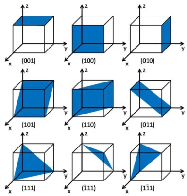
In a crystal, it is important to know its crystal planes, defined by the atoms constituting the
lattice. In semiconductor physics, knowing the crystal planes is crucial because depending on the plane the bulk substrate is cut and the samples are grown, one may obtain different properties
and results of the growth process. In Fig. 2.4, we show possible planes obtained from the bulk structure cut along different directions. The planes are usually named by the Miller indices [2]
[hkl] that indicate the direction of the normal vector to the in the basis of the corresponding reciprocal lattice.
Figure 2.4: Miller indices of some important planes in a cubic crystal.
Crystals are usually classified by their conductivity/resistivity. Thus the crystals can be
elec-trical resistivity at room temperature with values in the range of 10−2to 109ohm-cm, strongly
dependent on temperature. At absolute zero, a pure perfect crystal of most semiconductors will
be an insulator, if we arbitrarily define an insulator as having a resistivity above 1014 ohm-cm. Devices based on semiconductors include transistors, switches, diodes, photovoltaic cells,
de-tectors, and thermistors. These may be used as single circuit elements or as components of integrated circuits.
A highly purified semiconductor exhibits intrinsic conductivity, as distinguished from the impurity conductivity of less pure specimens. In the intrinsic temperature range, the electrical
properties of a semiconductor are not essentially modified by impurities in the crystal. The conduction band is void at absolute zero and is separated by an energy gapEgfrom the filled
valence band. The band gap is the energy difference between the lowest state of the conduction band and the highest state of the valence band. The lowest point in the conduction band is called
the conduction band edge and the highest point in the valence band is called the valence band edge.
As the temperature is increased, electrons are thermally excited from the valence band to the conduction band. Both the electrons in the conduction band and the vacant state or holes
left behind in the valence band contribute to the electrical conductivity [2]. The intrinsic con-ductivity and intrinsic carrier concentrations are largely controlled byEg/kBT, the ratio of the
band gap to the temperatureT, with kB being the Boltzmann constant [3]. When this ratio is
large, the concentration of intrinsic carriers will be low and also the conductivity.
The value of the band gap may be obtained from the temperature dependence of the conduc-tivity or of the carrier concentration in the intrinsic range. The carrier concentration is obtained
from measurements of the Hall voltage [4], sometimes complemented by conductivity measure-ments. Optical measurements determine whether the gap is direct or indirect. Germanium (Ge)
and silicon (Si) are examples whose the band edges are connected by indirect optical transi-tions (Fig. 2.5(a)), while in indium antimonide (InSb) and gallium arsenide (GaAs) the band
edges are connected by a direct transition (Fig. 2.5(b)). Here, we studied GaAs, indium gallium arsenide (InGaAs) and (InGaAsN) structures, all direct gap systems.
In the direct absorption process, as illustrated in Fig. 2.5(b), a photon is absorbed by with the creation of an electron in the conduction band and a hole, in the valence band. On the other
Figure 2.5: Transition between valence band and conduction band. (a) Indirect transition and (b) direct transition.
Here a direct photon transition at the energy of the minimum gap cannot satisfy the requirement
of conservation of the wavevector, because photon wavevectors are negligible at the energy range of interest.
2.2
Effective mass approach and envelope function
The approach used in this thesis to calculate the band structures is based on the idea that one electron moving in the atomic lattice, under a periodic potential, can be treated through
the effective mass concept, µ∗ [5]. This approach is described within the k.p method, based on the perturbation theory. In this method various parameters are used such as: band gap,
split-off energy, inter conduction and valence band coupling elements, etc. These parameters can be determined precisely by optical and magneto-optical experiments, or from first principle
calculations, what makes the method a versatile tool. Another advantage of the k.p method is the use of a small basis with important applications in simulations of optical, magnetic and
transport properties of semiconductors. According to the electronic states to be characterized, different approximations can be applied to this formalism. In particular, we shall use two: the
parabolic approximation for the conduction band and the Luttinger model for the valence band. Thek.p method allows the electronic structure calculation close to the Γpoint (k=0) of
into the k.p representation; (ii) reduction of the problem to an eigenvalues matrix; and (iii) introduction of approximations.
To execute these steps, we start from the Schrodinger equation
H0Ψk(r) =EkΨk(r), (2.2)
where
H0= P
2
2m0+V(r), (2.3)
P=−ih∇¯ is the linear momentum operator andm0is the mass of a free electron.
According to the Bloch theorem, the carrier movement characterization can be restricted to
the first Brillouin zone [2]. The solutions of the Schrodinger equation (2.2) for one electron in a crystal is given by "envelope function"
Ψk(r) =eik·ruk(r) (2.4)
whereuk(r)is a function with the same spatial periodicity of the crystalline lattice [6].
Writing the operatorH0in terms of the wave vectork, we have
H(k) =e−ik.rH0eik.r, (2.5)
and expanding the exponentials in Taylor series
H(k) =H0−ik.[r,Ho]−
1
2
∑
i j kikj[ri,[rj,H0]] +... (2.6) wherein the commutator[r,H0] =ih¯P/m0and[r,[r,H0]] =−h¯2δi j/m0, results inH(k) = P
2
2m0+V(r) +
¯
h2k2
2m0 +
¯
h
m0k.P. (2.7)
Applying (2.7) and (2.4) in Eq. (2.2), we get:
[
P2
2m0+V(r) +
¯
h2k2
2m0 +
¯
h m0k.P
]
unk=Enkunk, (2.8)
where k is the wave vector, the potentialV(r) is the potential in which the electron moves,
symmetry pointΓ, the terms that depend onkin Eq. (2.8) vanish. Thus, it is possible to assume
a solution for this equation ink≈0 given by
unk =
∑
m
Cmkum0. (2.9)
Inserting the solution (2.9) in Eq. (2.8), multiplying by,um0∗, and using orthogonality, we
have
∑
m
[(
En0−Enk+h¯
2k2
2m0
)
δnm+ h¯k
2m0.⟨n0|P|m0⟩
]
Cmk=0. (2.10)
The diagonalization of the Eq. (2.10) results in the dispersion relationEnk and in the expansion
coefficientsCmkfor all the values ofkand all bandsn.
Suppose that the n-th band withEn0energy is not degenerated and assume small values of
k. This allows to use the perturbation theory to get
Cn∼1; Cm=
¯
hk
2m0.
Pnm
En0−Em0, (2.11)
that, replaced in Eq. (2.10), gives a second order correction inEn0energy,
Enk=En0+h¯
2k2
2m0 +
¯
h2 m20m
∑
̸=n|Pnm.k|2
En0−Em0. (2.12)
Whenkis small, the dispersion relation of the degenerated bands is parabolic aroundΓpoint
Enk =En0+h¯
2
2
∑
i,jki 1µni j(∗)
kj, (2.13)
in which thei,jindexes refer tox,y,zandµni j(∗)to the effective mass tensor, defined as [6]
1
µni j(∗)
= 1
m0δi j+
2
m20n
∑
̸=mPnmi Pnmj
En0−Em0. (2.14)
In Eq. (2.14), the effective mass of the carrier is determined by the coupling effect with
other bands. Among remote bands, in general only one or a set of bands (degenerated) have the stronger coupling. For a semiconductor of direct gap, the valence band coupling is dominant.
If we neglect the other bands coupling, the sum in Eq. (2.12) has only one term for which the denominator is the band gap. When the gap is small, the effective mass is small too. This is the
The effective mass tensor (Eq. 2.14) takes into account only the kinetic term of the Hamil-tonian and the periodic potential of the crystalline lattice. However, if we include the SO
inter-action [7]
HSO=
¯
h
4m20c2σ·p×(∇V), (2.15)
in Eq. (2.3) the lattice periodic parts of the Bloch functions become two-component spinors
|nk⟩and the Schrodinger equation (2.8) reads
[ p2
2m0+V(r) +
¯
h2k2
2m0 +
¯
h
m0k·p+
¯
h
4m20c2(σ×∇V)·(h¯k+p) ]
|nk⟩=Enk|nk⟩, (2.16)
whereσ = (σx,σy,σz)is the vector of Pauli spin matrices andcis the speed of light.
With the notation
π=p+ h¯
4m0c2σ×∇V, (2.17)
Eq. (2.16) becomes
[
H0+HSO+
¯
h2k2
2m0 +
¯
h m0k·π
]
|nk⟩=Enk|nk⟩. (2.18)
Note that in the presence of SO interaction the spinσ is not a good quantum number. We have only a common index n for the orbital motion and the spin degree of freedom, which
classifies the bands according to the irreducible representations of the double group [6, 8]. The SO coupling has a very profound effect on the energy band structure. For example, it gives
rise to the splitting of the topmost valence band. Spin degeneracy of electron and hole states in a semiconductor is the combined effect of inversion symmetry in space and time [2]. Both
symmetry operations change the wave vectorkinto−k, but time inversion also flips the spin,
so that when we combine both we have a twofold degeneracy of the single-particle energies,
E+kandE−k. When the potential through which the carriers move is inversion-asymmetric, the
spin degeneracy is removed even in the absence of an external magnetic fieldB. We then obtain
two branches of the energy dispersion,E+k andE−k. In heterostructures, the spin splitting can
be the consequence of a bulk inversion asymmetry (BIA) of the underlying crystal, and of a
structure inversion asymmetry (SIA) of the confinement potential [9, 10]. Since the SIA term is dominant over the BIA term in confined systems as QWs, QDs, and QRs, we neglected the
The SIA spin splitting in the conduction bandΓ6is given by the Rashba term [10, 11],
HSIA=αsσ·(∇V×k), (2.19)
with a material-specific prefactorαs [12, 13], and both ∇andk polar vector as shown in
Ap-pendix A. Likewise, the vector of Pauli spin matrices is an axial vector. We see in Ref. [7] that the scalar triple product in Eq. (2.19) is the only term of first order in∇andkthat is compatible
with the symmetry of the bands.
The Rashba model (Eq. 2.19) for SIA spin splitting of electron systems is well established
in the literature. For hole systems, on the other hand, the situation is more complex because of the fourfold degeneracy of the topmost valence bandΓ8. As our objective is the analysis of
the SO effects in QR conduction band in the presence of magnetic fields, as will be discussed in chapter 5, we have neglected the SO effects in the valence band. The details about the SIA
calculations for conduction band are presented in the Appendix A. However, in the presence of a tilted magnetic field, an additional term comes out. The calculations to get the SO additional
term due to tilted magnetic field is presented in Appendix B. This configuration was used in chapter 5 for QRs systems, whose Hamiltonian is also detailed in Appendix B.
The most basic model to calculate band structure of a semiconductor is the parabolic model. In this case, we assume the effective mass tensor as isotropic rewriting the Eq. (2.13) as
Ec(k) =Eg+h¯
2k2
2µ∗
e
, (2.20)
for conduction band, and
Ev(k) =−h¯
2k2
2µ∗
h
, (2.21)
for valence band, where µe∗/h are the conduction (electron) and valence (hole) band effective masses [7].
For the conduction band, this approximation can proceed and was used for our electronic structure calculations. However, the valence band effective mass tensor in semiconductor
mate-rials has an anisotropic character and this approximation can not be adopted. For this reason, we had to use more complex approximations, considering the non parabolicity effects, anisotropy,
and coupling among light holes (LHs) and heavy holes (HHs).
As introduced previously, the electronic structure description is based on the Bloch theorem
as QWs, QWrs, QDs and QRs, where the crystalline properties still remain. In this case the envelope function approximation is used [6] and Eq. (2.10), for a potential,V(r), with smooth
variation in the crystal unit cell scale, becomes
∑
m
[(
En0−Enk+h¯
2k2
2m0 +V(r)
)
δnm+ h¯k
2m0.⟨n0|P|m0⟩
]
Cmk =0. (2.22)
Proceeding analogously as for Eqs. (2.20) and (2.21), we have
Hc=Eg+
¯
h2k2
2µ∗
e
+V(r). (2.23)
for the conduction band. Changingk (before a number), for the operator−i∇, the effective
Hamiltonian is written as
Hc=Eg−
¯
h2∇2
2µ∗
e
+V(r). (2.24)
In the presence of a magnetic field,B, the operatorPb=−ih∇¯ , should be replaced by(P+
eA/c) where e is the electron charge, and A is the vector potential, such that B =∇×A.
Besides, we should include the Zeeman contribution for the system, that results in
Hc=Eg+
1 2µ∗
e
(
P+e
cA )2
+V(r) +1
2gµB⃗B·⃗σ, (2.25)
wheregis Lande g-factor andµB the Bohr magneton.
The symmetry of a given problem defines the best way to write the operatorP. In case of
cylindrical systems, such as QDs and QRs, the problem is easily solved in cylindrical coordi-nates, soP=Prϕ+Pz, where
Prϕ =−ih¯
[ br ∂
∂r+ϕb
1
r
∂ ∂ ϕ
]
(2.26)
and
Pz=−ih¯∂/∂z. (2.27)
2.3
K.P Method and Luttinger hamiltonian
For direct gap semiconductors, the carriers (electrons and holes) occupying states close to
we take into account the interaction among bands, non parabolicity effects and spin effects, that are essential to get the electronic properties of semiconductor nanostructures. Among the
analogue matrix methods, the simplest Kane model [14, 15] results in a 8x8 Hamiltonian, that should always be used when studying materials whose energy gap does not allow neglecting
the interaction of conduction (Γ6), valence (Γ8) and split-off (Γ7) bands. However, there are
others useful approximations when some inter band coupling can be neglected: For uncoupled
conduction and valence band, we use 6x6 Luttinger-Kohn Hamiltonian, while for separated valence band description, we use a 4x4 Luttinger Hamiltonian. This last model is used when
the energetic separation between valence band and split-off is large enough to uncouple these bands, as in InGaAs and GaAs.
In this section we introduce the Luttinger model [16], based onk.pmethod. The objective is to build a simple and efficient model to calculate the valence band of semiconductors QDs
and QRs. The solution obtained in Eq. (2.10) provides the exact energy bands calculation in any point of the Brillouin zone, however the region of interest in this work, as already stated,
is around Γ point. Using the method developed by Löwdin [17], that treats the problem via perturbation theory and exact diagonalization, Luttinger got his Hamiltonian (HL) taking into
account only symmetry aspects for valence band calculation [18].
The Luttinger Hamiltonian matrix depends on the plane direction. Here, we are interesting
on the direction [001]. This direction is the same as one our experimental collaborators grew their QWs, QDs and QRs samples. The representation of the Hamiltonian for direction [001] is
the 4x4 matrix operator
HLi j=HKi j+V(r)δi j (2.28)
whereHK is the kinetic energy of holes, given by Luttinger in axial approximation [16]. This
Hamiltonian describes the valence band dispersion Γ8 and includes an applied magnetic field inzdirection. The confinement potentialV(r)is added in the diagonal elements of the HH and
LH matrixHK.
The Hamiltonian HK can be represented in a combination of eigenstates of the angular
momentum 3/2,
3 2,
3 2
⟩
= 1
2|(X+iY)↑⟩ (2.29)
3 2,
1 2
⟩
=√i
3 2,−
1 2
⟩
=√1
6|(X−iY)↑⟩+2|Z↓⟩ (2.31)
3 2,−
3 2
⟩
= i
2|(X−iY)↓⟩ (2.32)
and is written as,
HK =
ahh+↑ b− c− 0
b+ alh−↑ 0 c−
c+ 0 d−lh↓ b−
0 c+ b+ d+hh↓
. (2.33)
In this symbology, the arrows represent the spins up (↑) and down (↓), and the matrix elements
are expressed as
a± = − h¯
2
2m0(γ1∓2γ2)k 2
z−
¯
h2
4m0(γ1±γ2)(k+k−+k−k+)
+ (2±1)
2 h¯ωe
(
κ+(5±4)
4 q
)
, (2.34)
d± =a±−(2±1)
2 h¯ωe
(
κ+(5±4)
4 q
)
, (2.35)
b∓ =h¯2 √
3
4m0γ3kzk∓, (2.36)
c∓=h¯2 √
3
4m0(γ2+γ3)k
2
∓ (2.37)
where the cyclotron frequencyωe is given byωe= meB
0 and the letters q,κ andγα (α =1,2,3)
are called Luttinger parameters, determined by first-principle calculations, that define HH and
LH effective masses in the ordinary way:
µhhz =m0/(γ1−2γ2), (2.38)
µlhz =m0/(γ1+2γ2), (2.39)
µhhxy=m0/(γ1+γ2) (2.40)
and
µlhxy=m0/(γ1−γ2). (2.41)
from (L′,M,N′), as
γ1=−2m0
3¯h2(L
′+2M)−1 (2.42)
γ2=−m0
3¯h2(L
′−M) (2.43)
γ3=−m0
3¯h2N
′ (2.44)
where
L′=F′+2G; (2.45)
M=H1+H2; (2.46)
N′=F′−G+H1−H2, (2.47)
with
G= h¯
2
2m20
∑
i j|⟨x|px|nΓ3j⟩|2
Ev−En,Γ3
; (2.48)
F′= h¯
2
m20
∑
i j|⟨x|px|nΓ1j⟩|2
Ev−En,Γ1
; (2.49)
H1= h¯ 2
2m20
∑
i j|⟨x|px|nΓ5j⟩|2
Ev−En,Γ5
; (2.50)
H2= h¯
2
2m20
∑
i j|⟨x|px|nΓ4j⟩|2
Ev−En,Γ4
. (2.51)
These terms can be calculated from first principles or the parameters can also be extracted experimentally through effective mass analysis.
The operatorskmay be written in polar coordinates from Eqs. (2.26) and (2.27),
k∓=−ie∓iϕ
( ∂
∂r∓ i r
∂ ∂ ϕ ±
m0ωe
2¯h r )
, (2.52)
and
kz=−i ∂
∂z. (2.53)
HL of Eq. (2.28),
HL=
ahh+↑+V(r) b− c− 0
b+ alh−↑+V(r) 0 c−
c+ 0 d−lh↓+V(r) b−
0 c+ b+ d+hh↓+V(r)
. (2.54)
This Hamiltonian is used for valence band calculations with unstrained structures. For strained
ones we need to modify the HamiltonianHL as shown below.
2.3.1
Strain Effects
It is already known that the strain is the main factor that controls both QD and QR growth.
This strain is produced by the mismatch between lattice parameters of the surfaces. Besides, the presence of strain affects the electronic properties resulting in energy bands changes. Therefore
we must consider its effects in our calculations.
When stress is applied in a semiconductor, the crystal deformation results in energy shifts [21–
23]. Application of stress in a crystal decreases the crystalline potential symmetry,V(r), mak-ing impossible the expansion of perturbed system [23] in the old representation. However, we
can introduce a deformed coordinates system,
r′i=
∑
j
(δi j−εi j)rj, (2.55)
implying
p′i=
∑
j
(δi j+εi j)pj, (2.56)
k′i=
∑
j
(δi j+εi j)kj. (2.57)
Hereε denotes the strain tensor. The Bravais lattice of a crystal under strain in the new coordi-nates system matches to a crystal without strain in the old coordicoordi-nates system.
Going back to the old notation and doing the modification r′ → r, the deformed crystal
we can expandVε(r)in series ofε,
Vε[(1+ε)r] =V(r) +
∑
i j
Vi j(r)εi j+..., (2.58)
where
Vi j =
1 2−δi j
lim
ε→0
Vε[(1+ε)r]−V(r)
εi j
. (2.59)
Restricting ourselves to linear terms of strain, we get, instead Eq. (2.8), an expression given by
[
P2
2m0+V(r) +
¯
h2k2
2m0 +
¯
h
m0k.P+
∑
i j(
−PiPj
m0 +Vi j
)
εi j
−h¯
2
m0kεk−
2¯h m0kεP
]
unk =Enkunk. (2.60)
Solving Eq. (2.60) analogously to Eq. (2.8), we have a similar expression to Eqs. (2.20) and
(2.21), yet including the term responsible to the strain shift. The important matrix elements, proportional toε are
νi jνν′ σ σ′
=
⟨
νσ
−
PiPj
m0 +Vi j
ν′σ′
⟩
, (2.61)
called deformation potentials [7].
The connection between stress and strain was identified by Robert Hooke [24] and can be
given by the linear relation,
τi j=ci jklεi j (2.62)
where ci jkl is the fourth order elastic stiffness tensor with 81 coefficients, but depending on
the crystal symmetry, the number of coefficients can be reduced. For instance, for crystals with cubic symmetry, like zinc blende, such as InAs and GaAs, the non vanishing coefficients
are only three: c11, c12 and c44. These coefficients are known as elastic stiffness constants.
written as [25] τ11 τ22 τ33 τ23 τ31 τ12 =
c11 c12 c12 0 0 0
c12 c11 c12 0 0 0
c12 c12 c11 0 0 0
0 0 0 c44 0 0
0 0 0 0 c44 0
0 0 0 0 0 c44
× ε11 ε22 ε33
2ε23
2ε31
2ε12
. (2.63)
For a system with axial symmetry where the symmetry axis is along z (3 in the previous
notation) direction (along crystallographic direction [001] in our case), the strain components are given by,
ε11 =ε22 =ε∥, ε⊥=ε33. (2.64)
In the absence of external uniaxial stress (alongz), whereτ33=0, and according to Eq. (2.63),
we can get the relation between different components,
ε⊥=−2c12
c11 ε∥. (2.65)
The variation of parallel ε∥ and perpendicular ε⊥ strain components are responsible for the
deformation in-plane and alongz axis, respectively. Thus, when the componentε∥is positive,
ε⊥is negative; so compressing one direction expands the other. The Bir-Pikus Hamiltonian [23]
is
HLD=
ahh+↑+∆Ehh b− c− 0
b+ alh−↑+∆Elh 0 c−
c+ 0 d−lh↓+∆Elh b−
0 c+ b+ d+hh↓+∆Ehh
+V(r)δi j, (2.66)
with
∆Ehh=−(P+Q) =−
1 2
[
β1(2ε∥+ε⊥)]−β2ε∥⊥ (2.67)
for HH subband, and
∆Elh=−(P−Q) =−1
2
[
for LH subband. Besides β1 =−2av and β2=b, where av andb are defined by the material
compositions.
2.4
QW and QD/QR Models
Another important factor relative to the subbands position is the anisotropic confinement. For electronic structure description it is important to know the details about the morphology
of the system. These details are given experimentally through structural characterization tech-niques such as atomic force microscopy (AFM). The theoretical models used here are based in
structural data obtained by our experimental collaborators that characterized the systems. The 3D structures studied in this thesis allow the separation of their confinement in a
ra-dial (xy) confinement and a (z) confinement. Thus. in this section, we present the systems, the models to emulate the potential confinements, and some important properties that depend
on confinement shape and composition. We know that the composition changes the energy gap, shifting the levels [26, 27], while the confinement modifies completely the energy
behav-ior [28]. The models used in this thesis can be basically applied to QWs, QDs, QRs systems and combinations of them.
2.4.1
QW Model
The confinement in z direction, used to simulate a QW and z confinement in QD and QR, is
given by a rigid wall, with a potential profile given by
V(z) =
eFz, 0<z≤L
∞, otherwise.
(2.69)
ForF=0, the wave function for a rigid wall is given by
χl(e/h)(z) =
√
2
Lsin (
lπz
L +
lπ
2
)
, (2.70)
withl=1,2, ...andFan external electric field applied along the growth axis. The corresponding
eigenenergies are
El(e/h)=
(
l2π2h¯2 2µ(∗e/h)L2
)
whereLis the height/thickness of the QW.
2.4.2
QD and QR model
The calculation of the spectrum in the QD and QR utilizes the full diagonalization of the Hamiltonian written in the basis that considers a sufficiently large Hilbert space, truncated to
the desired accuracy. We typically consider 11 eigenstates, with angular momentum |m|<5 for each spin orientation. These are found sufficient for convergence in the entire field and
parameter range considered in this work [29].
The choice of the model used to emulate the in-plane confinement for a 0D structure was of
great importance, since we want an expression as simple as possible to be adaptable for QDs and QRs. The in-plane confinement potential chosen,V(ρ,ϕ), is characterized by [29, 30]
V(ρ,ϕ) = a1
ρ2+a2ρ
2
−2√a1a2 (2.72)
in cylindrical coordinates, while the vertical confinement is modeled by a rigid wall model as described in Eq. (2.69). The parametersa1anda2are used to define the effective confinement
and structure shape. Eq. (2.72) is used to simulate a QR on the present form while for a QD we seta1=0. Figs. 2.6(a) and 2.6(b) represent QD and QR potential profile, respectively, obtained
by Eq. (2.72).
Figure 2.6: The potential profile for (a) QD and (b) QR.
The QR radius can be calculated asRQR= (a1/a2)1/4and, once the ground state energy,E0,
is calculated, the effective width of the QR can be estimated as∆r=(E0
a2 )1
2
. Fig. 2.7 shows a scheme indicating the radius and effective width of the QR. As we can see,Rdepends ona1
RQRremains unchanged while∆rbecomes adjustable and vice-versa. For the estimation of∆r,
E0is calculated forB=0T, while the QD radius is estimate byRQD =h/(2π√2a2µ∗).
Figure 2.7: Scheme indicating radiusRand effective width∆(r)of the QR.
The solution for the 3D Schrödinger equation, Φ(ρ,θ,z), corresponding to the potential
profile in Eq. (2.72) can be found in Ref. [31] and has been used in Ref. [30] to describe the conduction band electronic structure of QRs under applied magnetic fields. The corresponding
wavefunction,ψn(e,m/h,l)(ρ,ϕ,z), is given by
ψn(e,m/h,l)(ρ,ϕ,z) =φn(,em/h)(ρ,ϕ)χl(e/h)(z)ue/h, (2.73)
whereχl(e/h)(z)is the wave function for a rigid wall of the Eq. (2.70) andue/h=|j,mj⟩are the
basis functions at the zone center in the Kane model:|1/2,±1/2⟩,|3/2,±3/2⟩and|3/2,±1/2⟩,
for electron, HH and LH states, respectively. The planar wave function has the form
φn(e,m/h)(ρ,ϕ) =
1
λ(e/h)
(
Γ[n+M(e/h)+1]
2M(e/h)n!(Γ[M
(e/h)+1])2
)1/2
×
(
ρ λ(e/h)
)M(e/h)
e−imϕ
√ 2π e
−14
(
ρ λ(e/h)
)2
×1F1
(
−n,M(e/h)+1,1
2
(
ρ/λ(e/h))2
)
, (2.74)
where 1F1 is the hypergeometric function, n =0,1,2.. is the radial quantum number, m =
are
En(e,m/h,l)=
( n+1
2+
M(e/h)
2
)
¯
hω(e/h)−m
2h¯ωc∗(e/h)
−µ
∗
(e/h)
4 ω0(e/h)2ρ02+
(
l2π2h¯2 2µ(∗e/h)L2
)
, (2.75)
withM(e/h)=
√
m2+2a1µ
∗
(e/h)
¯
h2 ,ω
∗
c(e/h)=eB/µ(∗e/h),ω0(e/h)=
√
8a2/µ(∗e/h),ω(e/h)=
√
ωc2(e/h)+ω02(e/h)
andλ(e/h)=√µ∗ h¯
(e/h)ω(e/h).
The iso-probability surfaces corresponding to lower values of the quantum numbersn,mand
l(quantum number of the confinement on the z direction) of the wave function are displayed in
Fig. 2.8. We shall use the function of the Eq. (2.73) as a basis set for the representation of the
k.pLuttinger Hamiltonian for the valence band states within the multiband envelope function
approximation
Φ(ρ,ϕ,z) =
∑
n,m,l
Cn,m,lψn,m,l(ρ,ϕ,z). (2.76)
Figure 2.8: QR electronic orbitals for different values oflandn, withm=0.
The matrix elements for QR Luttinger Hamiltonian as function of quantum number mare
shown in Appendix D.
The QW and QD/QR were used to study confinement, external fields and asymmetries
ef-fects. Besides, we use our more complex and complete QR shapes to analyze the potential effects on the geometric phase of the potential profile asymmetries, that are shown in the


![Figure 3.5: Transition energies as function of temperature. Experimental curves (dotted) and calculated values (curves): with strain effects (solid curves) and without strain (dashed curves) [21].](https://thumb-eu.123doks.com/thumbv2/123dok_br/15656665.621450/62.892.182.756.129.537/figure-transition-energies-function-temperature-experimental-calculated-effects.webp)
![Figure 3.6: Integrated PL intensity as function of the inverse of temperature for: (a) InGaAsN samples of 4 and 7 nm and (b) InGaAs samples of 4 and 7 nm [21].](https://thumb-eu.123doks.com/thumbv2/123dok_br/15656665.621450/64.892.221.715.122.604/figure-integrated-intensity-function-inverse-temperature-ingaasn-samples.webp)