1
Metal Oxide Nanostructures for Sensor Applications
D. Nunes*, A. Pimentel, A. Gonçalves, S. Pereira, R. Branquinho, P. Barquinha, E. Fortunato, and R. Martins*
i3N/CENIMAT, Department of Materials Science, Faculty of Sciences and Technology, Universidade NOVA de Lisboa, Campus de Caparica, 2829-516 Caparica
Abstract
Human health, environmental protection and safety are just a few examples of current humankind main concerns, that drive the scientific community to develop sensors able to precisely monitor and alert to possible harms in real time. Over the years, semiconductor metal oxide-based materials have been largely employed as sensors dedicated to several applications, being particularly interesting at the nanometer scale, since it is largely known that smaller crystallite size enhances sensor’s performance. Moreover, these materials are highly appealing as they can be produced by low-cost wet-chemical synthesis routes and are in general nontoxic, earth abundant and low-cost. This manuscript extensively reviews the recent developments of nanostructured semiconductor metal oxide sensors ranging from gas to humidity sensors, including ultraviolet (UV) sensors and biosensors. Zinc oxide (ZnO), titanium dioxide (TiO2),
tungsten trioxide (WO3), copper oxide (CuO and Cu2O), tin oxide (SnO and SnO2), and
vanadium oxide (VO2, V2O5)-based sensors either as nanoparticles or as continuous
films/layers are described. Their sensing properties are correlated to size, shape, presence of defects, doping elements, amongst other relevant parameters. Different techniques and methods of fabricating these materials are addressed. The review is concluded with novel approaches for functionalization and future perspectives for sensor developments.
Keywords: semiconductor metal oxides; low-cost materials; nanostructures; sensors;
sensing properties.
*Corresponding Authors: Rodrigo Martins and Daniela Nunes, i3N/CENIMAT,
Department of Materials Science, Faculty of Science and Technology, Universidade NOVA de Lisboa, Campus de Caparica, 2829-516 Caparica, Portugal, Tel: (+351) 212948562, Fax: (+351) 21 294 8558, e-mails: [email protected] (R. Martins); [email protected] (D. Nunes).
2 Outline
1. Introduction ... 3
1.1 Metal oxide nanomaterials ... 3
1.2 Sensors for different applications ... 6
1.3 Sensing mechanisms ... 11
2. Semiconductor metal oxide nanostructures ... 18
2.1 Zinc oxide ... 18 2.2 Titanium dioxide ... 32 2.3 Tungsten trioxide ... 41 2.4 Copper oxides ... 53 2.5 Tin oxide ... 63 2.6 Vanadium oxide ... 74
3. Overview of the metal oxide sensors performance ... 83
4. Field-effect transistor structures for sensing applications ... 92
4.1. Advantages and challenges of sensing with (oxide nanostructure) field-effect transistors ... 92
4.2. Gas sensing with oxide nanowire field-effect transistors ... 95
5. Conclusions and future perspectives ... 99
3
1. Introduction
1.1 Metal oxide nanomaterials
Nanotechnology is compromised as a group of novel technologies capable of designing, producing, characterizing and controlling structures, materials, devices and systems at the nanometer scale, i.e. less than 100 nanometres. This term is very transversal, being used across many fields, such as chemistry, medicine, biology, physics, materials science, environment, engineering, amongst others. The structures or materials at the nanometer scale can be classified as: 0D (zero dimension) if all three spatial dimensions are in the nanometric range, i.e. nanoparticles or clusters; 1D (one dimension) if two dimensions are in the nanometric range, like nanotubes, nanorods and nanowires; or 2D (two dimensions) if only one spatial dimension is nanometric, such as in thin films or nanosheets. 3D (three dimensional) materials implies that the 0D, 1D and 2D elements are in close contact forming interfaces, for example compact polycrystals with nanosized grains or 3D porous nanostructures (Figure 1) [1].
Figure 1. Scheme of the types of nanostructured materials based on their dimensions: 0D, 1D, 2D and 3D
4 Nanosized materials possess unique and enhanced chemical, physical and mechanical properties when compared to their bulk counterparts due to their high specific surface area and surface-to-volume ratio [2-4]. Generally, the high surface-to-volume ratio of nanomaterials increases as nanoparticle size decreases [5]. Moreover, the size reduction of materials gives rise to quantum confinement phenomena, which modify their intrinsic properties with respect to their corresponding bulk materials [6]. Nanomaterials can occur in several morphologies ranging from nanorods, nanowires, nanowhiskers, nanoflakes, nanocubes, nanopillars, nanospheres, and others [3, 7, 8]. Carbon-based, metal, ceramic, polymeric and metal oxide nanoparticles are well-known classes of nanoparticles [3]. The latter are largely investigated since these are earth abundant, environmentally benign, low cost and, in some cases, chemically stable with suitable electrical and optical characteristics [9-16]. Moreover, these materials display exceptional properties that include mechanical stress tolerance, high optical transparency, high carrier mobilities, wide band gap, high dielectric constant, superconductivity, amongst others [16, 17]. Metal oxides are ionic compounds composed by positive metallic and negative oxygen ions [16], and can exhibit metallic, semiconductor or insulator characteristics [18]. In metal oxides, although the s-shells of positive metallic ions are always fully filled by electrons, their d-shells may not be completely filled [19]. Semiconductor metal oxides can either be classified as n-type, in which electrons are the majority charge carriers, or
p-type, in which the majority charge carriers are holes.
Metal oxide electronic, physical and chemical properties can be engineered by modifying their size, structure, composition, stoichiometry and by doping [4, 20]. Nevertheless, the electronic structure range of these materials is extensive, being divided into two main categories, i.e. transition and non-transition metal oxides, where the latter englobes the pre- and post-transition metal oxides. Transition metal oxides are known to
5 have small energy difference between a cation dn and either a dn+1 or dn−1 configuration, which allows a fast transformation between the different forms, however with unstable structures. Metal oxides with d0 and d10 electronic configurations are characterized as
materials with stable properties. The d0 configuration is found in transition-metal oxides such as, TiO2, V2O5 and WO3, whereas d10 configuration is found in post-transition-metal
oxides, as ZnO or SnO2. Regarding the pre-transition-metal oxides, these are expected
to be inert in several applications, since these have large band gaps, electrons and holes are hardly formed [21]. In general, nanoparticles of metal oxides have high density of corner or edge surface sites [22].
Over the years, semiconductor metal oxides have been extensively studied for applications ranging from solar cells [23-26], passing through their integration in electrochromic devices [27-30], lithium-ion batteries [31-33], photocatalyst agents [9, 10, 14, 34-38] and as sensors [39-42]. The interest on the latter application with semiconductor metal oxides has been reported half a century ago and has been increasing along the years due to their practical applications in everyday life, as well as in environmental protection, bio detection, to name just a few. Nowadays, semiconductor metal oxide nanostructures are widely chosen to be integrated in sensors due to their exceptional intrinsic properties associated to their high surface-to-volume ratios, high surface reaction activity, high catalytic efficiency, strong adsorption ability, and electron and phonon confinements [43]. Gas sensors are amongst the most common sensing devices, in which semiconducting metal oxides are frequently used as gas-sensing materials [44]. Another type of sensor where metal oxides are largely present are humidity sensors, which normally determine the amount of water vapor present in a gas that can be a mixture, such as air, or a pure gas, such as nitrogen or argon [45]. UV photosensors/photodetectors are also frequently used in terms of sun/UV exposure, as
6 well in environmental safety, flame detection, among others [46]. And finally, biosensors that are designed to have a fast response, be low-cost and portable in both clinical and non-clinical applications [47].
1.2 Sensors for different applications
Detection systems for monitoring air and water quality using semiconductor metal oxides are of great interest to improve the selectivity and sensitivity of current sensing devices, and at the same time allowing simultaneous measurements of numerous parameters with real-time response [48]. In the literature, application of metal oxides in gas sensors is vast, with several studies reporting the advantages of integrating these materials in such devices, as well as their gas sensing performance in respect to the size properties [21, 44, 49-52].
The gas sensing technology is largely spread in different industrial fields, but also in domestic environments, some examples are the automotive industry, for indoor air quality control, greenhouse gas monitoring, among others [52]. The most important parameters of gas sensor devices are their sensitivity, operating temperature, selectivity, long-term stability, energy consumption, reversibility, low humidity dependence and finally production cost [44, 52]. Thus, for these devices to be commercially viable, they must be stable during operation, with a uniform and reproducible signal for a prolonged period of time, despite being able to precisely detect a specific gas even in mixtures of different gases. Moreover, the precise control of metal oxide electronic and structural properties, including grain size distribution, local doping, grain boundaries and surface states is mandatory to obtain optimized performance of such devices [53].
Liu et al. [52] has classified gas sensors based on their sensing methods in two groups: (a) methods based on variation of electrical properties and (b) methods based on variation of other properties. Semiconductor metal oxide gas sensing relies on the
7 variation of electrical properties [49]. Gas sensors based on ZnO, TiO2, SnO/SnO2, WO3,
CuO/Cu2O, and V2O5 are commonly used to detect combustible, reducing, and oxidizing
gases [41, 52, 54-59], and sensing is mainly based on the resistance change responses to the target gases [52]. SnO2 followed by WO3 (Figure 2 (a)) are the most commonly used
semiconducting metal oxides in commercial gas sensors [60]. In general, reducing gases, such as H2S, NH3, CO, H2, SO2, CH4, and HCHO cause an increase of conductivity in
n-type semiconductors and a decrease in p-n-type semiconductors, while the opposite effect is observed for oxidizing gases (NO, N2O, NO2, CO2, O3 and Cl2) [61, 62].
Humidity sensors have been receiving a lot of attention in industrial, medical and even in domestic environments for human comfort. For example, these devices are employed in microelectronic and automobile industries, but also in the pharmaceutical field, food processing, humidity control in hospitals and houses, among other applications [45]. The humidity sensor performance is directly related to the properties of the sensing material including porosity, surface area, pore size distribution and morphology [63]. In similarity to the gas sensors, these devices are expected to have constant response, high sensitivity, fast response time, negligible hysteresis, chemical and physical stability, wide operating humidity range and low cost [64].
There are several humidity evaluation terms, nevertheless the most accepted are absolute and relative humidity (RH), where the latter is normally described. Per million by weight (PPMw) or volume (PPMv) and dew/frost point (D/F PT) are subclasses of
absolute humidity [45, 65]. Generally, RH is temperature dependent, and can be described by Equation 1 [65]:
𝑅𝐻 =𝑃𝑉
𝑃𝑆x 100 (1)
where PV is the actual partial pressure of water vapor present in a gas and PS is the
8 largely commercialized and can be categorized into three classes, i.e. ceramic-based sensors, organic polymer-based sensors, and organic/inorganic hybrid sensors (polymer/ceramic). Ceramic-based sensors can be designed using either semiconducting or dielectric metal oxide materials. Moreover, these sensors are divided into two groups in accordance to their sensing mechanisms, i.e. impedance (resistive) or capacitive categories, in which the former uses the conductance, and the latter, the capacitance properties of the sensing layer. Impedance-based sensors are subdivided into ionic-conduction and electronic-ionic-conduction. The p-n heterojunction humidity sensors are also included in ceramic-based sensors [65]. Different approaches have also been suggested, in which an integrated solution having a humidity sensor chip that contains humidity sensors of capacitive type is shown on Figure 2 (b) [66].
Another kind of devices that have recently drawn growing attention are UV sensors/photodetectors, which are interesting for everyday life in terms of sun/UV irradiation exposure, but also for environmental safety, medicine, military defence, flame detection, environmental sensors, space exploration, among others [67, 68]. UV photodetectors detect light in the ultraviolet wavelength ranging from 100 nm to 400 nm.
A high-performance photodetector must have high sensitivity and spectral selectivity, as well as a fast and linear response speed, together with high light transmission and improved chemical and physical stability [69, 70]. The most important parameters of photodetectors are sensitivity, responsivity and external quantum efficiency (EQE) [69]. These parameters are normally used to categorize the UV sensor performance. UV photodetector sensitivity is given by Equation (2) [69], while the responsivity is estimated according to the Equation (3) [13, 71]. The external quantum efficiency, which is defined as the number of electrons detected per light photon, [69, 72] can be obtained by Equation (4).
9 𝑆 = 𝛥𝐼 𝐼𝑑𝑎𝑟𝑘x 100 (2) 𝑅 = 𝛥𝐼 𝑃𝑈𝑉 (3) 𝐸𝑄𝐸 =ℎ𝑐 𝑒𝜆. 𝐼𝑝ℎ−𝐼𝑑𝑎𝑟𝑘 𝑃𝑈𝑉 (4)
where ΔI is the difference between the photocurrent and the dark current, Idark is the dark
current, and PUV is the UV light power, h is Planck’s constant, c is the speed of light in
vacuum, e is the electron charge, and λ is the exciting wavelength. Several photodetectors types have been reported, including photoconductors, metal-semiconductor-metal (MSM) photodetectors, Schottky photodiodes and p-n junction photodiodes. A photoconductor is composed by a semiconductor material with two ohmic contacts, forming a radiation-sensitive resistor. MSM photodiodes are based on two back-to-back Schottky diodes and using an interdigitated electrode configuration on top of the active layer. Schottky diodes consist of a metal layer that contacts a semiconductor material, and the metal/semiconductor junctions exhibit rectifying behaviour. p-n junction photodiodes are based on a heterojunction of a p- and n- type materials, without the requirement of a reverse bias and displaying improved noise performance [73]. The p-i-n has an intrinsic layer and provides additional sensitivity and performance over that of the basic p-n junction photodiode due to the reveres bias operation. Nevertheless, innovative approaches to extract the best photodetector performance, more recently with nanostructured metal oxides, are under constant development (Figure 2 (c)).
Metal oxide nanostructures are also widely present in biosensors. A biosensor is described as a sensing device that combines a transducer for signal detection with a biologically sensitive and selective component, i.e. bioreceptor (antibody, enzyme, receptor protein, nucleic acid, whole cell or tissue section). Typically enzymes are used as bio component, and they are large protein molecules that act as a catalyst in chemical
10 reactions, remaining unchanged during the process [74]. Upon interaction of a target molecule with the bio component, a signal is generated and detected by the transducer (Figure 2 (d) [75]). It is possible to occur optical or electrical signals [76]
.
This signal is proportional to the concentration of the component. The target molecules/analytes can be proteins, DNA, glucose, cholesterol, toxins, hormones, bacteria, among others [77]. These devices are considered a powerful analytical tool in medical diagnostics with the fast and precise detection of diseases, virus , food quality and safety, fermentation industry, in metabolic engineering and other areas [47, 78]. The device is expected to be highly accurate, homogeneous and reproducible, despite having optimized response time, high stability, sensitivity, specificity, selectivity (low interference) and bioactivity [76, 79].There are many types of biosensors, in which these are mainly classified according to bioreceptors and transducers. The most common are immunosensors, calorimetric, DNA, enzyme-based, tissue-based, optical, thermal, optical, piezoelectric and electrochemical biosensors, in which the latter is subdivided in conductimetric, amperometric and potentiometric sensors [74, 78]. The most successful commercial biosensor is the amperometric glucose biosensor, with which diabetic patients are able to periodically monitor blood glucose levels [74]. Nevertheless, the full integration of metal oxides nanostructures in biosensors still raises questions regarding the maintenance of their bioactivity for extended periods of time and their toxicity.
11 Figure 2. (a) Gas sensor and its respectively gas sensing characteristics for NO2 [80], (b) integrated
humidity sensor [66], (c) photoresponse characteristics of a UV photodetector [81] and (d) biosensor
detection process [75]. Reproduced with permission of Elsevier [80], MDPI [66], Springer Nature [81],
and Intech (2018) [75].
1.3 Sensing mechanisms
The mechanisms responsible for gas, humidity and UV responses have similar concepts. Despite being a controversial topic, the mostly accepted mechanism for these sensors is resultant of a change in electrical conductivity or resistivity of the semiconductor metal oxide materials [82, 83]. In the case of gas sensors, the gas sensing is resultant of a shift on equilibrium of the surface chemisorbed oxygen reaction due to the presence of a target gas, creating extrinsic surface acceptor states that immobilize conduction band electrons from the near-surface region of an n-type semiconductor material. For p-type semiconductor materials, the chemisorption of oxygen leads to an accumulation surface layer which alters their conductance [44, 61]. Under ambient conditions, the oxygen molecules are adsorbed on surface of the n-type
12 semiconductor materials and can capture inner free electrons from of these materials. The negative charge trapped in these oxygen species causes a depletion layer near the surface, which results in the reduction of the conduction layer [O2(g) + e- → O2-(ads)] [71, 82]. When
the sensor is exposed to reducing or oxidizing gases, this will affect the density of charge carriers (n-type electrons or p-type holes) in the near-surface region of each grain. Reducing gas molecules will remove surface-bound oxygen atoms, releasing immobilised electrons, whereas oxidising gases immobilise conduction-band electrons from the near-surface region by creating additional near-surface-acceptor states.Thus, the gas molecules will result in the decrease or increase of the depletion layer thickness by changing the surface-state density, which in consequence leads to a change in the materials’ conductance [44].
In summary, upon interaction with oxidizing gases, the gas species will act as acceptors, which will lead to a resistance increase for n-type semiconductor metal oxides. When the oxidizing gases are adsorbed on n-type material surface, it will gain electrons from the adsorbed oxygen, which will increase the depletion region, and thus decrease its conductivity [39]. The opposite behaviour is observed for p-type metal oxide materials. Figure 3 (a) shows the negative surface charge causing the upward band bending of conduction (EC) and valence (Ev) bands, the electron depleted region (space-charge
layer), the average thickness, i.e. the depth of band bending region (q.Vs), and the effective surface potential barrier (eV). The depth and height (eV) of the band bending depend on the overall surface charge present (amount and type of adsorbed oxygen). In Figure 3 (b), it is represented the grain boundary structures and corresponding band models showing the electron conduction mechanism. In polycrystalline sensing materials, the electronic conductivity occurs through the percolation paths along grain-to-grain contacts depending on the value of potential barrier (eV) or Schottky barrier of the surrounding grains. Upon gas exposure, the Schottky barrier between two grains is
13 lowered facilitating the electronic conduction in sensing layers through different grains via grain to grain percolation path [84].
In fact, the gas adsorption on the surface and the change in the resistance of metal oxide semiconductors are quite complex processes. It has been accepted that the sensor resistance is a function of the gas partial pressure, following a power-law response, in which the power-law exponent is specific to the gas and temperature used [85-87]. Several studies have extensively discussed the processes, including when using metal oxide nanostructures. In the case of metal oxide nanowires, the conductivity for n- and p- type materials, Equations 6 and 7, respectively, can be described as [88, 89]:
𝐺𝑛 = 𝜎𝑑 ℓ 𝜋 ( 𝐷 2 − 𝐿𝐷𝑛) 2 = 𝑁𝑑𝑞𝜇𝑛𝜋(𝐷−2𝐿𝐷𝑛)2 4ℓ (6) 𝐺𝑝 = 𝜎𝑎 ℓ 𝜋 (( 𝐷 2) 2 − (𝐷 2− 𝐿𝐷𝑝) 2 ) = 𝑁𝑎𝑞𝜇𝑝 𝜋(𝐷𝐿𝐷𝑝−𝐿2𝐷𝑝) ℓ (7)
where σ = qμN is the conductivity of the nanowire; D is its diameter; ℓ is the length; N is the carrier concentration; μ is the carrier mobility; q is the carrier charge; and LDn and LDp are the thicknesses of the depletion and accumulation layers,
respectively.
The gas-sensing response for n-type (Equation 8, (𝑆𝑂𝑋𝑛 )) and p-type (Equation 9,
(𝑆𝑂𝑋𝑝 )) semiconducting metal oxide to an oxidizing gas can be defined as [62]: 𝑆𝑂𝑋𝑛 =
𝑅𝑜𝑔
𝑅𝑎 (8)
𝑆𝑂𝑋𝑝 = 𝑅𝑎
𝑅𝑜𝑔 (9)
where Rog and Ra are the sensor electrical resistances measured with an oxidizing gas and
pure dry air, respectively.
In the case of reducing gases, the gas species act as donors, i.e. electrons will be injected into n-type material surface, reducing the depletion region and releasing the band bending, and this will lead to a resistance decrease in the case of n-type materials and
14 increase for p-type materials [39, 61]. The gas-sensing response for n-type (Equation 10, (𝑆𝑟𝑑𝑛 )) and p-type (Equation 11, (𝑆𝑟𝑑
𝑝
)) semiconducting metal oxide to a reducing gas is normally represented as [62]:
𝑆𝑟𝑑𝑛 = 𝑅𝑎
𝑅𝑟𝑔 (10)
𝑆𝑟𝑑𝑝 = 𝑅𝑟𝑔
𝑅𝑎 (11)
where Rrg and Ra are the sensor electrical resistances measured with an reducing gas and
pure dry air, respectively.
Mechanisms of water vapor adsorption on metal oxide surfaces have been well studied [45, 90, 91], and it is known that most metal oxides have adsorbed hydroxyl groups on their surface which influences the surface phenomena, including the response of a sensor to the detected gas [92]. In general, water molecules can be adsorbed by an acid-base type dissociative chemisorption followed by hydrogen bonded physisorption, however some oxides can also chemisorb water vapor through redox reactions involving electron transfer to the metal oxide [63, 92]. Moreover, water molecules have been reported to increase the conductivity of n-type semiconductor metal oxides and to decrease the conductivity of p-type semiconductor metal oxides, in which this effect was related to the donation of electrons from the chemically adsorbed water molecules to the oxide surface [67, 91].
The mechanism of all the ceramic humidity sensors, of ionic and electronic conduction (resistive) types and capacitive, depends on the superficial water vapour adsorption, which is based on chemical and physical adsorptions and capillary condensation processes. Resistivity-type humidity sensors measure the electrical resistance in response to humidity. Most of the available humidity sensors utilize the ionic type humidity-sensing mechanism. In ionic sensing devices, when the ceramic surfaces adsorb water, their electrical properties change, and by increasing the humidity, the
15 conductivity increases and thus the dielectric constant increases [65, 93]. On the other hand, capacitive-type humidity sensor mechanism relies on electrical permittivity that is sensitive to humidity variation, and the electrical response is linked to water adsorption-desorption processes on the exposed surface of the sensing material [94].
The UV sensing process occurs when the semiconductor metal oxide with oxygen molecules adsorbed on its surface and without any UV irradiation, can capture free electrons present in the n-type semiconductor and form a low conductivity depletion layer in the near-surface region. When exposed to UV irradiation at a photon energy above the materials’ band gap, electron-hole pairs are photogenerated [hν → e− + h+], and the holes migrate to the surface along the potential slope. This potential slope is produced by band bending and discharge of negatively charged adsorbed oxygen ions through surface electron-hole recombination, leading to oxygen photo desorption [95] [h+ + O2-(ads) → O2(g)] (Figures 3 (c) and (d)). This hole-trapping mechanism through oxygen adsorption
and desorption enhances the high density of trap states due to the dangling bonds at the surface and thus enhances the photoresponse [96]. The stability and performance of UV sensors are highly influenced by the surrounding environment. Several studies reported that the photodetection of metal oxide nanostructured sensors is strongly dependent on the ambient gas conditions, with significant differences regarding measurements in air, vacuum or inert gases [97-99].
16 Figure 3. (a) Scheme of the band bending in a wide band gap semiconductor after chemisorption of
charged species on surface sites (EC and EV are the conduction and valence band energies in the grain
bulk, respectively, EF is the Fermi level, e– is the conducting electrons and + the donor positions [49,
85]. (b) Schemes of the structural and band models of a n-type semiconductor, and (c) and (b) dark and
UV irradiation processes [71, 88]. Reproduced with permission MDPI [71], and Elsevier [49], [85] and
[88] (2018).
Regarding biosensors, as previously described, the devices combine a biological element with a transducer to detect specific target analytes and thus produce quantifiable and processable signals [47, 77, 100]. Generally, the measurement of electrical properties in biological systems is from electrochemical nature, in which the bioelectrochemical element will act as the main transduction element. Moreover, for electrochemical detection, enzymes are mostly used, due to their specific binding capabilities and biocatalytic activity. Antibodies, antibody fragments or antigens are usually used in immunosensor to monitor binding events in bioelectrochemical reactions [100]. These electrochemical detection techniques can generate a measurable current (amperometric),
17 a measurable potential or charge accumulation (potentiometric), or change in the medium conductive properties between electrodes (conductometric), but also measurements as function of impedance, both resistance and reactance (impedimetric), and using transistor technology (field-effect) to measure current as a result of a potentiometric effect at a gate electrode [100].
Recently, metal oxide materials have been integrated in novel biosensing devices, since they exhibit enhanced electron-transfer kinetics and strong adsorption capability. These properties guarantee appropriate microenvironments for the immobilization of bio molecules and result in enhanced electron transfer and improved biosensing characteristics. The biosensing process involving metal oxide materials relies on the biomolecules binding to these materials via physical adsorption or chemical binding. Physical adsorption of a biomolecule depends on several parameters such as surface morphology, reaction medium and net surface charge, especially when it arises due to weak interactions, such as van der Waals, electrostatic and physisorption. Nevertheless, short-range forces including charge, steric, depletion and solvent interactions can also affect the biointerface. An effective biointerface with metal oxide materials guarantees an enhanced electron transfer rate and assists the biomolecule to maintain a stable biological activity [47]. It has also been reported that adding metal oxides to unlike surfaces can increase the adhesion of negatively-charged bacteria due to their positive charge and hydrophobicity, this is of particular importance for producing high performance biosensing devices [101].
This review will address the two main types of nanostructured semiconducting metal oxide sensors including n-type, i.e. zinc oxide, titanium dioxide, tungsten oxide, tin dioxide, and vanadium oxides, but also materials displaying p-type characteristics, i.e. copper oxides and tin monoxide. Their sensing properties, production techniques and
18 methods will be discussed from an application-oriented perspective. An overview on different sensors such as gas, humidity, UV and biosensors having these nanomaterials integrated will also be presented.
2. Semiconductor metal oxide nanostructures
Semiconductor metal oxides have been largely employed in electronics and opto-electronics with their incorporation on transistors, circuits, or panel displays, and more recently on printed and paper electronics [102-104]. Nevertheless, the sensing technology has evolved over the last years and continues to grow to guarantee human well-being, quality and safety from food to air, but also for environmental protection. ZnO, TiO2,
WO3, CuO/Cu2O, SnO/SnO2 and VO2/V2O5 are examples of such materials and have
been integrated in several kinds of sensors, e.g. gas, humidity, UV and biological sensors. These materials can adopt the most distinct structures at the nanoscale, ranging from nanowires to nanospheres or nanosheets, which will directly influence their performance in the final sensing applications.
2.1 Zinc oxide
Zinc oxide has been extensively studied since 1935 due to its integration in several applications with special interest in ZnO-based electronic and optoelectronic devices. ZnO is an n-type semiconductor with a wide band gap of 3.2-3.4 eV and a large exciton binding energy of 60 meV at room temperature [105]. At room temperature and pressure, ZnO crystallizes in the hexagonal wurtzite structure in which each anion is surrounded by four cations at the corner of a tetrahedron [105]. Other structures may appear like “zinc
blend” (the term is originated from compounds like ZnS that can present cubic or
hexagonal phases) and “rocksalt” (with a cubic phase) but, under ambient conditions they are not thermodynamically stable phases. Hexagonal ZnO wurtzite structure has a unit cell with lattice constants a= 0.3296 nm and c= 0.52065 nm [106] and ratio c/a = 1.602,
19 corresponding to P63mc space group [105, 107]. This ZnO space group is characterized
by presenting two interconnecting sublattices of Zn2+ and O2- ions in which each zinc ion is surrounded by a tetrahedral of four oxygen ions [105]. The zinc and oxygen ions are arranged alternatively along the c-axis and exhibit positive and negative polar plane rich in Zn2+ and O2-, respectively. This Zn2+ and O2- tetrahedral coordination is the origin of a polar symmetry along the hexagonal axis [105, 108]. This asymmetry along the c-axis is responsible by an anisotropic growth of 1D ZnO crystallites. The most common and stable ZnO crystal exhibit a wurtzite structure with four face terminations – the polar Zn terminated (0001) and O terminated (0001̅) facets, and the non-polar (101̅0) facets, containing equal number of Zn and O atoms [14, 105, 108-110]. Figure 4, shows a schematic representation of the ZnO hexagonal wurtzite structure facets and an atomic model of the polar and non-polar facets.
Figure 4. (a) Schematic of the unit cell of the ZnO hexagonal wurtzite structure and the correspondent ionic
position of Zn2+ and O2- [107]; (b) and (c) Side view of ZnO wurtzite facets with (0001) Zn and (0001̅) O
termination, respectively [111]. Reproduced with permission of Springer Nature [107] and the Royal
20 It is well known that polar facets possess different chemical and physical properties from non-polar facets, and that O terminated polar facets also present a slightly different electronic structure [105]. These characteristics are responsible for the vast properties presented by ZnO such as piezoelectricity and spontaneous polarization, being a key factor in crystal growth and in defect generation [105].
When used in gas sensing or in other applications, it has been found that the polar Zn terminated (0001) facets are more active than polar O terminated (0001̅) and the non-polar (101̅0) facets due to the abundance of OH- that adheres to low-coordinated Zn sites,
forming highly active OH radicals [111, 112].
The growth of different ZnO nanostructures has been reported by several authors in the past few years. Different synthesis methods can be employed to produce ZnO nanostructures, such as chemical bath deposition, electrospinning, electrodeposition, laser assisted flow deposition (LAFD) and also hydrothermal/solvothermal synthesis, either by conventional or by microwave assisted heating [13, 14, 113-123]. Depending on the synthesis method, precursors used and their concentration, solution pH or even the solvents selected, zinc oxide may present different nanostructures ranging from nanorods, nanofibers, nanoneedles, nanowires, nanoplates, nanostars, tetrapods to nanoflowers [14, 108, 113, 124-127], as shown in Figure 5.
21 Figure 5. Different ZnO morphologies produced by different synthesis techniques: (a), (b) and (c) chemical
bath deposition [113]; (d), (e) and (f) electrodeposition [123, 128, 129]; (g), (h) and (i)
hydrothermal/solvothermal synthesis [112, 130]; (j) and (k) electrospinning [116, 117] and (l) laser assisted
flow deposition [121]. Reproduced with permission of Elsevier [112, 113, 116-118, 121, 123, 128, 129]
and Royal Society of Chemistry (2018) [130].
Zinc oxide is an inexpensive and earth abundant material, nontoxic and chemically stable, which makes it suitable to be used in several applications, such as field effect transistors [131-134], solar cells [121, 135-137], piezoelectric generators [138-140], photocatalysis [14, 141, 142], as a platform for SERS applications [143, 144] and in sensors [13, 71, 122, 145].
Metal oxides semiconductors are commonly used as gas sensors in environmental monitoring and in industrial applications allowing the production of low cost and small devices [146]. ZnO is capable to detect a great variety of different gases, such as CO2,
22 importance for human life. The use of inexpensive and highly sensitive miniaturized sensors are of great interest for environmental control of indoor air quality and pollution (considering the impact of CO2 emissions on the global warming) [147].
The most recent studies are focused on devices miniaturization allied to increased sensitivity. So, many authors are studying the influence of ZnO morphology on gas detection since just by changing its shape it is possible to enhance sensor performance, opening new ways to produce more selective gas sensors [150]. Gupta et al. [146] studied the sensitivity of different ZnO nanostructures, nanowires, nanobelts and tetrapods in the detection of H2S and NO. Gupta found that sensors based on ZnO nanobelts were more
sensitive to NO gas, and that ZnO tetrapods were more sensitive in detecting H2S gas
while ZnO nanowires had no response in detecting NO, H2S, NH3, CO and CH4. The high
sensitivity of nanobelts to these gases may be due to their low thickness (< 20 nm) when compared to the nanowire’s diameter ( 100 nm), thus presenting a larger surface to volume ratio. It was found that the response mechanism to detect H2S arises from changes
in the grain boundary resistance, while for the detection of NO it arises from changes in the grain boundary and intragrain resistances [146].
Jonca et al. [150] studied the use of cloudy-like, isotropic and nanorods ZnO nanostructures for detection of CO, NH3 and C3H8 gases. The ZnO nanorods
nanostructures presented higher sensitivity to the detection of this type of gases.
Nitrogen oxide gases like NO and NO2 are environmentally harmful gases formed
during the combustion in automotive and factories and are frequently associated to greenhouse gas effect [149]. NO2 is a very strong oxidizing gas, so the reaction takes
place directly with the ZnO surface and not with the oxygen chemisorbed at the surface. NO2 molecules will then consume conduction electrons, increasing the depletion region
23 use of different ZnO nanostructures for detection of NO and NO2 gases. Sadek et al. [151]
used ZnO nanobelts to detect NO2 gas with concentration as low as 0.51 ppm. Cho et al.
[152] used ZnO nanorods and was able to detect NO2 gas concentrations of 1 ppm. Figure
6 shows several gas sensors produced with nanostructured ZnO sensitive layers.
Figure 6. (a) Miniaturized gas sensor with a ZnO sensitive layer for the detection of CO, NH3 and C3H8
gases[150]; (b) Schematic and digital image of a ZnO based sensor for the detection of NO2, H2 and CH4
gases [153]. Reproduced with permission of Elsevier (2018) [150] and [153].
Another way to improve ZnO gas sensor performance is by doping the semiconductor metal oxide with other materials. Dilonardo et al. [154] doped ZnO nanostructures with Au nanoparticles and was able to detect NO2 gas at 0.2 ppm
concentration , presenting a total recovery time of 30 seconds after removing the gas. Moreover, Li et al. [155] used ZnO/NiO nanoheterojunction with porous morphology to detect ethanol. Li was able to detect 100 ppm of ethanol at 200 C. By using a heterojunction the sensing mechanism may be a result of two factors. ZnO is a n-type semiconductor and in the presence of ethanol interaction with O2-, O- at the crystal surface
will occur, leading to an increase of conductivity. On the other hand, NiO is a p-type semiconductor as such, the reductive ethanol molecules will react with oxygen ions adsorbed at the NiO surface and release electrons that will recombine with holes in p-type NiO, leading to a decrease in holes concentration and, consequently to a resistance
24 increase [155]. Ethanol molecules may also combine with holes in NiO nanostructures and produce intermediates CH3CHO molecules which will react with the absorbed
oxygen, resulting in increased sensitivity ethanol for this type of heterojunction [155]. Moreover, it has been reported that in the heterostructure sensor, electrons will be transferred from n-type ZnO to p-type NiO, while holes are transferred in the opposite way until the system reaches equilibrium at the Fermi level. This will lead to the formation of the hole depletion layer and increase the amount of chemisorbed oxygen species. The increase of such species allows more surface chemisorbed oxygen species to participate in the oxidation-reduction reactions at the sensing material’s surface and thus impose an enhanced change in sensor resistance [155, 156].
The control of humidity levels is of great importance in some environments, such as in clean rooms, food management, medical area and chemical substances storage [157]. When using ZnO nanostructures, it is expected that the impedance of the sensor increases with the increase of adsorbed water at the sensor’s surface and that sensors present low hysteresis, high sensitivity with a short recovery time. Some researchers have studied the use of ZnO nanostructures in humidity sensing applications.
Ghanem et al. [157] produced a humidity ZnO sensor that presented a resistivity variation in the presence of humidity changing between 15-95 %, with hysteresis error of 2 % at 100 C. Also, Herrán et al.[158] used ZnO nanoparticles to monitor humidity at room temperature. With a response time of 5 seconds, Herrán was able to measure humidity in the range of 0 to 80 %.
Also, in the case of humidity sensors, it is possible to improve sensor properties by synthesizing a composite nanostructured material. Sin et al. [159] produced humidity sensors based on ZnO/SnO2 cubic structures. The advantages of using a composite sensor
25 cubic structure, Sin was able to obtain sensitivity of 22.5 at 90 RH%, a much higher value when compared to the sensitive values of 7.5 and 2.3, obtained with only ZnO or SnO2,
respectively [159]. The same ZnO/SiO2 composite was used by Qing et al. [160]. The
mesoporous ZnO/SiO2 produced by Qing presented a high surface area, with uniform
structured pores that enhanced water vapour adsorption at the surface, enhancing sensitivity. The produced sensor presented improved humidity sensing in a range of 11 to 95 RH%, with a response time of 50 seconds and maximum humidity hysteresis of 2 % [160].
Leilei et al. [161] have reported the use of a ZnO/TiO2 composite for humidity
detection . The main disadvantage of using ZnO in humidity sensors is the fact that this semiconductor material can be very hydrophobic, which difficults sensitivity improvement . On the other hand, TiO2 is a hydrophilic material due to the observed
dissociative adsorption of water at Ti3+ defects sites. Nevertheless, the use of this material may bring some disadvantages, such as high resistance, pronounced hysteresis and short long-time stability [161-163]. So, the use of a ZnO/TiO2 composite as complementary
materials will favour the enhancement of humidity sensor properties. The ZnO/TiO2
nanorods composite produced by Leilei et al. [161] presented a considerable sensitivity enhancement when compared with single ZnO or TiO2 sensors, with an enhancement of
31 and 1380, respectively. The use of a TiO2 coating will enhance the water adsorption
at the sensor’s surface, due to the rough surface of TiO2 and its remarkable hydrophilicity.
Moreover, with the increase of humidity, capillary condensation will occur in the pores with smaller radius than the Kelvin critical radius (TiO2 surface and ZnO/TiO2 interface).
The formation of these pores is due to the nanoscale grain boundaries of the TiO2 shell.
The introduction of this shell leads to the adsorption of more water molecules by increasing the hydrophilicity of the surface area and by inducing capillary condensation.
26 The phenomenon will contribute to the polarization of adsorbed water molecules and induce accelerated capacitance response [161].
Figure 7, shows the adsorption model proposed by Leilei et al. [161].
Figure 7. Humidity adsorption models for (a) ZnO nanorods; (b) ZnO/TiO2 composite nanorods [161].
Reproduced with permission of Elsevier (2018).
The UV photoresponse of ZnO material was first observed by Mollow in the 1950s [164]. Since then, zinc oxide has been one of the most studied metal oxide material used in UV sensor applications. Initially, researchers had focused their attention on the development of ZnO thin films-based sensors however these films presented some intrinsic drawbacks, such as a slow response time and recovery speed. So in the past decade, many authors have reported the use of ZnO nanostructures (like nanorods, nanostars and tetrapods) with the aim of increasing the photoresponse by increasing the sensor surface area [114, 165-170]. Due to the fact that ZnO photoresponse is related to adsorption and desorption of chemisorbed oxygen from (0001) polar facets, the use of 1D nanostructures presents some advantages due to its large surface to volume ratio, allowing increase of the sensor’s photoresponse and/or reduction of the active area (very important for devices miniaturization) [164, 166].
Many are the factors that can influence the sensitivity of a ZnO UV sensor including substrate, ZnO particles morphology or even sensor configuration. Alenezi et
al. [81] developed a series of flexible sensors with different configurations that presented
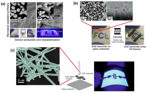
27 Alenezi et al. [81] were able to improve sensitivity, with an ultrafast response time (90 ms) and also a fast recovery time (210 ms). Pimentel et. al. reported a set of studies demonstrating the production of ZnO UV sensors constructed on rigid or flexibles substrates (glass or PET/PEN) and also on cellulosic based substrates [13, 71, 122]. Figure 8 shows ZnO UV sensors produced on cellulosic based substrates and glass.
Figure 8. (a) ZnO UV sensor produced on tracing and Whatman paper [13]; (b) Transparent UV sensor
produced on glass substrate [71]; (c) UV sensor produced with ZnO nanowires on top of graphite electrodes,
screen printed on paper substrate [122]. Reproduced with permission of MDPI [13] and [71], and ACS
publications “Copyright (2018) American Chemical Society” [122].
A disadvantage of using ZnO nanostructures in UV sensing is the low photocurrent value, mainly due the small size of individual nanowires. Some different methodologies are being employed by researches in order to enhance the photoresponse of ZnO UV sensors. Bai et al. [171] showed the difference in using ZnO nanowires aligned horizontally along the substrate or using the same nanowires placed vertically against the substrate. By a transfer process, it was possible to transfer the vertically oriented nanowires into a well aligned horizontal orientation and this way increasing the
28 photoresponse current from 1.8 A to 12.22 mA, with an on/off current ratios of 82000 [171].
One of the most important characteristics that are being studied by scientific community is sensor miniaturization. Portable and small photodetectors have a wide range of applications, such as the monitoring of UV dosage for skin cancer prevention, optical communications and also in astronomy [172]. Nasiri et al. [172] produced small ZnO photodetectors with excellent selectivity and milliampere photocurrents. A spray flame synthesis technique was used (see Figure 9 (a)), producing ZnO nanoparticles with a diameter of 19 nm. The high sensitivity of this sensor is mainly due to the highly pure crystal surface and the very small particle size that originated ultra-porous ZnO nanoparticle film, presenting increased photocurrent from 260 A to 1.2 mA [172].
Another very interesting concept for UV sensor application is presented by Park
et al. [164]. Park was able to produce a wireless UV sensor platform based on ZnO
nanorods where real-time collected signals are sent to a smartphone through Bluetooth connection, with responsivity as high as 0.55 A W-1, response time of 3.1 s and recovery
time of 1.25 s. Figure 9 (b) shows a photograph of the photocurrent measurement by a smartphone.
29 Figure 9. (a) Schematic of a ZnO photodetector production by flame spray pyrolysis [172]; (b)
Photographic image of a ZnO UV sensor Bluetooth-connected to a smartphone [164], where it is visible
the photocurrent variation under on/off cycles of UV radiation. Reproduced with permission of John Wiley
and Sons [172] and Royal Society of Chemistry (2018) [164].
The most recent approach in ZnO UV sensors is the use of graphene as conductive layer to improve their performance [173-175]. The advantage of using graphene relies on its superior conductivity (that prevents recombination of electron-hole pairs in the ZnO/graphene composite) and transmittance (over 97.7 % for a single layer graphene, which maximizes UV-light absorption), allowing a reduction in response and recovery time, and increasing the photocurrent gain [174]. Duan et al. [174] was able to produce a ZnO UV sensor with responsivity of 0.039 A W-1, extremely short response and decay time of 37 s and 330 s, respectively.
Zinc oxide is a biocompatible material, with high isoelectric point (IEPZnO 9.5),
high surface activity and electron communication feature [176, 177]. For these reasons, ZnO can be functionalized with a wide range of biological materials with low IEP values, through electrostatic interaction, such as enzymes (like glucose oxidase and cholesterol
30 oxidase), antibodies or even DNA [176, 178, 179]. Several reports have demonstrated the application of ZnO as biosensors, i.e. in DNA immobilization [180], in glucose level detection [176, 177, 181], for cardiac biomarker detection [179, 182, 183] and also for cancer diagnostic [178, 184, 185].
Probably the application of ZnO for glucose detection is one of the most studied biosensors. For glucose levels detection , ZnO biosensors are produced by immobilization of glucose oxidase enzyme onto ZnO nanostructures [176]. The high IEPZnO value will
promote the formation of zinc oxide/ glucose oxidase complexes during functionalization (glucose oxidase are negatively charged molecules, that will be readily attracted and immobilized onto positively charged zinc oxide).
The detection of glucose by the functionalized electrodes can be described by the following electrochemical reactions: glucose oxidase enzyme oxidizes glucose and as a result -gluconolactone and H2O2 are produced [181]. Finally, with the oxygen
consumption and H2O2 oxidation, it is possible to evaluate the amperometric response of
the biosensor [176, 181]. The use of ZnO nanostructures, with high surface-to-volume, in glucose biosensors, will provide a large specific surface area for glucose oxidase adsorption.
Gallay et al. [176] was able to produce a ZnO nanowire-based glucose sensor capable of detecting very low glucose concentrations of about 9 M. Wahab et al. [181] used ZnO nanorods for the detection of glucose with concentration ranging from 1 M to 10 mM. Wang et al. [177] synthesized ZnO nanocombs, forming a highly porous structure, that were then immobilized with glucose oxidase, showing a detection limit of 0.02 mM.
One of the most key areas of investigation is the development of rapid systems for the diagnostic of cancer. Researchers have found that some biomolecules like DNA
31 molecules, human serum albumin and angiotensin II molecules can be effectively immobilized just by modifying the ZnO nanostructures surface [184]. Viter et al. [178] have demonstrated that by using photoluminescence properties of ZnO nanorods, it was possible to develop a cancer cell recognition system. By immobilization of SSEA-4 antibodies on ZnO nanorods that were then deposited on the cell probe, it was possible to record photoluminescence spectra that increased when compared with the signal of control samples. Moreover, it was possible to observe that the intensity was correlated with the extent of malignancy in target cell population [178]. Another method for the detection of cancer cells was presented by Rui et al. [185]. By adsorbing Cytochrome c (Cyt.c) onto ZnO surface, this latter study used ZnO nanosheets to detect H2O2 from
living cancer cells. Cyt.c was found to promote direct electron transfer at the electrode surface [186].
For cardiovascular disease diagnosis, it was possible to develop a sensor that may detect specific concentration ranges of biomarkers that are associated with those diseases. The presence of cardiac troponin (cTnT and cTnI biomarkers) in blood circulation is an indicative of cardiovascular disease [179, 182]. Shanmugam et al. [182] developed a flexible and disposable electrochemical sensor capable of detecting very low concentrations of target analyte cTnT with only 20 L of solution. The limit of detection was identified at 0.1 ng L-1. Tan et al. [183] produced a biosensor based on ZnO nanoparticles that was capable of converting the biological interaction of cTnI into an electrical signal. This study also detected the cTnI biomarker in a concentration range of 1 ng mL-1 to 10 µg mL-1, withdetection limit of 2.191 ng ml-1 and sensitivity of 15.8 nA (g/mL)-1.
32
2.2 Titanium dioxide
TiO2 is a n-type semiconductor usually appearing in an amorphous state or as three
crystalline phases: the tetragonal phases, anatase and rutile, and an orthorhombic phase, brookite [187]. Rutile is the most stable phase, in which both anatase and brookite are metastable, transforming to rutile when heated [188]. It has been reported that phase transformation of the amorphous state to anatase occurs from 300 to 500 °C, and further transformation to rutile occurs at 600-1000 °C [103, 189].
Rutile and anatase tetragonal structures contain six and twelve atoms per unit cell, respectively. For both phases, each Ti atom is coordinated to six O atoms and each O atom is coordinated to three Ti atoms. The TiO6 octahedron is slightly distorted, with two
Ti-O bonds somewhat greater than the other four, having some of the O-Ti-O bond angles distorted from 90 º (greater distortion in anatase than rutile). The structures of rutile and anatase crystals consist of chains of TiO6 octahedra, sharing four edges in anatase and
two in rutile. In the case of brookite, it has distorted TiO6 octahedra sharing three edges.
Moreover, brookite has eight formula units in the orthorhombic cell, in which the interatomic distances and O-Ti-O bond angles are similar to those of rutile and anatase, nevertheless it has six different Ti-O bonds [190, 191]. Rutile, anatase and brookite unit cells are presented in Figure 10.
33 TiO2 is a wide energy band gap material, typically displaying optical band gaps of 3.0
and 3.2 eV for rutile and anatase, respectively [193], and varying from 3.13 to 3.40 eV [188, 193] for brookite. Nevertheless, its optical bang gap for nanostructured materials can be engineered by adding structural defects or doping with non-metal and metal elements also to narrow its band gap [194-196]. TiO2 has a high refractive index (2.71 for
rutile, 2.53 for anatase and 2.64 for brookite [191]), high dielectric constant (TiO2 thin
films ranging from 40 to 86 [197, 198]) and high resistivity extending to 108 Ω.cm [199]. The lattice parameters for rutile (P42/mnm) are a= 0.4594 nm and c= 0.2958 nm, while
anatase (I41/amd) has lattice parameters of a= 0.3785 nm and c= 0.9515 nm, and brookite
(Pbca) has lattice parameters of a= 0.9184 nm, b= 0.5447 nm, and c= 0.5145 nm [191, 200].
Several techniques have been reported to produce TiO2 nanostructures or thin films
including sol-gel method [201], wet-chemical techniques [202, 203], thermal evaporation [204], sputtering [205], electrodeposition [206], hydrothermal and solvothermal synthesis [207-210], microwave irradiation [10, 192], amongst others. Various and distinct structures have been reported for TiO2 nanomaterials, especially as nanoparticles,
including nanowires, nanorods, nanotubes, nanobelts, nanowhiskers, nanospheres and others [10, 203, 211-213].
TiO2 is known to be an inexpensive material, earth abundant, chemically stable,
non-toxic, biocompatible, and environmentally friendly [203, 214], which makes it prone to be applied in numerous fields, including solar cells [25, 215, 216], self-cleaning [217, 218], photocatalysis [9, 10, 192], H2 production [219], CO2 reduction [220, 221], sensors
[222-224], among others. Anatase is the preferred phase for solar cell integration since it has high electron mobility, low dielectric constant and lower density [225, 226]. TiO2 has
34 splitting, reduction of CO2 to hydrocarbons, and pollutant degradation for many years. In
terms of photocatalytic activity, anatase is expected to exhibit an indirect band gap that is smaller than its direct band gap. Rutile presents a direct band gap or an indirect band gap that is comparable to the direct one. It is known that semiconductors with indirect band gap generally exhibit longer charge carrier life times and thus longer electron-hole pair life would facilitate charge carriers participation in surface reactions [227].Nevertheless, it has been reported that the mixture of both phases displayed higher photocatalytic activity than pure phases [228]. In the case of brookite, this material is the least investigated TiO2 polymorph, however it has been reported to display higher
photocatalytic activity than anatase or rutile [229].
In terms of sensors, and as previously mentioned, a high-quality sensor is expected to have greater sensitivity, high detection limit, response/recovery time and stability and longer life cycles. These parameters are related to characteristics of the sensing material, such as grain size and microstructure, which directly influence the sensor’s sensitivity [199]. In this sense, nanostructured materials have been extensively used in sensors over the years, including nanostructured TiO2 materials that have enhanced chemical stability
allowing low temperature operation. This materials has inert characteristics, and is resistance to harsh atmospheric conditions, despite being low-cost in terms of production and compatible with wet-chemical synthesis routes [230].
TiO2 has been widely used as photoactive layer of gas sensors, where TiO2-based gas
sensors are typically chemiresistive, having the working principle of typical n-type semiconductor gas sensor materials based on its conductance change mechanism due to adsorption/desorption process of oxidizing and reducing gases [231].
Liu et.al. [232] reported the hydrothermal synthesis of TiO2 nanocrystals with various
35 towards ethanol (Figure 11 (a)). In another study, TiO2 nanowire sensors revealed
excellent selectivity and high sensitivity down to 100 ppm NO2 at room temperature with
response and recovery times of 10 s and 19 s, respectively. Furthermore, the nanowires displayed good repeatability and selectivity against various interfering gases such as NH3,
H2, and CH4 [233]. TiO2 nanostructured films composed of different morphologies,
nanoparticles and nanotubes were synthesized by hydrothermal method and it has been shown that sensing films composed of nanotubes demonstrated a high sensor response to toluene [234].
It is also known that well-ordered porous metal oxide structures are highly efficient for improving gas sensing, in which this porosity increases surface area of the material, enhancing its interaction with the gaseous species [231]. TiO2 spongy layers with
double-scale porosity at the meso and nano-double-scale have been reported and exhibited sensitivity of 44 ppm to ethanol at 250 °C. Moreover, response of the material was demonstrated to be independent of ambient humidity with a response time as low as ∼10 s [235].
Another approach that has been widely used is doping with small metal clusters. Doping will have a significant effect for the metal oxides which are dominated by defect chemistry (via oxygen vacancies). Oxygen vacancies are considered important reactive agents for several adsorbates, in such a way that surface reactions are influenced by this type of point defect [49]. Ruiz et al. [236] reported the effect of doping TiO2 with
chromium, in which it has been observed that the addition of Cr retarded the anatase-to-rutile TiO2 transformation, moreover these materials revealed to be sensitive to 1000 ppm
CO, but also to NO2. In another study, it has been described TiO2 sol-gel films doped with
gold nanoparticles used as both optical and conductometric sensors for the detection of CO and H2 [237]. The combination of different oxides has also been reported to surpass
36 nanofiber-structured films that were tested for sensing H2. This combination allowed to
increase TiO2 gas sensitivity and supress SnO2 sensors limitations that utilize
low-temperature chemisorption (under 400 °C) of gases on the surface. Above 400 °C, SnO2 exhibits poor sensing performance, while TiO2 is stable at higher temperatures.
In terms of humidity sensors, TiO2 is known to have superior humidity sensitivity
with the preferably hydrophilic property resulting from the surface defects, i.e. the Ti3+ defect sites or oxygen vacancies sites, that can adsorb water molecules in the atmosphere [239]. Nevertheless, reported TiO2-based humidity sensors usually display
limited sensitivity resultant of low surface/volume ratio, high resistance or poor charge transfer process of single phased TiO2 material. Thus, several approaches have been
designed to overcome these limitations. Ultrathin 2D TiO2 nanosheets with high specific
surface area and surface oxygen vacancy defects have been reported as having ultrahigh humidity sensing performance. These nanostructured sensors revealed significant impedance variation from RH 11% to 95%, short response time (3 s) and recovery time (50 s), as well as small hysteresis ∼ 4.6% (Figure 11 (b)) [239]. Lin et al. [240] reported a humidity sensor based on graphene/TiO2 that at 12-90 %relative humidity , exhibited a
sensing response (S = 151) and humidity hysteresis value of < 0.39 %. In another study, flexible sensors based on TiO2 and conducting polymers have been described. These
humidity sensors demonstrated hysteresis (range of 30–90 % RH) of 2 % RH, with response time of 30 s, and recovery time of 45 s [241]. Doping TiO2 was also considered
for producing enhanced humidity sensors. Zare et al. [242] reported the effect of doping TiO2 with silver in terms of humidity sensitivity, while Buvailo et al. [243] showed TiO2
-based nanomaterial doped with LiCl to produce conducting thin film sensors. The latter sensors were measured in the RH range of 5-95 % and revealed 0.75 and 1 s for sensor response and recovery time, respectively.
37 Recently, TiO2 has been considered as a good alternative for the most common used
UV sensors, i.e. silicon-based sensors [244], as TiO2 is highly photoactive and stable
under UV irradiation due to its band gap [67, 245, 246]. Highly oriented rutile TiO2 nanorod arrays were synthesized by hydrothermal method and tested as UV sensors
achieving a photocurrent of 12.87 μA cm−2 under 365 nm UV light exposure [224]. In another study, anodic TiO2 anatase nanotube arrays were tested as UV sensors showing
high responsivity of 13 A W-1 under λ = 312 nm and fast response with rise time and decay time of 0.5 and 0.7 s, respectively [247]. Epitaxial TiO2 thin films were fabricated
on LaAlO3 single crystal substrates by RF magnetron sputtering, and the sensor exhibited
a maximum photoresponse of 3.63 A W−1 at 310 nm and ultrahigh response speed (∼90
ns)[248]. Nano-branched TiO2 arrays were integrated on self-powered UV sensors. The
photosensitivity increased from 0.03 to 0.22 A W−1 exhibiting excellent spectral selectivity and fast response (0.05 s decay time) [249].
38 Figure 11. (a) SEM images of TiO2 nanosheets together with the response and recovery curves of the
sensors as a function of ethanol concentration [232]. (b) SEM and TEM images of TiO2nanosheets for
humidity sensors together with the transient responding dynamics of the impedance of TiO2
nanosheets-based sensor and calibration curve [239]. (c) SEM images of TiO2 nanowires/PANI/TiO2 nanowires
heterostructured arrays to be used as UV photodetectors together with the time responses of photocurrents
under UV light [250]. (d) SEM and schematic diagram of glucose detection on mesoporous GO/TiO2
nanotubes. The graph showed the current responses with successive injections of glucose [251]. Reproduced
with permission of Elsevier, [232], [239] and [250], and Royal Society of Chemistry (2018) [251].
D. Nunes et al. [246] reported the microwave synthesis TiO2 nanostructured films
grown on bacterial nanocellulose (BNC), tracing paper and polyester film substrates to produce flexible and disposable UV sensors (Figure 12). The UV devices showed responsivities of 0.33 A W-1, 0.16 A W-1 and 0.07 A W-1 for TiO
2 films grown on
BNC, tracing paper and polyester substrates, respectively. The structural characteristics of the TiO2 films and substrates were correlated to differences in the UV photodetection.
39 Figure 12. TiO2 nanostructured films composed by nanorod flower-like structures to be integrated as the
photoactive layer of flexible UV sensors. The films were grown on tracing paper, bacterial nanocellulose and
polyester substrates. The cycling behaviour of the photodetectors at 10 V and under a 360 nm UV source
were investigated. The schematic diagrams of dark and UV irradiation processes are presented. Images
reproduced with permission of Springer Nature (2018) [246].
Another solution proposed to reduce electron-hole recombination is production of metal-doped TiO2 materials. It has been reported that Au nanoparticles deposited on
TiO2 nanotubes showed good wavelength selectivity with high photocurrent as compared
to pure TiO2 devices [252]. The addition of other oxides has also been addressed, for
example in the case of SnO2, it possesses high electron mobility, suggesting a faster
diffusion transport of photon-induced electrons to TiO2 [253]. Chen et al. [253] reported
SnO2-TiO2 nanomace arrays exhibited responsivity of 0. 145 A W-1 at 365 nm, rising time
of 0.037 s, and decay time of 0.015 s. Zu et al. [250] reported a self-powered UV photodetector based on heterostructured arrays of TiO2 nanowires/polyaniline
40 nanoflowers/TiO2 nanowires (Figure 11 (c)). The heterostructure revealed improved
sensing performance when compared to bare TiO2 nanowires.
Metal oxides sensing applications, including in biosensors, is growing fast in recent years. In the case of biosensors, these devices are a rapidly expanding field in analytical chemistry, with an estimated 60 % annual growth rate [254]. This impulse is coming from health-care industry, food quality and safety, but also from environmental monitoring. When comes to using TiO2 in biosensors, several studies have focused on
producing 1D nanostructures forming continuous arrays [223, 251, 255, 256]. The use of TiO2 nanotube/nanorod arrays is related to large internal surface area, negative surface
charge and high refractive index of these arrays allowing incorporation of biomolecules and high analyte sensitivity [223, 255]. Mun et al. [223] reported the production of TiO2
nanotube arrays for label-free optical interferometric biosensing using a protein A capture probe and an immunoglobulin analyte [223]. Mesoporous TiO2 nanotube arrays had
immobilized glucose oxidase (GO) to produce a biosensor for amperometric detection of glucose. The amperometric response of glucose on the GO/TiO2 electrode was reported to be
proportional to glucose concentration in the range from 0.1 to 6 mM with a sensitivity of 0.954 μA mM−1 cm−2 (Figure 11 (d)) [251]. Hu et al. [255] produced carbon-doped TiO
2 nanotube
arrays for simultaneous detection of 5-hydroxytryptamine and ascorbic acid, which can also be readily regenerated photocatalytically to recover its high selectivity and sensitivity. Gao et al. [256] reported a graphene/TiO2 nanorods/chitosan nanocomposite
modified carbon ionic liquid electrode to produce an electrochemical DNA biosensor for detection of the transgenic soybean sequence of MON89788. The target ssDNA sequence was detected in the range from 1.0×10⁻¹² to 1.0×10⁻⁶ mol L-1 with detection limit of 7.21 × 10⁻¹³ mol L-1.
![Figure 1. Scheme of the types of nanostructured materials based on their dimensions: 0D, 1D, 2D and 3D [1]](https://thumb-eu.123doks.com/thumbv2/123dok_br/15449224.1026902/3.892.289.553.732.1024/figure-scheme-types-nanostructured-materials-based-dimensions-d.webp)
![Figure 7. Humidity adsorption models for (a) ZnO nanorods; (b) ZnO/TiO 2 composite nanorods [161]](https://thumb-eu.123doks.com/thumbv2/123dok_br/15449224.1026902/26.892.136.768.229.396/figure-humidity-adsorption-models-zno-nanorods-composite-nanorods.webp)
![Figure 10. Unit cells of TiO 2 rutile, anatase and brookite [192]. Reproduced with permission of Intech.](https://thumb-eu.123doks.com/thumbv2/123dok_br/15449224.1026902/32.892.139.740.867.1077/figure-unit-rutile-anatase-brookite-reproduced-permission-intech.webp)
![Figure 13. SEM images of WO 3 (a) nanoplates produced by microwave hydrothermal method [269]; (b) nanowires produced by thermal evaporation [270]; (c) nanoflowers produced by hydrothermal method [271]; (d) microspheres produced by hydrot](https://thumb-eu.123doks.com/thumbv2/123dok_br/15449224.1026902/42.892.127.766.229.554/nanoplates-microwave-hydrothermal-nanowires-evaporation-nanoflowers-hydrothermal-microspheres.webp)
![Figure 14. (a) Graphene oxide-WO 3 composite nanofibers and dynamic gas sensing curves of the sensors as a function of acetone concentration [279], (b) SEM and TEM image of a Li/K co-doped 3D ordered material to be used as WO 3 humidity](https://thumb-eu.123doks.com/thumbv2/123dok_br/15449224.1026902/50.892.134.753.514.874/figure-graphene-composite-nanofibers-function-concentration-material-humidity.webp)
![Figure 17. Unit cells of cuprous oxide Cu 2 O and cupric oxide CuO [364]. Reproduced with permission of Elsevier (2018)](https://thumb-eu.123doks.com/thumbv2/123dok_br/15449224.1026902/54.892.263.625.896.1083/figure-unit-cells-cuprous-cupric-reproduced-permission-elsevier.webp)
![Figure 20. Unit cells of both SnO 2 [462] and SnO [463]. Reproduced with permission of MDPI [462] and APS Physics (2018) [463].](https://thumb-eu.123doks.com/thumbv2/123dok_br/15449224.1026902/63.892.261.635.919.1080/figure-unit-cells-sno-reproduced-permission-mdpi-physics.webp)
![Figure 21. SEM images of (a-b) nanosheets-assembled SnO 2 hollow spheres for ethanol gas sensor [503], (c) SnO 2 nanoparticles produced at CENIMAT using hydrothermal synthesis, (d) porous flower-shaped SnO 2 nanostructures [504], (e) hie](https://thumb-eu.123doks.com/thumbv2/123dok_br/15449224.1026902/66.892.135.755.231.559/nanosheets-assembled-nanoparticles-produced-cenimat-hydrothermal-synthesis-nanostructures.webp)
