F
ACULDADE DEE
NGENHARIA DAU
NIVERSIDADE DOP
ORTODC/DC Converter with Transparent
Electronics for Application on
Photovoltaic Panels
Romano Jorge de Sousa Torres
Mestrado Integrado em Engenharia Eletrotécnica e de Computadores Supervisor: Vitor Grade Tavares (PhD)
Second supervisor: Pedro Miguel Cândido Barquinha (PhD) Second supervisor: Pydi Ganga Bahubalindruni (MSc)
c
Sumário
A eletrónica transparente é uma tecnologia emergente que pode proporcionar sistemas de baixo custo dada a possibilidade de fabricação de dispositivos a baixa temperatura. A sua aplicação pode ser útil em vários domínios como indumentária eletrónica e sensores de monitorização de saúde. Com a implementação de conversores DC/DC em eletrónica transparente, as aplicações poderiam extender-se para dispositivos com fonte de bateria ou painéis fotovoltáicos.
A tecnologia transparente é baseada em transístores de filme fino (TFT) com semicondutores a-IGZO, material que emergiu nos últimos anos. Os transístores podem ser utilizados para a criação do Conversor DC/DC desejado, o qual pode ser depositado do vidro dos painéis, reduzindo os custos de montagem e conceção de todo o sistema.
Esta dissertação tem como principal objetivo o projeto e desenvolvimento para construção de uma topologia de conversor DC/DC com eletrónica transparente para aplicação em painéis fotovoltáicos. Inclui o estudo de elementos passivos, como bobinas e condensadores, e a sua pos-sibilidade de utilização. A construção e melhoria do conversor DC/DC inclui o desenvolvimento de um regulador para estabilização da tensão de saída.
O trabalho tem a colaboração do grupo CENIMAT da Universidade Nova de Lisboa. Nesse local será construído o conversor DC/DC e os circuitos desenvolvidos nesta dissertação.
Abstract
Transparent electronics is a forthcoming technology, which allows for low-cost systems with de-vices fabricated at low temperatures. Its application may be useful in various domains, such as wearable electronics and sensors for health monitoring. Designing DC/DC converters with trans-parent technology could extend its application to battery operated devices or photovoltaic panels.
Transparent technology, in this work, is based on thin-film transistors (TFT) with a-IGZO semiconductors, material that has emerged in recent years. Their effectiveness for designing DC/DC converters will be assessed. Such converter could eventually be deposited on the glass casing of photovoltaic panels, reducing installation and designing costs of the whole system.
This dissertation has in its main objective the development, design and fabrication of a DC/DC converter topology with transparent electronics, for application in photovoltaic panels. It includes the study of some passive elements, such as inductors and capacitors, and their effectiveness for a possible use. The improvement of the DC/DC converter includes the design of a regulator to stabilize the output signal.
The work is developed in collaboration with the CENIMAT group at UNL, where the devel-oped circuits and DC/DC converter will be fabricated.
Acknowledgments
I would like to thank my family for always support me during this master, to believe in my capa-bility and effort to achieve this important objective in my life.
I thank my friends, Bruno Silva e Henrique Martins, for the support in all the challenges that this master created. All the study meetings before exams were very important to a successful accomplishment of the course.
I would like to thank Bilal Hussain for the help on the inductor simulation and Nuno Cardoso for the development of layout testing files.
I also thank my supervisors, Vitor Tavares, Pedro Barquinha and Ganga Bahubalindruni, for all the help and important discussion regarding the accomplishment of this thesis, the advices and the development of TFT simulation model.
Romano Jorge de Sousa Torres
Contents
1 Introduction 1
1.1 The World of TFTs and Motivation . . . 1
1.2 Generic Proposed Solution . . . 2
1.3 Structure of the Document . . . 3
2 Background 5 2.1 Transparent electronic devices . . . 5
2.1.1 Resistors . . . 5 2.1.2 Capacitors . . . 6 2.1.3 Inductors . . . 7 2.1.4 Thin-film transistors (TFT) . . . 7 2.1.5 Fabrication processes . . . 13 2.2 Voltage Multipliers . . . 14
2.2.1 Output Voltage and Load Current . . . 14
2.2.2 Power and Efficiency . . . 17
2.2.3 Step-Up and Step-Down - a question of design . . . 19
2.3 Operational Amplifiers with transparent TFT’s . . . 21
2.3.1 Single-Stage Amplifiers . . . 22
2.3.2 Differential Pair . . . 25
2.3.3 Multi-Stage Amplifiers . . . 27
3 Bibliographic Review 29 3.1 Thin-Film Transistors using a-IGZO . . . 29
3.2 Charge-Pumps . . . 31 3.2.1 Non-transparent designs . . . 31 3.2.2 Configurations with TFT’s . . . 33 3.3 Regulators . . . 37 3.3.1 Linear Regulation . . . 37 3.3.2 Pulse-Width Modulation . . . 39 3.4 Critical Analysis . . . 40
3.5 Conclusion for the Proposal . . . 41
4 Proposed Configuration 43 4.1 DC/DC converter . . . 44 4.1.1 Design . . . 44 4.1.2 Simulation . . . 48 4.2 Amplifier . . . 50 4.2.1 Design . . . 50 ix
x CONTENTS
4.2.2 Simulation . . . 54
4.3 Regulator . . . 56
5 Conclusions and Future Work 61
List of Figures
2.1 Transparent resistor from a planar view [1] . . . 5
2.2 Transparent resistor from cross-sectional view [1] . . . 6
2.3 Transparent capacitor from plan view [1] . . . 6
2.4 Transparent capacitor from cross-sectional view [1] . . . 6
2.5 Bottom-gate TFT Device Structures . . . 8
2.6 Top-gate TFT Device Structures . . . 8
2.7 Transparent TFT in cut-off mode (no current flow) . . . 9
2.8 Transparent TFT in linear mode . . . 9
2.9 Transparent TFT in saturation mode . . . 10
2.10 Switch mode transistor with capacitor at the drain [2] . . . 11
2.11 Switch mode transistor with capacitor at the source [2] . . . 12
2.12 Cockcroft-Walton configuration [3] . . . 14
2.13 Dickson charge pump [4] . . . 15
2.14 Voltage doubler [5] . . . 18
2.15 Simply cascade voltage doublers [5] . . . 18
2.16 Multiphase voltage doublers [5] . . . 18
2.17 Dickson charge pump [5] . . . 18
2.18 Charge-Pump Step-Up Converter [6] . . . 19
2.19 Charge-Pump Step-Down Converter [6] . . . 20
2.20 Common-source stage . . . 22
2.21 Common-source stage with source degeneration . . . 23
2.22 Source-follower stage . . . 23
2.23 Common-gate stage . . . 24
2.24 Cascode stage . . . 25
2.25 Differential pair . . . 25
2.26 Application of Miller effect to a floating impedance . . . 27
2.27 Common-source stage with parasitic capacitances . . . 28
3.1 Cross-connected configuration from P. Favrat et al. [7] . . . 32
3.2 Bootstrapping configuration of charge-pump from Allasasmeh and Gregori [8] . . 32
3.3 Switched Capacitor based Buck Converter [9] . . . 33
3.4 Transparent Step-Up DC/DC Converter [10] . . . 34
3.5 Dickson charge-pump [10] . . . 34
3.6 Cross-coupled DC/DC converter [10] . . . 35
3.7 Transparent step-down DC/DC converter [10] . . . 35
3.8 DC/DC converter design in organic technology [11] . . . 36
3.9 Proposal of linear regulator from Bhattacharyya et al.. Image obtained in [12] . . 37
3.10 Schematic of regulation from Bhattacharyya et al. [12]. Image obtained from [12] 38
xii LIST OF FIGURES
3.11 Proposal of linear regulator from B. Maity et al. [13]. Image obtained from [13] . 38
3.12 Schematic diagram of regulation from B. Maity et al. [13]. Image obtained from
[13] . . . 38
3.13 Schematic diagram of regulation with inverter from B. Maity et al. [14]. Image obtained from [14] . . . 39
3.14 Configuration of charge-pump with PWM regulation proposed by Y. Chang [15]. Image obtained from [15] . . . 40
4.1 Inductance response depending of frequency . . . 44
4.2 Quality factor depending of frequency . . . 44
4.3 Proposal of DC/DC converter . . . 45
4.4 Designed layout of the single DC/DC converter . . . 47
4.5 Output voltage of the single DC/DC converter during the time . . . 49
4.6 Comparison of output voltage during the time with and without bootstrapping stage 49 4.7 Output voltage of 10 DC/DC converter in parallel during the time . . . 50
4.8 Proposal of regulator . . . 51
4.9 Designed layout of the proposed regulator amplifier . . . 55
4.10 Voltage gain of the amplifier for a logarithmic frequency scale . . . 55
4.11 Phase response of the amplifier for a logarithmic frequency scale . . . 55
4.12 Final circuit . . . 56
4.13 Voltage level during the time for different nodes of the circuit . . . 57
4.14 Results for the simulation with voltage source . . . 58
List of Tables
3.1 Simulated results of negative DC/DC converters with load current . . . 35
4.1 Parameters of the inductor simulated . . . 43
4.2 Sizing of the capacitors for the proposed DC/DC converter . . . 46
4.3 Area of each capacitor designed . . . 48
4.4 Output voltage and current for different values of load resistance for the proposed DC/DC converter . . . 49
4.5 Dimensions of TFT for the feedback stage . . . 52
4.6 Dimensions of TFT for the differential pair . . . 52
4.7 Dimensions of TFT for the source-follower stages . . . 53
4.8 Dimensions of TFT for the common-source stages . . . 53
4.9 Voltage gain for each stage of the amplifier . . . 56
4.10 Voltage level for each node of the circuit . . . 58
Abreviaturas e Símbolos
a-IGZO amorphous Indium Gallium Zinc Oxide DC Direct currentFEUP Faculdade de Engenharia da Universidade do Porto ITO Indium Tin Oxide
LCD Liquid-Crystal Display LPF Low-Pass Filter
MPDV Multiphase voltage doubler PWM Pulse-Width Modulation PCB Printed Circuit Board TFT Thin-Film Transistor TPVD Two-phase voltage doubler UNL Universidade Nova de Lisboa UV Ultra-violet
Chapter 1
Introduction
1.1
The World of TFTs and Motivation
The industry of integrated circuits design is always searching new ways to improve the perfor-mance of the electronic devices. During the last century, electronic technology has emerged in such scale, appearing more and more devices that change the global life style and push the human-ity towards new targets previously unreachable.
Thin Film Transistors are electronic devices that have been studied in recent years due to their low-cost fabrication, which can decrease the cost of application in various domains such as military, radio-frequency, sensors in health monitoring, wearable electronics and much more. The most common application of TFT is the liquid-crystal display technology (LCD). In this situation, TFT can reduce the crosstalk between the pixels, providing a better control of each pixel and improving the image quality in displays.
TFT’s are field effect type, and are structurally built from deposition of thin-films on a non-conductive substrate, like glass or ceramic, which have good electrical isolation properties and reduce the parasitic capacitance comparing with monolithic circuits. A semiconductor layer and a dielectric layer are deposited between two metal contacts that represent the source and drain. Besides the improvement of this technology, transparent conducting oxides have been tested to use in TFT’s, in order to create full transparent electronic devices. One of the most used material in recent years is the amorphous Indium Gallium Zinc Oxide (a-IGZO), which various reports suggest a better performance when compared to Zinc Oxide (ZnO).
The main focus of this thesis is the study and implementation of DC/DC converters with transparent electronics. The possibility of fabrication processes at low temperature allows the development of TFT on flexible substrates at an evermore low cost. The transparent DC/DC converters could be used on photovoltaic panels by deposition on glass substrate, possibly raising its cost effectiveness.
Today, there are many studies concerning climate changes that result from the burning of non-renewable energy sources, causing emissions of carbon dioxide to atmosphere and developing greenhouse effect. Due to an increasing world population, the energy demand rises, depleting
2 Introduction
petroleum and other non-renewable energy sources. The research on alternative and renewable energy sources is then of outmost importance. Photovoltaic energy is one possibility.
Photovoltaic panels often use DC/DC Converters. They are mainly electronic circuits that change the voltage value from input to output, working with direct currents (DC). Their application extend to battery supplied devices, like mobile phones, laptops, typically to increase the voltage provided. Converters are used also on photovoltaic panels. In this case, the converter produces a regulated output voltage from energy temporarily saved, releasing it on a different voltage value, with increasing efficiency.
Now-a-days, the inclusion of photovoltaic panels on daily life is possible, by either using the roofs of buildings or large fields, but the creation of transparent devices can be considered as a possibility of embodying the electronics with panels. Such approach could effectively down-size the overall cost of the electronics (low-temperature fabrication) and of assembly (deposition of electronic system on the glass casing). This is the main motivation behind the present proposal for dissertation.
1.2
Generic Proposed Solution
The most common DC/DC Converters use inductors as a passive element to store energy, to in-crease or dein-crease the voltage level at the output. Due to the fact that transparent materials have lower conductance than metals, there is a large parasitic resistance associated to them. The cre-ation of a high performance inductor, where the coil needed for magnetic field forces it to have a long path, is expected to be a challenging task. The longer the path is, lower is the quality factor of the inductor. To overcome this problem, other different electronic topologies can be used to increase an input voltage with DC current, such as charge pumps and voltage doublers. These devices have the same purpose as the standard ones, but due to their non-inductive behaviour, they can have more undesirable drawbacks. One of them is the increased voltage ripple, that reduce the precision of voltage level at the output.
Another limitation is the lack of p-type devices, due to the undesirable levels of carrier concen-tration, mobility and band-gap that this type of transparent materials have. Only n-type transistors can be used in transparent circuits designed, that forces to a different implementation of the cir-cuits.
The lack of investigation in this field is another limitation. The most common studies of transparent electronics are focused on TFT parameters, which the first report is from Nomura et al. in 2004 [16]. Therefore, new electronic topologies will be needed for the design of a DC/DC converter with transparent electronics.
The proposal described in this report, for a positive DC/DC converter topology to be imple-mented with transparent electronics, uses switched-capacitor concepts to circumvent the need for inductive elements. However, there are other issues that need to be taking into account. In chapter
4is presented the proposal of DC/DC converter and a method to regulate the output voltage, with the study of the respective parameters and behaviours that results from that design.
1.3 Structure of the Document 3
1.3
Structure of the Document
Besides the introduction, this report has 4 more chapters.
Chapter 2discusses the fundamentals and theory behind the construction of DC/DC converters with transparent electronics and their regulation.
Chapter 3presents the state of the art, where various studies, closely related to the goal of this dissertation, are exposed.
Chapter 4 presents the schematic and the layout of the final proposal for the transparent DC/DC converter and the regulation method, with a deep study of the results obtained with the circuit designed.
Chapter 5presents the conclusions and the future work that can be made regarding DC/DC converters with this technology.
Chapter 2
Background
2.1
Transparent electronic devices
Standard DC/DC converters use various components such as resistors, capacitors, diodes and in-ductors. Regarding the goal of designing such device with transparent electronics, a study about transparency and its effect on the behaviour of passive devices is very important, to analyse how worth is the usage of each component.
To create transparent devices, different materials should be combined to perform the same functions of non-transparent devices. The efficiency of new devices created should be, as possible, equal or better to the existing ones. However, the characteristics of transparent electronic materials comparing with the others, like smaller conductivity, decrease their efficiency.
There have been many studies to create high performance devices. They focus on the layout of materials, and the results are sometimes very different from what could be expected with non-transparency.
2.1.1 Resistors
A good performance resistor should fulfil the characteristic defined by Ohm’s law; it should have a linear behaviour according to this law. Parasitic capacitance is undesirable, therefore those should be fabricated on insulating substrates.
Taking advantage of the smaller conductivity of transparent materials, resistors are created with a long path between two contacts. The layout can be seen in figures2.1and2.2.
Figure 2.1: Transparent resistor from a planar view [1]
6 Background
Figure 2.2: Transparent resistor from cross-sectional view [1]
The passivation layer is created to protect the resistor physically and chemically. The resis-tance value depends of the parameters from the equation:
R=ρ L
W t (2.1)
where ρ is the resistivity of the material, L is the path length, W is the path width and t is the path thickness. The resistance value is proportional to the resistivity of material and the path length. It is inversely proportional to the width and the thickness. To reduce the area of the resistor and obtain the maximum resistance, a rectangular zigzag shape is normally adopted along the resistor length2.1.
2.1.2 Capacitors
Capacitors should have a linear current-voltage derivative characteristic. They are created to store energy in an electric field form. A transparent capacitor can be achieved with a transparent electric insulator between two contacts. The layout can be seen in figures2.3and2.4.
Figure 2.3: Transparent capacitor from plan view [1]
2.1 Transparent electronic devices 7
The capacitance value depends of the parameters from the equation:
C=ε LW
d (2.2)
where ε is the insulator dielectric constant, L is the length and W is the width of the overlapping area, and d is the dielectric thickness. The capacitance is proportional to the insulator dielectric constant and the plates area. It is inversely proportional to the insulator thickness.
2.1.3 Inductors
Inductors store energy in a magnetic field, but due to poor conductance and consequently high par-asitic resistance of transparent materials, it is difficult to create these devices with linear voltage-current derivative as expected.
In fact, the resistance related to the transparent material is so high, that the large number of turns needed for inductor increases the length of material and consequently the parasitic resistance [1]. With high parasitic resistance, the quality factor of inductor will be low. Therefore, other ways to create DC/DC converters need to be studied. One possible solution can be voltage multipliers, referred in the next section.
2.1.4 Thin-film transistors (TFT)
TFT’s use the principle of insulated-gate field-effect, which work with similar principals of the MOSFET transitor. The differences between the two devices are the properties of the materials, their fabrication and the smaller thickness of the semiconductor. In fact, the TFT’s are fabricated on the top of an insulating substrate, as opposed to MOSFET technology, that uses the semicon-ductor as substrate. This difference reduces the parasitic capacitance associated to diffusions that occur in monolithic circuits.
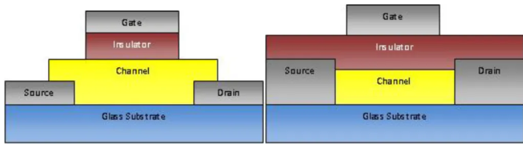
The basic function of these devices is to control the current between drain and source with an input voltage at the gate (to the source). Due to their characteristics, transistors can be used as a switch or even as a diode. The ability to set the device in multiple operation modes makes them the core of electronics. Different structures of the device are possible and various technological parameters can change their characteristics. There are four different structures of TFTs studied, the staggered bottom-gate, staggered top-gate, co-planar bottom-gate and co-planar top-gate struc-tures. The different layouts can be observed in figures2.5and2.6.
Classification differs with the relative positions of the channel (semiconductor), insulator, gate, source and drain. If the contacts are at the same level as the channel, it is a co-planar structure, otherwise it is staggered. The designation of top-gate and bottom-gate differs on the gate position as the name suggests.
8 Background
(a) Staggered bottom-gate structure (b) Co-planar bottom-gate structure
Figure 2.5: Bottom-gate TFT Device Structures
(a) Staggered top-gate structure (b) Co-planar top-gate structure
Figure 2.6: Top-gate TFT Device Structures
2.1.4.1 Materials used for transparent TFT
Research have been made during the years for the creation of transparent TFTs. Results have been more successful with n-type semiconductors. There are no solutions yet about high performance p-type transistors, because the mobility, carrier concentrations, and band gaps of this type of semi-conductors are not reliable to realize [1]. Therefore, the materials presented for channel layer are typically solely n-type, and transparent circuits have to take into account this limitation.
The first transparent thin-film transistors created were reported in 2003 [17] [18] [19]. They used a ZnO channel layer in a staggered bottom-gate structure. Improvements have been made, and K. Nomura [16] in 2004 presented a transparent TFT using amorphous Indium-Gallium-Zinc Oxide (a-IGZO) with mobility exceeding 10cm2/V.s.
Gate dielectrics are very important because it impacts on the number of interface states, should show high dielectric constant and low leakage current. Al2O3, Y2O3and Sc2O3 are materials that
present good performance as dielectric [1]. Drain-source contacts should have low resistance. P.Barquinha et al. [20] suggests the usage of molybdenum (Mo) or Ti/Au contacts due to their good characteristics.
2.1.4.2 Transparent TFT ideal operation mode
Transparent TFT ideal behaviour is very similar to the common MOSFET. The difference between gate and source voltage, VGSvalue, determines the mode in which the TFT is operating. With the
2.1 Transparent electronic devices 9
VGSis smaller than a threshold voltage Vth, there is no current through the channel and transistor
is in cut-off mode. This mode can be seen in figure2.7. The formula of current in this operation mode is:
IDS= 0 (2.3)
Figure 2.7: Transparent TFT in cut-off mode (no current flow)
If VGS is greater than Vth, an uniform electron accumulation layer at the interface
channel-insulator is formed, and current can flow from the source to the drain. When the VGS value
in-creases, the electron layer and the current flow increases. This is the pre-saturation mode. This mode can be seen in figure2.8. The formula for the current in this operation mode is [1]:
IDS=
W
LµCG[(VGS−Vth)VDS− VDS2
2 ] (2.4)
Figure 2.8: Transparent TFT in linear mode
where W is the gate width (µm), L is the gate length (µm), µ is the channel mobility (cm2/V.s), CGis the gate capacitance density (F/cm2), VGS is the gate-source voltage (V), Vth is threshold
voltage (V) and VDSis drain-source voltage (V).
The current value does not increase to infinite with bigger VGS. There is a maximum value,
called saturation current, where the current stabilizes despite an increasing VDS. This mode can
be seen in figure2.9, where it is visible a depletion of electrons near the drain. The effect of the channel modulation, due to the decreased channel length with high drain voltage, can also increase the current by a λ parameter. The formula of current in this operation mode is:
IDS=
W
2LµCG(VGS−Vth)
2(1 + λV
10 Background
Figure 2.9: Transparent TFT in saturation mode
2.1.4.3 Transparent TFT non-ideal characteristics
The material used for transparent TFT present worse characteristics, and causes more detrimental behaviour than MOSFET’s counterparts. The main issues are threshold voltage shift and source-drain contact resistance.
The main cause for threshold voltage shift is the charge trapping in the channel-dielectric interface. A. Suresh and J. Muth [21] report the occurrence of positive gate bias stress due to negative charge trapped between these two layers, resulting on smaller current flowing through the channel. Therefore, larger gate-source voltage is needed to overcome the reduction of free carriers in the channel.
Some reports [22] [23] rises concern on the instability of threshold voltage with water vapour exposure and describe the effects of environment conditions on the TFT operation and character-istic. Under positive gate voltage stress, oxygen is absorbed on IGZO, capturing an electron from the conduction band and decreasing the accumulated electrons density, thus increasing threshold voltage. However, water vapour exposure gives an electron, decreasing threshold voltage value.
Different proposals have been reported to improve this behaviour. Annealing of channel layer makes a better performance in this characteristic, resulting on more stable threshold voltage [16]. Passivation also avoids a large influence of atmospheric conditions, protecting the channel with a diffusion barrier layer and decreasing the threshold voltage shift [23].
Some studies are also concerned with the effects of temperature and light on threshold voltage shift, which is very important to refer due to the specific application in question — photovoltaic panels. S. Kuk et al. [24] report an increase from 0.89 V to 4.35 V as light temperature increases from 30oC to 90oC, explaining the donation of electrons to the conduction band as reason for so large increase. Light illumination enhances the charge trapping.
S. Lee et al. [25] refer a threshold voltage shift in 7000 seconds by less than 1 V in dark state, but an 8.7 V shift with 400 nm light and intensity of 0.025mW /cm2, when a negative bias stress is applied. However, they also report a saturation value for the shift, caused by the filling of the available charge-trapping states to the full.
Threshold voltage shift is an increasing problem if the transistor is conducting for a long time. DC/DC converters use clock signals to open or close the transistor as a switch, so the transistor will not have a large time of conduction and threshold voltage shift will not be the main problem to concern. However, for the regulation of the output voltage of the DC/DC converters, it is necessary
2.1 Transparent electronic devices 11
to create an amplifier that requires specific values of threshold voltage for its TFT’s, otherwise it is unstable. For this reason, this is an issue that concerns more when the regulator is designed.
Another possible reason of concern with TFTs is the source-drain contact resistance. Accord-ing to P. Barquinha et al. [20], source-drain contact resistance is a phenomenon that affects the performance of thin-film transistor, mainly the mobility of short channel devices, because the over-lap between contacts and the channel may not be negligible when compared to the length of the channel. They report higher maximum current in linear and saturation modes with molybdenum (Mo) or Ti/Au contacts. They also refer an improvement on maximum current and field-effect mobility with annealing after placing source-drain contacts. Source-drain contact resistance can decrease the current flowing through a closed transistor, creating a voltage drop. For a boost converter, a high voltage drop can result in a low voltage level at the output.
2.1.4.4 Transparent TFT as a switch
In order to use transparent TFT to implement a switch, it is important to study the behaviour of the transistors in this situation. Speed and voltage precision are issues that should be referred in detail.
B. Razavi [2] studied the behaviour of the transistor as a switch with a circuit described in figure2.10. Ch Vin=0 CLK T1 Vout Vdd +
-Figure 2.10: Switch mode transistor with capacitor at the drain [2]
Suppose that the drain of the transistor is connected to a charged capacitor with an initial voltage of VDD. If CLK = VDDat initial time, the transistor operates in saturation and the capacitor
is discharged, decreasing the value of Vout. When Vout= VDD− Vth, the transistor operates at the
triode region. The capacitor continues to discharge until zero voltage. In the case of figure2.11, where the capacitor is connected to the source, Vincharges the capacitor when CLK = VDD.
If the gate has a voltage level of VDD, the transistors conducts current in both directions to have
the same voltage at both sides. The author determines the output voltage level depending on time (t) as: Vout= VDD−Vth− 1 1 2µ CG CHt+ 1 VDD−Vth (2.6) Analysing this formula, it can be assumed that the voltage at the output will never be higher than VDD−Vth, and the lower mobility of the transistor can decrease this voltage to very low values.
12 Background Ch CLK T1 Vout + -0 Vin=Vdd
Figure 2.11: Switch mode transistor with capacitor at the source [2]
That suggests the effect of on-resistance will have a large effect on the output voltage level. The on-resistance can be determined by:
Ron=
1
µCGWL(VDD−Vin−Vth)
(2.7) The input voltage has also an effect on this resistance, increasing it if the voltage level is higher. Another consideration to take into account is the speed. The factors that influence the time response is the on-resistance of the transistor and the capacitance used. Those create a time constant τ = RonCHassociated, that increases as higher the value of resistance and capacitance is.
Due to the effect of the input voltage on the on-resistance, the voltage level can increase the time constant as well. One common problem associated to the utilization of a transistor as a switch and its effect on precision is the charge that is accumulated in its channel during the on-time. This charge can be calculated as:
Qch= W LCG(VDD−Vin−Vth) (2.8)
When the transistor turns off, this charge exits from drain and source, half for each other, giving some current that should not exist. This phenomenon is called charge injection and creates an undesired ripple, DC offsets and non-linearity if the body-effect is taken into account. The voltage error level associated to charge injection on each side is calculated by:
∆V =W LCG CH
(VDD−Vin−Vth) (2.9)
Another consideration for voltage precision is the clock feedthrough, which results from par-asitic capacitances coupling between gate-source and gate-drain. Considering Cov the overlap
capacitance per unit width, the error can be expressed as:
∆V = VCLK
WCov
WCov+CH
(2.10) Analysing carefully the formulas of speed (time constant) and voltage precision associated to charge injection, it can be concluded that there is a trade-off on choosing the value of the sampling capacitor and the width of transistors. If the transistors are larger, it reduces the on-resistance and
2.1 Transparent electronic devices 13
improves the speed, but it increases the error level. If the sampling capacitor is larger, it reduces the speed and also the error level. Notice that the mobility and length of the transistor do not influence the voltage, and the input voltage does not influence the clock feedthrough unlike the voltage level at the gate.
2.1.5 Fabrication processes
Since the appearance of transparent thin-film transistors that research is made to improve the fabrication processes. The goal is to achieve more precision and control of thickness and layout, when the thin-film is created. The fabrication processes of transparent devices include pulsed laser deposition, photolithography, etching, chemical layer deposition, atomic layer deposition and physical vapour deposition.
2.1.5.1 Pulsed laser deposition
K. Nomura et al. [16] report this technique in the first TFT created. It is used for deposition of indium gallium zinc oxide (IGZO) and indium tin oxide (ITO) thin films. Inside a vacuum chamber, a high and short energy laser pulses collide on a solid target, typically ceramic. The laser pulse beam creates a phenomenon of vaporization of the target. The vapour condenses, and generates a thin film on the substrate.
2.1.5.2 Photolithography
It is the process of transferring images from the computer database to the wafer. Initially, it is used a computer-aided design system to draw the layer. Then, a photoresist is exposed to ultraviolet light, which make its material characteristics to be altered. A photomask is used to create the pattern where it is opaque or transparent to UV light.
2.1.5.3 Etching
This process removes the exposed material created on photolithography to refine the desired pat-tern. This can be achieved by wet etching, where acids are used to remove the material depending on the time and temperature it is exposed, and dry etching, where the material is exposed to a bombardment of ions, and portions of material are removed selectively.
2.1.5.4 Chemical layer deposition
Technique obtained by the introduction of chemical gases on a chamber, which reacts with the wafer in order to design the thin film. This makes a flow system, where reactant gases flow into the substrate and products are removed from it.
14 Background
2.1.5.5 Atomic layer deposition
The thin-film layers are obtained from a sequential exposure of precursors, or chemical gases, reacting with the substrate. It is a self-limiting process, which enables a control on growth depo-sition and uniformity even on large areas, and it differentiates from chemical layer depodepo-sition due to the separation of precursors by inert gas during reaction.
2.1.5.6 Physical vapour deposition
These processes create deposition of atoms from a source onto a substrate. The two mainly pro-cesses of this type are evaporation and sputtering. In the first, it is created by a resistive heating with electric current. While the material is melting and evaporating, the vapour material con-denses, creating the thin film. The second one, sputtering, uses the collision of gaseous ions to dislodge atoms while thin film is deposited. It is a very controllable technique in terms of thickness of the film, and very used nowadays. CENIMAT, a Portuguese scientific research centre, uses the RF sputtering technique [26]. It utilizes energy from radio waves to ionize the gas atoms. Further, the ions get in contact with the substrate, creating the film.
2.2
Voltage Multipliers
Voltage multipliers or charge-pumps use capacitors and switches or diodes to achieve a different output voltage. The principle of operation is to store energy in capacitors, charging and discharg-ing, transferring it to the output load [5]. The study of these devices can be important for the implementation of transparent DC/DC converter, because it could enable the desired functionali-ties of a normal DC/DC converter without using inductors, avoiding the problems referred to the construction of a transparent inductor, such as the low quality factor.
2.2.1 Output Voltage and Load Current
In order to build a background on specific parameters, behaviour of the charge-pumps and to understand the principles of functioning that exist in these devices, some of the initial charge-pump topologies created will be presented. The first voltage boosting circuit designed was the Cockcroft-Walton [3], presented in figure2.12.
Vin CLK2 CLK1 C C C C C C C Cs Cs Cs Cs Cs Cs Cs Cs Vout Cs
2.2 Voltage Multipliers 15
This circuit uses n-stage diodes connected to coupling capacitors that are charged by the clock signals with the same voltage level as Vin, and provide this charge to the output stage. With N
stages, the output voltage expected would be (N + 1)Vin if the non-ideal characteristics are not
taken into account.
In a way of improving, J. Dickson [4] modified the circuit, connecting each of the coupling capacitors directly to the clock inputs, designing the capacitors in parallel. The circuit is presented in figure2.13. C C C C Cs Cs Cs Cs Vin CLK1 CLK2 Vout
Figure 2.13: Dickson charge pump [4]
The increased voltage in each stage is given by:
VN−Vin= VC−VD−VL (2.11)
where VC is the voltage level due to the coupling capacitors, given by the ratio VC =C+CC SVCLK,
VDis the voltage drop in each diode and VLis the voltage that the capacitors charge and discharge
with a load current at the output given by Iout = f (C + CS)VL(f is the clock frequency). The final
expression for N stages is given by:
VN−Vin= N[( C C+CS )VCLK−VD− Iout (C +CS) f ] (2.12)
The maximum output resistance of a charge-pump with N stages depends of the frequency and the pumping capacitors by:
Rout=
N f CCLK
(2.13) An important theoretical analysis of the charge-pumps is made by R. Perigny [27]. This author calculates the output voltage level of one stage of a charge-pump with an inclusion of ripple maximum and minimum level. In the load capacitor, the charge Qload accumulated when the
lower voltage Vlowis applied to the terminals is:
16 Background
When the boosting capacitor Cais charged to VDD, the charge is expressed as:
Qa= CaVDD (2.15)
When Caconnects to Cload, it is applied the voltage Vhigh, and the charge at the load Qload2is:
Qload2= CloadVhigh (2.16)
At this time, the charge stored in the boosting capacitor is:
Qa2= Ca(Vhigh−VDD (2.17)
The principle of conservation requires that:
Qa+ Qload= Qa2+ Qload2 (2.18)
The slope at the output is given by Iout/(Cload+Ca, and it decreases in half clock period, so:
Vhigh= Vlow+
Iout
2 fclk(Ca+Cload
(2.19) Combining the two equations and simplifying, the lower voltage is given by:
Vlow= 2VDD−
Iout
2 fclkCa
(2.20) With no load current, the output voltage is estimated by 2VDD, but this level changes when it
is applied a load resistance at the output, creating a load current. Therefore, there is a decrease of Io/Ca on the output voltage, where Ca is the pumping capacitance, so the voltage difference
between maximum and minimum, with a clock frequency of fclk, is:
∆Vout=
Io
2 fclkCa
(2.21) If a load capacitor Cxis added to the output, the voltage ripple is not so large, due to the slower
transition of voltage level. The slope can be calculated by:
∆Vout=
Io
2 fclk(Ca+Cx)
(2.22) With the voltage ripple calculated, the minimum voltage level is the difference between 2VDD
and ∆Vout without the load capacitor. Notice that the load capacitor is used only to reduce the
maximum voltage Vhigh, and it does not have influence on the Vlow. The maximum voltage is:
Vhigh= Vlow+ Io 2 fclk(Ca+Cx) = 2VDD− Io 2 fclk(Ca+Cx) + Io 2 fclk(Ca+Cx) (2.23)
2.2 Voltage Multipliers 17
This expression does not take into account the on-resistance of the diodes, that reduce the output voltage as higher as the resistance is. In chapter 3will be presented and discussed newer and improved topologies, which reduce some constrains that exist in these circuits.
2.2.2 Power and Efficiency
Efficiency is an important parameter to study when DC/DC converters and charge-pumps are de-signed. D. Baderna et al. [28] calculate the efficiency by the relation between the power at input and output. The power at the input is equal to the sum of power at the output, added by the resistive and dynamic losses, so the efficiency is:
η = VoutIout VoutIout+ Pres+ Pdyn
= VoutIout
VoutIout+ Rout,idIout2 + kN f CparVDD2
(2.24) where k is a coefficient of proportionality and Cparis the equivalent parasitic capacitance in each
stage. The author divides the parasitic capacitance in two parts, Ctopand Cbot. The first component
is more dependent of the topology, because it is created by the design of wider transistors and the voltage level that the transistors have in their terminals. If C represents the value of the pumping capacitors in each stage, the output voltage of the both devices can be calculated as:
Vout=
C C+Ctop
[(N + 1 + β )VDD− Rout,idIout] (2.25)
The effective output resistance is Rout=C+CC
topRout,id, and the maximum load current that the
devices can deliver is Iout,max=RNVout,idDD = f CVDD, so the efficiency can be estimated as:
η = VDDIout(N + 1 + β − Rout,idI
2 out
VDDIout(N + 1 + β ) + (α + β )(1 + β )N f CVDD2
(2.26) The conclusion is that the efficiency η decreases as higher as β is.
J. Starzyk [5] compare different charge-pump designs on the boosting energy required. Since the load resistance is not infinite, the circuits do not present a perfect behaviour, such as Vout/Vin=
0.5 in step-down and Vout/Vin= 2 in step-up converter. The output voltage is as lower as the load
resistance is.
The author [5] present a two-phase voltage doubler (TPVD) with the design in figure2.14. The doublers can be used in cascade as represented in figure2.15.
Removing the second capacitor in each doubler, J. Starzyk [5] presents a multiphase voltage doubler (MPVD), which need half of the capacitors for the same output/input voltage ratio. The circuit is shown in figure2.16.
Starzyk compares the improved charge-pumps to the standard one from Dickson in figure2.17. Some of the Starzyk’s conclusions [5] are that the number of stages used does not affect the output power. It depends on the load resistance, capacitors and clock frequency. When the value
18 Background Vin Vss CL Vo 2 1 2 1 C1 +
-Figure 2.14: Voltage doubler [5]
Vin Vss 2 1 2 1 C1 + -Vss C2 C4 2 1 1 2 C3 Vss CL C2n-1 2 1 1 2 RL Vo
Figure 2.15: Simply cascade voltage doublers [5]
Vin Vss 2 1 2 1 C1 + -Vss C2 Vss CL RL Vo 4 3 3 4 Cn 2n 2n-1 2n-1 2n
Figure 2.16: Multiphase voltage doublers [5]
Vin 1 2 Vo CL C C C C C C C
Figure 2.17: Dickson charge pump [5]
2.2 Voltage Multipliers 19
charge pump as:
WD=
(N + 1)(N + 2)
12 AV
2
in (2.27)
where A is the designed area with equal capacitors and N is the ratio Vout/Vin. The TPVD’s
topology has a boosting energy of:
Wt p=
5(N2− 1)A 12log2N
Vin2 (2.28)
and for MPVD’s topology:
Wmp=
(4N2− 1)A 6log2N
Vin2 (2.29)
The results show that for TPVD’s and MPVD’s energy depends less than quadratically with voltage gain [5]. For Dickson’s charge pump, the dependency is higher. In fact, the output power for the same load resistance is higher on Dickson’s charge pump and lower on TPVD’s. TPVD’s presents also lower rise times than MPVD’s.
2.2.3 Step-Up and Step-Down - a question of design
M. Wens and M. Steyaert [6] presented another example of charge-pump step-up DC-DC con-verter based on charge-pump, as shown in figure2.18, studying its output voltage level and effi-ciency expected. + − S1 S2 S2 S1 C1 C2 Vin RL Vo +
-Figure 2.18: Charge-Pump Step-Up Converter [6]
When the switches are at position 1, the voltage source charges capacitor C1. CL discharges
to RL. When the switches are at position 2, the lower terminal of C1 connects in series with the
voltage source, and CLand RLreceive charge from the both. Hence, the output voltage is higher
than the input. Makowski in [5] refers that the Vout/Vin ratio is limited by 2n, where n is the
number of capacitors used.
M. Wens and M.Steyaert [6] estimate the output voltage for ideal converter by:
20 Background
Vout=
RLfSWC1V in
1 + RLfSWC1
(2.31) where fSW is the switching frequency, ∆QSW is the amount of charge being transferred to the
output in each switching cycle and ∆VC1 is the difference of voltage level between switching state
1 and 2.
The efficiency of the converter is divided by the two stages of switching. The efficiency on first stage is calculated by the energy in C1divided by the energy transferred to the capacitor:
ηΦ1 = EC1 EVin→C1 =Vout 2Vin (2.32) When C1is discharged, the efficiency is estimated with the energy in C2divided by the energy
transferred from source and C1to C2:
ηΦ2 = EC2 EVinC1→C2 = 2C1Vin+C1Vout+ 2C2Vout 4C1Vin+ 2C2Vin+C2Vout (2.33) The resulting efficiency of the circuit is:
ηup= ηΦ1ηΦ2 =
Vout(2C2Vout+C1(2Vin+Vout))
2Vin(4C1Vin+C2(2Vin+Vout))
(2.34) The authors in [6] estimate an efficiency between 35% if Vout/Vin= 1 and 100% if Vout/Vin=
2. This circuit has some issues due to the large number of switches comparing with pumping capacitors. For the transparent technology, the switch is substituted by a TFT with larger on-resistance. The voltage level is reduced if there are many transistors used on the converter main path. Besides, there is no full time boosting to the output, because it is used an output capacitor to hold the voltage level at good level. However, a large ripple at the output is not avoided.
Beyond the analysis of a up charge-pump, there is also the possibility to create a step-down circuit. This one returns a lower voltage at the output than the applied at the input. M. Wens and M. Steyaert [6] present an example of charge-pump step-down DC-DC Converter based on voltage doubler in figure2.19.
+ − S1 S2 S2 S1 C1 C2 Vin RL Vo +
2.3 Operational Amplifiers with transparent TFT’s 21
When the switches are at position 1, capacitors C1 and C2 are charged by the connection in
series with the voltage source. A portion of current goes also through RL. With switches at position
2, there is no connection with the source, C1discharges its energy to C2and RL. With this principle
of switching, Vout will be, ideally, Vin/2. Physically, the authors [6] estimate the output voltage
using the same fundamentals as with the step-up converter:
Vout= RLIout= RLfSW∆QSW = RLfSWC1∆VC1= RLfSWC1(Vin− 2Vout) (2.35)
Vout=
RLfSWC1Vin
1 + 2RLfSWC1
(2.36) To estimate efficiency, on the first switching position, the energy in C1 and C2is divided by
the energy transferred from voltage source to these capacitors:
ηΦ1 = EC1C2 EVin→C1C2 =Vin+ 2Vout 2Vin (2.37) On the second switching mode, efficiency is calculated by the ratio between the energy in C2
and the energy transferred from C1to C2:
ηΦ2= EC2 EC1→C2 = C1Vin+ 2C2Vout Vin(2C1+C2) − 2C1Vout (2.38) Total efficiency of the circuit is obtained multiplying both values:
ηup= ηΦ1ηΦ2=
(C1Vin+ 2C2Vout)(Vin+2V2V out in )
C2Vin+ 2C1(Vin−Vout)
(2.39) The same authors [6] estimate an efficiency of 100% if Vout/Vin= 0.5. This value decreases
with lower values of Vout/Vin.
Analysing the step-up and step-down circuits, there can be concluded that the difference be-tween a step-up and step-down converter is the position of first capacitor, namely, the flying ca-pacitor C1. As referred in last subsections, on the second switching position, step-up converters
have this capacitor connected in series with RLand the input source. In fact, the voltage source
is never disconnected from the rest of the circuit, in contrast to step-down converters. Therefore, step-down converters have the flying capacitor always connected to output, in opposition to the step-up that has it always connected to the input.
The adaptation of the converter for a desired output voltage is achieved with a different schematic of the circuit. The position of capacitors influences the output voltage level, so the design of circuit must take into account what is expected.
2.3
Operational Amplifiers with transparent TFT’s
The questions of transparency changes not only the design of DC/DC Converters, but also the limitations of an operational amplifier. In fact, the most important difference that exist between
22 Background
a non-transparent and transparent amplifier is the lack of p-type transistor devices. This section presents the different existing stages and factors that must be taken into account when an Op-Amp with only n-type transistors is designed.
2.3.1 Single-Stage Amplifiers
2.3.1.1 Common-Source Stage
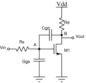
The common-source stage is one of the most common stages in an Op-Amp. The configuration is presented in figure2.20
Vdd
Vin Vout
M1 Rd
Figure 2.20: Common-source stage
One of the most important characteristic that this topology presents is the small-signal gain presented by:
Av= −gm(RD||ro) (2.40)
Analysing this configuration, this stage can be used to invert the signal due to the negative gain. It can be well used to increase the small-signal gain, if a correct combination of the transistor output resistance ro, and the load resistance RD. To have higher values of gain, the resistances
should be similar to have a high value of equivalent resistance. The voltage gain of this topology has a high dependence on the intrinsic parameters of the transistor, which can be prevented with a common-source stage with source degeneration, presented in figure2.21.
If a resistance is applied to the source of the input transistor and the expression of small-signal gain is:
Av=
−gmRD
1 + gmRs
(2.41) And the equivalent output impedance is:
Rout= RD||ro (2.42)
If gmRs>> 1, the gain expression is more dependent of the resistance ratio Av= −RRD s.
2.3 Operational Amplifiers with transparent TFT’s 23 Vdd Vin Vout M1 Rd Rs
Figure 2.21: Common-source stage with source degeneration
2.3.1.2 Source-Follower Stage
This stage is mostly used to connect high load impedance stages to low impedance stages, operat-ing as a voltage buffer. The schematic is presented in figure2.22.
Vdd
Vin
Vout M1
Rs
Figure 2.22: Source-follower stage
The small-signal gain for this stage is:
Av=
gm(Rs||ro)
1 + gm(Rs||ro)
(2.43) With the gm in this expression, the gain begins from zero with Vin= Vth, and increases with
higher values of Vin, with a approximation to 1. To have a lower dependence of the current to
the input voltage level, a transistor operating in saturation region can replace the resistor Rs. This
transistor will work as a current source. The output impedance is estimated by:
Rout= (1/gm)||Rs||ro (2.44)
Comparing with common-source stage, source-follower presents a lower output resistance, due to the low values of g1
24 Background
2.3.1.3 Common-Gate Stage
This stage presents the input voltage applied to the source of the transistor. The gate of the tran-sistor is biased with a DC voltage to operate in the saturation region. The schematic of this stage is presented in figure2.23. Vdd Vin Vout M1 Rd Vb
Figure 2.23: Common-gate stage
Analysing the small-signal gain, it can be estimated by:
Av= gm(RD||ro) (2.45)
This stage does not invert the signal and it has very low input impedance, due to the applied input at the source. The input impedance is estimated by:
Rin=
1 gm
(2.46) In multi-stage amplifiers, the low input impedance of this stage decreases the voltage gain of the previous stage. Besides, the saturation of the transistors is also necessary, so the biased transistor, due to its low impedance, has a low value of Vgs. Those are the disadvantages of this
configuration.
2.3.1.4 Cascode Stage
Comparing with common-source, cascode stage uses a biased transistor between the input tran-sistor and the output. This stage uses the same principles of common-gate stage with a current source, instead of a voltage, applied to the source of the biased transistor, using an input transistor. However, this stage has the disadvantage that the voltage level applied to the drain of the biased transistor must be enough to have the both transistors in saturation. This limits the value of RD,
and the small-signal gain. The schematic of this stage is presented in figure2.24. The small-signal gain can be estimated by:
Av= −
gm1 gm2
2.3 Operational Amplifiers with transparent TFT’s 25 Vdd Vin Vout M1 Rd Vb M2
Figure 2.24: Cascode stage
The expression of the gain is the same as the common-source small-signal gain. As the common-source stage, this configuration inverts the signal applied. The advantages of this con-figuration is the very high output impedance, due to the large number of transistors. The output resistance is estimated by:
Rout= [1 + gm2ro2]ro1+ ro2 (2.48)
The main effect that this stage has is the elimination of Miller effect on the input transistor, increasing the bandwidth response.
2.3.2 Differential Pair
This configuration is one of the most important because it receives the two differential inputs of the amplifier. The schematic of this configuration is presented in figure2.25.
Vdd M1 Rd Rd Vin2 Vin1 Vb M2 M3 Vout2 Vout1
Figure 2.25: Differential pair
To analyse the differential pair theoretically, it can be assumed that the relation Vin1− Vin2
26 Background
so the transistor M1 is off, so Vout1= VDD and M2is on, so Vout2= VDD− RDISS. If the difference
between Vin1− Vin2 becomes smaller, the output voltage tends to be Vout1= Vout2= VDD−RD2ISS.
If Vin1− Vin2 becomes positive, the output voltages change in a symmetrical way. This is how
the amplifier regulates the output voltage depending of the values at the input. The differential gain of this configuration take into account the two inputs, which have two components each, the differential and the common-mode. They are defined as:
Vin1=Vin1−Vin2
2 +
Vin1+Vin2
2 (2.49)
Vin2=Vin2−Vin1
2 +
Vin1+Vin2
2 (2.50)
To calculate the differential gain, there is only the differential component that is defined as input, as if there was applied a virtual ground between the sources of M1 and M2, so the output
voltages are: Vout1= −gm(RD||ro1) Vin1−Vin2 2 (2.51) Vout2= −gm(RD||ro2) Vin1−Vin2 2 (2.52)
Considering that there is no common-mode component, the differential gain is expected to be:
Ad= Vout1−Vout2= −gm(RD||ro)(Vin1−Vin2) (2.53)
The differential pair should eliminate the effect of common-mode perturbations, but in reality the circuit is not fully symmetric due to the fabrication and the output impedance of M3 is not
infinite. Because of these facts, the common-mode variation exists, and its gain, considering a fully symmetric circuit and a finite output impedance of M3, is estimated as:
Av,CM= Vout Vin,CM = − RD/2 (1/2gm) + ro3 (2.54) This component of gain can disturb the bias point and limit the output voltage swing. Besides, the non-symmetrical circuits create a difference on the currents between each side, increasing the issues mentioned. For all these reasons, the common-mode effect should be suppressed as much as possible, to have a very high common-mode rejection ration determined by:
CMRR= 20log10(
Ad
|ACM|
) (2.55)
2.3 Operational Amplifiers with transparent TFT’s 27
2.3.3 Multi-Stage Amplifiers
In order to have high gain amplifiers with low output impedance, single-stage amplifiers are not enough, so there should be used multiple stages. However, with more stages used, there are applied more poles, and zeros in some cases, due to the resistances and capacitances added. This fact can produce an unstable behaviour of the amplifier under feedback, if there are dominant poles applied at high frequencies, decreasing the phase margin. To understand the principles of stability and frequency response of the amplifier, it is necessary to know in which way the poles and zeros are introduced in the phase, their origins and how to compensate their drawbacks.
2.3.3.1 Miller Effect
Miller’s theorem describes one of the most important effects in analog circuits. It is related with the amplifier and the introduction of poles and phase response. This theorem states that a circuit presented in figure2.26a can be converted in the circuit of figure2.26bif Z1= Z/(1 − Av) and
Z2= Z/(1 − A−v1), where Av= Vy/Vx. Z X Y (a) (a) Z1 X Y Z2 (b) (b)
Figure 2.26: Application of Miller effect to a floating impedance
The importance of this theorem in amplifiers can be presented with the circuit in figure2.27, that represents a common-source stage with the equivalent parasitic capacitances of a TFT, CGS
and CGD. The equivalent capacitances connected to the ground, with a equivalent impedance of
the capacitor of ZC= 1/(sC), for the node A is CA= CGS+ (1 − Av)CGD and for the node B is
CB= (1 − A−v1)CGD. Due to the gain of the common-source stage Av= −gmRDis larger that unity,
analysing the two nodes capacitances, it is considered that the capacitance at the input of the stage is higher than in the output, due to the Miller multiplication factor of CGD. Therefore, the pole
associated to the input is at lower frequencies.
2.3.3.2 Stability and Frequency Compensation
The capacitances and resistances associated to the amplifier have an important role on the stability and frequency response of the circuit. In fact, as non-dominant poles at higher frequencies worsens the phase responses, due to the lower phase margin introduced by a phase shift at high frequencies. That influences critically the stability of the amplifier under feedback. Frequency Compensation is the method to have better frequency responses. The frequency compensation can be made with additional capacitors or resistors in the circuit nodes where there are dominant poles, in order to
28 Background
Figure 2.27: Common-source stage with parasitic capacitances
pull it into lower frequencies, resulting in higher phase margin. This technique is better explained in the chapter4, where the frequency compensation of the proposed regulator is described.
Chapter 3
Bibliographic Review
There is not that many reports on transparent DC/DC Converters, but the ones that exist, invari-ably use voltage multipliers topologies instead of inductors. Besides, they use different switching modes. In transparent electronics, switches or diodes may be created with transistors. Therefore, the study of TFT is also very important to refer. This chapter starts with a review of research made for transparent TFTs with a-IGZO, with a historical perspective. Then, it is presented an overview of DC/DC converter proposals made until now. The initial topologies presented in charge-pumps section are not designed with transparent electronics, but they represent a step-forward to an effi-cient design of a switched-capacitor DC/DC converter. The next section presents the topologies that have been designed to regulate DC/DC converters. Last sections present an overview of the improved characteristics and a conclusion for the proposal presented in this report.
3.1
Thin-Film Transistors using a-IGZO
The production of transparent thin-film transistors have improved during the years with well-performed researches. This section does not intend to present an exhaustive report on all success-ful studies made with transparent TFT. However, a historical perspective on the basic behaviour improvements of these devices, with examples of some articles from different years, will be dis-cussed.
The first TFT using a-IGZO in channel layer was reported by K. Nomura et al. [16] in 2004. It is a n-type TFT, where a-IGZO was deposited at room temperature by pulsed laser deposition on polyethylene terephthalate substract, creating a staggered top-gate structure. Insulator is 140 nm thick and the channel with a length of 50µm and a width of 200µm. The estimation for saturation mobility is 8.3cm2/V.s with a drain-source current of 0.02mA, VGS= 5V and a leakage current of
10−10A. Field effect mobility is 5.6cm2/V.s.
P. Barquinha et al. [20] in 2008 reported an a-IGZO TFT with saturation mobility of 18.7cm2/V.s, 29
30 Bibliographic Review
field-effect mobility of 24.5cm2/V.s, maximum drain-source current of 0.08mA and threshold volt-age Vth= 12.8V . The transistor was created in a staggered bottom-gate structure with a 100 nm
thick SiO2 gate dieletric, a Ti/Au contacts with 15 nm and 135 nm of thickness, respectively,
and 50 nm-thick a-IGZO layer deposited by RF sputtering. Annealing was performed after all depositions.
In 2009, K. Nomura et al. [29] reported a bottom-gate TFT with saturation mobility of 12.6cm2/V.s and a threshold voltage between 1.4 V and 1.8 V. TFT’s were created on SiO2
sub-strate. A 40 nm-thick a-IGZO was deposited by pulsed laser deposition with oxygen partial pres-sure and a width and length of 300 and 50 µm, respectively. The device was subjected to annealing with water vapour at partial pressure, and Ti/Au were used for source/drain contacts.
A. Suresh et al. [30] in 2010 created an a-IGZO TFT using staggered bottom-gate structure. Gate dielectric was deposited with 120 nm-thick Al2O3with atomic layer deposition. A 40
nm-thick a-IGZO layer and 200 nm-nm-thick indium tin oxide were created by physical vapour deposition. No annealing steps were employed. The authors present a threshold voltage of 3.5 V and saturation field effect mobility of 15cm2/V.s with VDS= 20V . There was reported a leakage current of 1pA.
S. Hong et al. [10] use in their transparent DC/DC converters a-IGZO TFT with co-planar top-gate structure. As source-drain material, there is deposited by sputtering indium-tin oxide. For the insulator there was used Al2O3deposited by atomic layer deposition at 150oCThe results
present a threshold voltage of -0.8V to reach a drain current of 100pA, 20.6cm2/(V.s) of field effect mobility and a subthreshold slope of 0.2 V/dec at room temperature.
D. Kang et al. [31] created in 2011 a TFT using co-planar top-gate structure. On 200 nm-thick glass substrate, a 20 nm-nm-thick a-IGZO layer was deposited using sputtering. For insulator, the authors used 200 nm-thick SiO2 and patterned molybdenum for gate electrodes. After
pat-terning a-IGZO and etched SiO2, a 400 nm-thick SiNxlayer was deposited. Then, a 200 nm-thick
molybdenum was deposited for source-drain contacts. With VG= 20V , field-effect mobility is
24.7cm2/V.s in saturation mode and 21cm2/V.s in linear mode. Threshold voltage is around 3.6 V.
The different studies made suggests a improvement on TFT behaviour, with better field-effect mobility, lower threshold voltage and lower resistance. During the years, various materials for insulators and source-drain contacts were tested and results were compared. For channel layer, a-IGZO is actually the material with best performance. For the source-drain contacts, the main materials reported with better results are Ti/Au and molybdenum. Analysing the performance of the TFT depending of the structure used, the recent reports suggest better results of mobility with a top-gate structure, due to the better isolation of the channel to external factors. The transparent TFT fabricated in CENIMAT use the staggered bottom-gate structure, so the performance of the transistor in terms of mobility is not expected to be higher than 20cm2/(V.s). The effects of
3.2 Charge-Pumps 31
high on-resistance in charge-pumps and DC/DC converters using switched-capacitor stages were discussed in chapter2.
3.2
Charge-Pumps
This section presents the charge-pumps designed during the years. Initially, there is considered the first topologies in non-transparent electronics. Later, the configurations designed with transparent TFT’s.
3.2.1 Non-transparent designs
3.2.1.1 Initial Configurations
The first charge-pump reported are dated from 1932, with the Cockcroft-Walton multiplier [3]. As mentioned in the last chapter, it used clock signals to charge the capacitors and diodes through the main path, increasing the voltage in the output to an expected voltage of 2VDD. However, the
circuit has some constrains. One of them is that the coupling capacitors C must have a much larger value of capacitance than the stray capacitances Cs, to have an efficient voltage increase.
Due to the high values of stray capacitance in the substrate of monolithic circuits, the circuit has limitations on efficient voltage multiplication. Besides, the voltage drop associated to the diodes limits the output voltage level even with a large number of stages. With transparent technology, diodes are replaced by TFT’s, which several constrains were discussed such as the on-resistance and voltage drop.
Another initial configuration referred in the last chapter is the Dickson’s charge-pump dated from 1976 [4]. This is a improve of the Cockcroft-Walton configuration, due to the connected pump capacitors directly to the ground. According to the author, this enables a smaller difference between the coupling and stray capacitances, in order to have efficient multiplication of voltage. Although the problem with stray capacitances is reduced, the voltage drop across the diodes is not avoided. Furthermore, there is a high threshold voltage needed for the transistors, due to the differentiation between switching stages, and a large voltage drop across the transistor when the following capacitor is transferring its charge. These facts increase the parasitic capacitances associated to the circuit, according to Baderna [28]. These capacitances reduce the time response of the circuit and the maximum frequency allowed, resulting in worse response of the circuit to the load currents.
3.2.1.2 Cross-connected Configuration
P. Favrat et al. [7] proposed a new voltage doubler with cross-connected transistors to reduce the parasitic capacitances, improving the charge-pump cell from Y. Nakagome et al. [32] with a double series switch of p-type transistors. The circuit is presented in figure3.1.
With the two series p-type transistors added, the author refer that the load capacitor have not to be very high, without affecting the charge-pump efficiency. The cross-connection reduces
32 Bibliographic Review Vdd Vout CLK1 CLK2 C C M1 M2 M3 M4 M5 M6 Cb Cout
Figure 3.1: Cross-connected configuration from P. Favrat et al. [7]
the voltage drop on the transistors to a value lower than VDD, because when one capacitor is
discharging, the opposite side is charging, creating a full reverse bias of the junctions. The on-resistance is also lower, due to the synchronization of boosting on gate transistors.
The Favrat voltage doubler, with a cross-connected topology, has transistors with lower par-asitic capacitance than the first topology, increasing the efficiency. Theoretically, Baderna [28] estimates the Dickson’s charge-pump efficiency as 44.8%, and 56% for the Favrat’s doubler ef-ficiency. The p-type transistors can be substituted by a diode-connected TFT’s, to answer to the transparent constrains.
3.2.1.3 Switch Bootstrapping Technique
The parasitic capacitance and output voltage level are two of the main concerns when a DC/DC converter using charge pumps topology is created. According to Y. Allasasmeh and S. Gregori [8], the usage of bootstrapping switches prevents short-circuit losses, due to the precision in controlling the switching times, and enables good efficiency with low supply voltage, due to a lower switch on resistance and lower power losses. The schematic of bootstrapping topology for a voltage doubler is presented in figure3.2. Vdd Vdd Vout Nb1 Nb2 N1 N2 Cn1 Cn2 P1 P2 Pb1 Pb2 Cp1 Cp2 C1 C2 CLK1 CLK2 CLK2 CLK1 CLK1 CLK2 CLK1 CLK2 Nd2 Nd1 Pd1 Pd2
3.2 Charge-Pumps 33
Due to the added transistors and capacitances are not in the main current path between VDD
and Vout, the authors [8] refer that their area can be reduced, decreasing the parasitic capacitances.
This phenomenon is helped with the fact that the gates of the first transistors are not connected to the main current path. They also report a higher output voltage in 1.5% due to this fact.
3.2.1.4 Switched-Capacitor based Embedded DC-DC Buck Converter
B. Maity and P. Mandal [9] present a non-transparent device that uses switched-capacitors to create a step-down DC/DC converter. The importance of this reference is the use of concepts that can be applied on the desired transparent DC/DC converter. The design is presented in figure3.3.
Vdd M1 M5 M2 M6 M3 M7 CL RL Vout Cf1 Cf2 M8 M4 1 2 2 1
Figure 3.3: Switched Capacitor based Buck Converter [9]
Internal signals are used to control half of the switches, in order to reduce switching power loss and output ripple noise. The circuit shown in figure3.3is repeated 11 times and their output connects together with load capacitor and current source.
For a 10 mA current, results present a 1.35 V, with an input voltage range between 2.9 V and 3.8 V. For this voltage level, and a 25 mA load current, output ripple is 8 mV. Efficiency established on 79.5% for a load current between 1 mA and 25.5 mA. When the output voltage increases to 1.55 V, with load current from 1 mA to 7 mA, a peak power efficiency of 87% is achieved. This proposal uses p-type transistors, which can easily be replaced by n-type.
3.2.2 Configurations with TFT’s
3.2.2.1 DC/DC Converters using Indium Gallium Zinc Oxide Thin-Film Transistors S. Hong et al. [10] present the most close device to what we need to achieved. The proposed positive DC/DC Converter is presented in figure3.4.
It has eight n-type IGZO TFT’s, four pumping capacitors and two storage capacitors. When CLK= 1, the voltage level of node D is 2VDDbecause it receives the energy stored on capacitor C1.
![Figure 2.4: Transparent capacitor from cross-sectional view [1]](https://thumb-eu.123doks.com/thumbv2/123dok_br/15582809.1049482/24.892.280.571.922.1075/figure-transparent-capacitor-from-cross-sectional-view.webp)
![Figure 2.18: Charge-Pump Step-Up Converter [6]](https://thumb-eu.123doks.com/thumbv2/123dok_br/15582809.1049482/37.892.309.624.693.863/figure-charge-pump-step-up-converter.webp)
![Figure 2.19: Charge-Pump Step-Down Converter [6]](https://thumb-eu.123doks.com/thumbv2/123dok_br/15582809.1049482/38.892.262.584.915.1078/figure-charge-pump-step-down-converter.webp)
![Figure 3.2: Bootstrapping configuration of charge-pump from Allasasmeh and Gregori [8]](https://thumb-eu.123doks.com/thumbv2/123dok_br/15582809.1049482/50.892.263.582.831.1079/figure-bootstrapping-configuration-charge-pump-allasasmeh-gregori.webp)
![Figure 3.3: Switched Capacitor based Buck Converter [9]](https://thumb-eu.123doks.com/thumbv2/123dok_br/15582809.1049482/51.892.342.590.396.643/figure-switched-capacitor-based-buck-converter.webp)
![Figure 3.4: Transparent Step-Up DC/DC Converter [10]](https://thumb-eu.123doks.com/thumbv2/123dok_br/15582809.1049482/52.892.297.554.138.451/figure-transparent-step-up-dc-dc-converter.webp)
![Figure 3.6: Cross-coupled DC/DC converter [10]](https://thumb-eu.123doks.com/thumbv2/123dok_br/15582809.1049482/53.892.341.594.136.357/figure-cross-coupled-dc-dc-converter.webp)
![Figure 3.9: Proposal of linear regulator from Bhattacharyya et al.. Image obtained in [12]](https://thumb-eu.123doks.com/thumbv2/123dok_br/15582809.1049482/55.892.290.638.520.765/figure-proposal-linear-regulator-bhattacharyya-et-image-obtained.webp)
