MODELING AND CONTROL OF A THREE-PHASE ISOLATED
GRID-CONNECTED CONVERTER FOR PHOTOVOLTAIC
APPLICATIONS
Marcelo Gradella Villalva
∗Thais Gama de Siqueira
†Marcos Fernando Espindola
∗Ernesto Ruppert
∗ [email protected]∗UNICAMP - UNIVERSITY OF CAMPINAS, BRAZIL
†UNIFAL - UNIVERSITY OF ALFENAS AT PO ¸COS DE CALDAS, BRAZIL
ABSTRACT
This paper describes the modeling and control of a three-phase grid-connected converter fed by a photo-voltaic array. The converter is composed of an iso-lated DC-DC converter and a three-phase DC-AC volt-age source inverter The converters are modeled in order to obtain small-signal transfer functions that are used in the design of three closed-loop controllers: for the out-put voltage of the PV array, the DC link voltage and the output currents. Simulated and experimental results are presented.
KEYWORDS: grid-connected, photovoltaic, converter, PV
RESUMO
Modelagem e controle de um conversor trif´asico
conectado `a rede para aplica¸c˜oes fotovolt´aica Este artigo descreve a modelagem e o controle de um conversor trif´asico conectado `a rede alimentado por um conjunto fotovoltaico. O conversor ´e composto de um est´agio CC-CC isolado um est´agio CC-CA. S˜ao obtidas
Artigo submetido em 04/12/2009 (Id.: 01090) Revisado em 13/04/2010, 31/08/2010
Aceito sob recomenda¸c˜ao do Editor Associado Prof. Darizon Alves de An-drade
fun¸c˜oes de transferˆencia com as quais s˜ao projetados trˆes sistemas de controle em malha fechada: um para a tens˜ao de entrada do arranjo de pain´eis solares, um para a tens˜ao do do barramento de tens˜ao cont´ınua e outro para as correntes trif´asicas de sa´ıda.
PALAVRAS-CHAVE: conversor, fotovoltaico, conectado `a rede
1
INTRODUCTION
The aim of this paper is to describe the modeling and control design of a three-phase grid-connected converter for photovoltaic (PV) applications. The converter has two stages: an isolated DC-DC full-bridge (FB) and a three-phase DC-AC inverter with output current con-trol. The converters are modeled in order to obtain small-signal transfer functions that are used in the de-sign of linear closed-loop controllers based on propor-tional and integral (PI) compensators.
Fig. 1 shows the blocks that constitute the system stud-ied in this paper. The PV array feeds the DC-DC full-bridge FB converter, which in turn feeds the three-phase DC-AC inverter. Three controllers are used in the sys-tem. The control block of the DC-DC converter contains the controller of the input voltagevpv of the converter,
DC-+
-+
-PV array
DC-DC DC-AC
converter converter
A
C
g
ri
d
control control
vpv vlink
ia,b,c
Figure 1: Block diagram of the PV system.
0 5 10 15 20 25 30
0 1 2 3 4 5 6 7 8 9
V [V]
I [A]
KC200GT linear model MPP
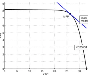
Figure 2: Nonlinear I-V characteristic of the solar array and curve of the equivalent linear model at the MPP.
AC control block contains the controller of the DC link capacitor (the capacitor that connects the DC-DC and DC-AC converters) voltagevlinkand another for the
si-nusoidal three-phase output currentsia,b,c. This kind of
two-stage PV system has also been reported in (de Souza et al., 2007) using an analog control approach.
2
MODELING THE PV ARRAY
The PV array presents the nonlinear characteristic il-lustrated in Fig. 2. In this example the KC200GT (Kyocera, n.d.) solar array is used. The dynamic behav-ior of the converter depends on the point of operation of the PV array. Because the array directly feeds the con-verter it must be considered in the dynamic model of the converter. A PV array linear model will be necessary for modeling the DC-DC converter in next section. The system is modeled considering that the PV array oper-ates at the maximum power point (MPP) with nominal conditions of temperature and solar irradiation.
The equation of the I-V characteristic is given by (Villalva et al., 2009a), (Villalva et al., 2009b):
I=Ipv−I0
exp
V +R
sI
Vta
−1
−V +RsI
Rp
(1)
where Ipv and I0 are the photovoltaic and saturation
currents of the array, Vt = NskT /q is the thermal
voltage of the array with Ns cells connected in
se-ries, Rs is the equivalent series resistance of the
ar-ray, Rp is the equivalent shunt resistance, and a is
the ideality constant of the diode. The parameters of the PV array equation (1) may be obtained from measured or practical information obtained from the datasheet: open-circuit voltage, short-circuit current, maximum-power voltage, maximum-power current, and current/temperature and voltage/temperature coeffi-cients. A complete explanation of the method used to determine the parameters of the I-V equation may be found in Villalva et al. (2009a) and Villalva et al. (2009b).
As the PV system is expected to work near the max-imum power point (MPP), the I-V curve may be lin-earized at this point. The derivative of theI-V curve at the MPP is given by:
g(Vmp,Imp) =−
I0
VtNsa
exp
V
mp+ ImpRs
VtNs
− 1
Rp
(2)
The PV array may be modeled with the following linear equation at the MPP:
I= (−gVmp+Imp) +gV (3)
Fig. 2 shows the nonlinearI-V characteristic of the Ky-ocera KC200GT solar array superimposed with the lin-ear I-V curve described by (3). The parameters of the I-V equation obtained with the modeling method pro-posed in Villalva et al. (2009a) and Villalva et al. (2009b) are listed in Table 1. From these parameters, with (2) and (3), the equivalent voltage source and series resis-tance of the solar array linearized at the MPP are ob-tained: Veq= 51.6480 V andReq= 3.3309 Ω.
3
DC-DC FULL-BRIDGE CONVERTER
3.1
Modeling
ob-Table 1: Parameters of the KC200GT solar photovoltaic array at nominal operating conditions.
Imp 7.61 A
Vmp 26.3 V
Pmax 200.143 W
Voc 32.9 V
I0,n 9.825·10−8A Ipv 8.214 A
a 1.3
Rp 415.405 Ω
Rs 0.221 Ω
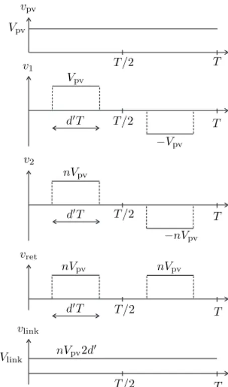
serving the approximate voltage waveforms of Fig. 4. By replacing the instantaneous voltages and currents by their average values it is possible to obtain an average equivalent circuit without the switching elements (tran-sistors and diodes) and the transformer contained in the dashed box with terminals1-2-3-4. This modeling method is described in Erickson e Maksimovic (2001), Middlebrook (1988), Middlebrook e Cuk (1976) and was used in Villalva e Ruppert F. (2008b), Villalva e Rup-pert F. (2008a), and Villalva e RupRup-pert F. (2007) in the modeling of the input-controlled buck converter, which is very similar fo the modeling of the FB converter used in this paper.
iL iin,inv
ipv iin,fb
vlink
vret
L
Cpv Clink
vpv v1 v2
+ +
+ +
+
−
− − −
−
1 2
3 4
Figure 3: Isolated full-bridge DC-DC converter.
By observing the circuit terminals1-2-3-4the following equations may be written, where average values within one swithing periodT are marked with a bar over the variable:
¯
vret=dv¯pvn (4)
¯iin,fb=d¯iLn (5)
where ¯vret is the average output voltage of the rectifier,
¯
vpv is the average voltage at the input of the converter,
T T T T T
T /2
T /2
T /2
T /2
T /2
vpv
v1
v2
vret
d′T
d′T
d′T
Vpv
Vpv
−Vpv
nVpv
nVpv
nVpv
−nVpv
Vlink
vlink
nVpv2d′
Figure 4: Approximate voltage waveforms of the FB converter.
_
+
+ +
+
− −
− DC
DC
< iL> < iin,inv>
< ipv> < iin,fb>
< vlink>
< vret>
L Cpv < vpv> Clink
1 2
3 4
1 : 2d′n
Veq
Req
Figure 5: Equivalent average circuit of the FB converter.
¯iin,fb is the average input current, ¯iL is the average in-ductor current,nis the primary to secondary turns ratio of the transformer, and dis the effective duty cycle of the converter defined asd= 2d′.
With (4) and (5) the equivalent circuit of Fig. 5 is ob-tained, where Veq and Req are the equivalent voltage
and resistance of the linear PV array model obtained in previous section.
The average state equations of the circuit of Fig. 5 are:
Veq−v¯pv
Req =Cpv
d¯vpv
dt + ¯iin,fb (6)
¯
vret−v¯link=Ld¯iL
The state equations (8) and (9) are obtained by replac-ing (4) and (5) in (6) and (7):
Veq−v¯pv
Req =Cpv
d¯vpv
dt + ¯iLdn (8)
dn¯vpv−¯vlink=L
d¯iL
dt (9)
The average variables may be separated in steady-state and small-signal components (Erickson e Maksimovic, 2001):
¯
vpv= Vpv+ ˆvpv (10)
¯
vlink= Vlink+ ˆvlink
¯iL= IL+ ˆiL d= D−dˆ
With the definitions of (10), with ˆvlink = 0, from (8)
and (9) the state equations (11) and (12) are obtained:
Veq
Req−
(Vpv+ ˆvpv)
Req =Cpv
dˆvpv
dt +n(DIL+DiˆL−dIˆL−dˆiˆL) (11)
n(DVpv+Dvˆpv−dVˆ pv−dˆvˆpv) =L
dˆiL
dt (12)
From (11) and (12), by neglecting the nonlinear terms ndˆˆiLandndˆvˆpvand by applying the Laplace transform,
the small-signals-domain state equations are obtained:
−vˆpv(s)
Req
=sCpvvˆpv(s) +nDˆiL(s)−dˆ(s)ILn (13)
nDvˆpv(s)−dˆ(s)Vpvn=LsˆiL(s) (14)
from which the small-signal transfer functionGvd(s) of
the converter input voltage is obtained:
Gvd(s) = ˆvpv(s)
ˆ d′(s) =
Req(sLILn+n2DVpv)
s2R
eqLCpv+sL+n2D2Req (15)
TheGvd(s) transfer function describes the behavior of
the full-bridge converter input voltage with respect to
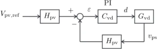
ε Vpv,ref Hpv
Hpv
Gvd
Cvd
d
vpv PI
+
−
Figure 6: Controller of the input voltage vpv of the FB
con-verter.
Table 2: Parameters of the2×15PV array with the KC200GT
solar array module.
Ipv,mp 15.22 A
Vpv,mp 394.50 V
Req 24.9816 Ω
Veq 774.7194 V
the control variable ˆd′ = 1−dˆ. Due to the presence
of the turns ratio n in the model the error of the lin-ear model represented by the transfer function increases proportionally to n. This problem is not observed in conventional converter models whose output voltage is controlled. So it is important, mainly ifnis not a small number, to model the converter as near as possible the operating point of the PV array – this is possible with the linear model developed in previous section.
3.2
Control
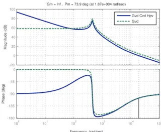
Fig. 6 shows the input voltage controller of the FB con-verter based on a PI compensator. The PI may be designed with conventional feedback control techniques to meet any desired specifications of bandwidth, phase margin, etc.
As an example, a FB converter control system is de-signed to operate with a 6 kW (peak) PV array com-posed of 2×15 KC200GT modules. In section 2 the parameters and the equivalent linear model at the MPP of the KC200GT module where obtained. The parame-ters of the linear model of the 2×15 array are presented in Table 2. Table 3 presents the system parameters from which theGvd(s) transfer function is obtained:
Gvd(s) = 20000.0 + 3.7s
0.00012s2+ 0.0050s+ 25.0 (16)
The converter is designed considering a switching fre-quency fsw = 20 kHz. A good practice is to choose
steady-state control error, with a satisfactory phase margin and bandwidth of approximately 3 kHz, with feedback gain Hpv= 0.002,Cvd(s) is designed as:
Cvd(s) =
300 (s+ 100)
s (17)
Fig. 7 shows the Bode plot of the compensated loop Gvd(s)Cvd(s)Hpv.
4
THREE-PHASE
GRID-CONNECTED
DC-AC INVERTER
Fig. 8 shows the three-phase inverter connected to the AC grid through the coupling inductorsLac. The
verter receives DC voltage and current from the FB con-verter and delivers active power to the grid with sinu-soidal currents. The output currents ia,b,c are
synthe-sized by current controller of section 4.1 and the DC link capacitor voltage vlink is kept at the steady valueVlink
by the voltage controller studied in section 4.2.
Table 3: Parameters used in the modeling of the FB converter and in the design of the voltage controller.
Ipv 14.99 A
Vpv 400 V
Veq 774.7194 V
Req 24.98 Ω
C 1000µF
L 5 mH
Vlink 400 V
D 0.5
fsw 20 kHz
n 2
4.1
Synthesis of the sinusoidal output
cur-rents
1) Modeling - The process of modeling the three-phase grid-connected converter with controlled output cur-rents (Buso e Mattavelli, 2006) is based on the equiva-lent circuit of Fig. 9. Considering the converter is driven by a sinusoidal PWM modulator with symmetrical tri-angular carrier, it can be modeled as a constant gain, being m the PWM modulation index. Each phase of the converter is analyzed independently with the equiv-alent circuit of Fig. 9 and the inductor current transfer function is:
Gim(s) =
ˆia,b,c ˆ
m =
Ginv
s Lac
= Vlink 2s Lac
(18)
-20 0 20 40 60 80 100
Magnitude (dB)
100 101 102 103 104 105 -180
-135 -90 -45 0
Phase (deg)
Gm = Inf , Pm = 73.9 deg (at 1.87e+004 rad/sec)
Frequency (rad/sec)
Gvd Cvd Hpv Gvd
Figure 7: Bode plots of the full-bridge DC-DC converter transfer function Gvd(s) and of the compensated loop
Gvd(s)Cvd(s)Hpv.
+
-Lac
Lac
Lac
ia
ib
ic
vsa
vsb
vsc
iL iin,inv
vlink Cpv
va
vb
vc
n grid
Figure 8: Three-phase grid-connected DC-AC converter.
2)Control with PI compensators - The output currents of the grid-connected converter can be synthesized by the current controller of Fig. 10, which is composed of three PI compensators that determine the modulation indexes of each of the sinusoidal PWM modulators that drive the three phases of the converter. The references of the output currents,i{a,b,c},ref, are sinusoidal waveforms
originated from the DC link voltage controller explained in next section.
The PI compensators with transfer functionCim(s) are
designed using the same principles used in section 3.2. For example, with the parameters of Table 4 the system transfer function and the PI compensator are:
Gim(s) = 200
0.005s+ 1, Cim(s) =
7.9 (s+ 1000)
s (19)
Lac
ia
vsa
m Ginv va
Figure 9: Single-phase equivalent circuit of the grid-connected converter output.
ia
ib
ic
ma
mb
mc
Gim
εa
εb
εc
phase a
phase b
phase c
ia,ref
ib,ref
ic,ref
Hiac
Hiac
Hiac
Hiac
Hiac
Hiac
PWM PWM PWM
inverter inverter inverter
PI PI PI
Cim
Cim
Cim
+ + +
− − −
Figure 10: Controller of the output currents of the DC-AC con-verter in stationary coordinates.
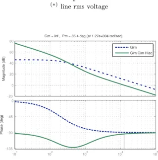
phase margin and low steady state error. Fig. 11 shows the bode plots ofGim(s) and of the compensated loop
Gim(s)Cim(s)Hiac.
3)Control with PI compensators in the synchronous ref-erence frame - The quality of the three-phase currents synthesis may be significantly improved with the syn-chronous current controller illustrated in Fig. 12. The transformation of the abc currents to the synchronous dq frame permits to cancel the current steady state er-ror (Buso e Mattavelli, 2006) because the currents in the fundamental frequency become DC quantities. This transformation also gives the controller excellent imu-nity to integrator saturation caused by offsets in the measured currents. The current controller of Fig. 12 employs two PI compensators for the dandqcurrents. Thedq-abcandabc-dq transformations are presented in the appendix 1. The transformations employ the angle θ (syncronized with the grid voltages) provided by the phase-locked loop (PLL) of Appendix 2.
Table 4: Parameters of the grid-connected converter system.
Hiac 1/25
Hvlk 1/500
Clink 4700µF
Lac 2 mH
Vlink 400 V
fsw 10 kHz
Vac(∗) 220 V
(∗) line rms voltage
-20 0 20 40 60 80
Magnitude (dB)
101 102 103 104 105 -135
-90 -45 0
Phase (deg)
Gm = Inf , Pm = 86.4 deg (at 1.27e+004 rad/sec)
Frequency (rad/sec)
Gim Gim Cim Hiac
Figure 11: Bode plots ofGim(s) andGimCim(s)Hiac.
ia
ib
ic
ma
mb
mc
εa
εb
εc
ia,ref
ib,ref
ic,ref
Hiac
Hiac
Hiac
Hiac
Hiac
Hiac
PI PI
Cim
Cim
abc→dq dq→abc
eq. (28) eq. (29)
eq. (30) eq. (31)
md
mq ed
eq
θ1 θ1
PLL +
+ +
− − −
grid voltages
Clink
< vlink>
< iL> < iin,inv> +
−
Figure 13: Equivalent circuit of the DC link charge.
According to the theoretical analysis presented in (Buso e Mattavelli, 2006), the PI compensators of the syn-chronous frame controller may be designed exactly like the single-phase compensators used in the conventional stationary frame current controller presented in previous section, except that the integral gain of the synchronous frame PI is twice the gain of the conventional single-phase PI. The implementation of the PI compensators used in both stationary and synchronous controllers is explained in Appendix 3.
4.2
Control of the DC link voltage
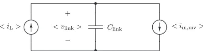
1)Modeling - The circuit of Fig. 13 shows the DC link capacitor and two equivalent current sources replacing the DC-DC and DC-AC converters. The capacitor re-ceives energy from the DC-DC converter and delivers it to the DC-AC inverter. The difference between the input and output charges increases or decreases the ca-pacitor voltage. The average input and output currents (and consequently the converter input and output pow-ers) must be in equilibrium so that the average capacitor voltage is constant.
The following power balance equations may be written:
< vlink>< iin,inv>= 3Vac(rms)Iac(rms) (20)
< iin,inv>=
3Vac(rms)Iac(pk)
< vlink> √
2 (21)
where Vac(rms) and Iac(rms) are the per-phase rms grid
voltage and current.
Eq. (22) may be simplified considering the average pacitor voltage is approximately constant. Both the ca-pacitor and voltage control time constants are large, so:
< iin,inv>=
3Vac(rms)Iac(pk)
Vlink√2
(22)
From the circuit of Fig. 13 the following average state equation is obtained, considering< iL>=IL:
IL−Clinkd< vlink>
dt −< iin,inv>= 0 (23)
Because one are interested in finding a small-signal equa-tion of the capacitor voltage and of the converter in-put current, the assumptions < vlink >= Vlink and
< iL >= IL where conveniently used in the average
power equation (22) and in the state equation (23), re-spectively. From (22) and (23):
IL−Clinkd< vlink>
dt =
3Vac(rms)Iac(pk)
Vlink √
2 (24)
Replacing< vlink>=Vlink+ ˆvlinkandIac(pk)= ¯Iac(pk)+
ˆ
Iac(pk) in (24) and applying the Laplace transform
re-sults the following small-signals-domain state equation:
s Clinkˆvlink(s) =
3Vac(rms)Iˆac(pk)(s)
Vlink √
2 (25)
From (25) the DC link voltage transfer funcion is ob-tained:
Gvlk(s) =
ˆ vlink(s)
ˆ
Iac(pk)(s)
= 3Vac(rms)
s ClinkVlink √
2 (26)
The transfer function of (26) is consistent with the transfer function developed in (Barbosa et al., 1998), where the authors used a different approach and ob-tained a similar equation.
2)Control - The controller of Fig. 14 is used to regulate the DC link voltage. The PI compensator with trans-fer function Cvlk(s) determines the peak of the output
sinusoidal currents. Three unit sinusoidal signals syn-chronized with the grid voltages are multiplied by the PI output Iac(pk). These multiplications generate the
current references used by the current controller of sec-tion 4.1, Fig. 10. The balance of the input and output powers of the DC link capacitor is achieved by regulat-ing the amplitudes of the sinusoidal currents injected in the grid.
Fig. 15 shows the equivalent control loop of the DC link voltage with theGvlk(s) transfer function (26) obtained
in last section.
With the scheme of Fig. 15 it is possible to design the compensatorCvlk(s) in order to achieve the control of
Cvlk
Hvlk
Hvlk
vlink
Vlink,ref ε
ia,ref
ib,ref
ic,ref
Iac(pk)
vsan
vsbn
vscn
PI
3-φPLL +
−
× × ×
Figure 14: DC link voltage controller.
Ipk
Cvlk Gvlk
Hvlk
Hvlk
vlink
Vlink,ref
ε
+
−
Figure 15: Equivalent control loop of the DC link voltage.
the following transfer function and compensator (27) are obtained:
Gvlk(s) =202.2
s , Cvlk(s) =
1553 (s+ 10)
s (27)
The bandwidth of the control loop is made intention-ally low so that the DC link voltage control will not cause disturbances in the sinusoidal output currents of the converter. The amplitudes of the currents are reg-ulated so that the average DC link capacitor voltage is constant. The amplitudes of the currents are practically constant when the system is in steady state.
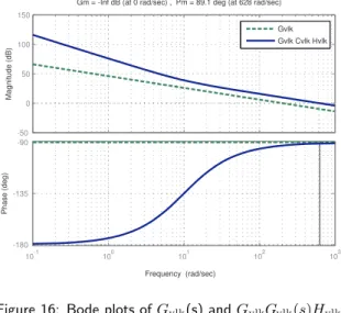
Fig. 16 shows the Bode plots of the equivalent transfer function of the DC link capacitor voltage and of the compensated system. The bandwidth of the control loop is adjusted near 100 Hz with the PI compensator of (27) and the zero located ats=−10 rad/s warranties a low steady state error.
5
SIMULATION RESULTS
This section presents results of simulations of the DC-DC and DC-DC-AC converters. The aim of these simula-tions is to verify the performance of the controllers and compensators designed in previous sections. The con-verters where simulated with the parameters of Tables 2–4. The PV array was simulated with the circuit model of Fig. 17 that describes the nonlinearI-V equation (1) presented in section 2. The PV model represents a 6 kW array composed of 2×15 KC200GT modules.
-50 0 50 100 150
Magnitude (dB)
10-1 100 101 102 103
-180 -135 -90
Phase (deg)
Gm = -Inf dB (at 0 rad/sec) , Pm = 89.1 deg (at 628 rad/sec)
Frequency (rad/sec)
Gvlk Gvlk Cvlk Hvlk
Figure 16: Bode plots ofGvlk(s) andGvlkCvlk(s)Hvlk.
PV array model equation
+ −
V
V
I I
Im Rp
Rs
Figure 17: Circuit-based PV model used in the simulation.
5.1
DC-DC converter
The results presented in this section where obtained with the simulation of the FB DC-DC converter fed by the PV array circuit model. The output of the converter is connected to a constant voltage sourceVlink= 400 V.
The aim of this simulation is to test the behavior of the FB converter with the voltage controller designed in section 3 without the influence of the DC-AC converter and other parts of the system.
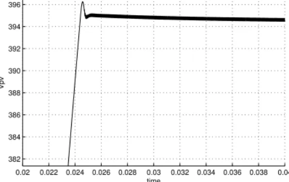
Fig. 18 shows the behavior of the PV array voltage vpvcontrolled with the voltage compensator designed in
section 3. Thevpvvoltage reaches the referenceVpv,ref=
394.5 V with zero steady state error. Fig. 19 shows the behavior of the PV array current.
5.2
DC-AC inverter
1)Control of the sinusoidal output currents - The simu-lation result presented in this section was obtained with the DC link capacitor replaced by a constant voltage source Vlink = 400 V. The objective is to analyze the
0.02 0.022 0.024 0.026 0.028 0.03 0.032 0.034 0.036 0.038 0.04 382
384 386 388 390 392 394 396
time
Vpv
Figure 18: Output voltage of the PV array and input voltage of the full-bridge DC-DC convertervpv.
0.02 0.022 0.024 0.026 0.028 0.03 0.032 0.034 0.036 0.038 0.04 13.8
13.9 14 14.1 14.2 14.3 14.4 14.5
time
Ipv
Figure 19: Output current of the PV array and input current of the full-bridge DC-DC converteripv.
Fig. 20 shows the three-phase currents synthesized by the current controller and injected into the grid through the three coupling inductors connected at the output of the DC-AC inverter (see to Fig. 8).
2)Control of the DC link voltage- The DC-AC converter was simulated separately from the rest of the system. As shown in Fig. 21, in this simulation the DC link capac-itorClinkis fed by a current source that is initially zero
and steps from 0 to 15A at t = 0.25 s. This simula-tion shows that the DC-AC converter and the voltage
0 0.002 0.004 0.006 0.008 0.01 0.012 0.014 0.016 0.018 0.02 −60
−40 −20 0 20 40 60
time
iabc
Figure 20: Three-phase currents injected into the grid.
Clink
vlink
iL
iin,inv ia,b,c
inverter
grid
+
−
Figure 21: Grid-connected DC-AC converter fed by a current source. iL= 0att <0.25 sandiL= 15A att >0.25s.
controller of Fig. 14 keep Clink charged at Vlink,ref. If
there is no energy source connected to the capacitor it is charged with energy from the AC grid. When the ca-pacitor is fed by the DC-DC converter (represented by the current sourceiL in this simulation) the capacitor is
charged with part of the input energy. The remainder of energy, that is not stored in the capacitor, is fully delivered as active power to the AC grid.
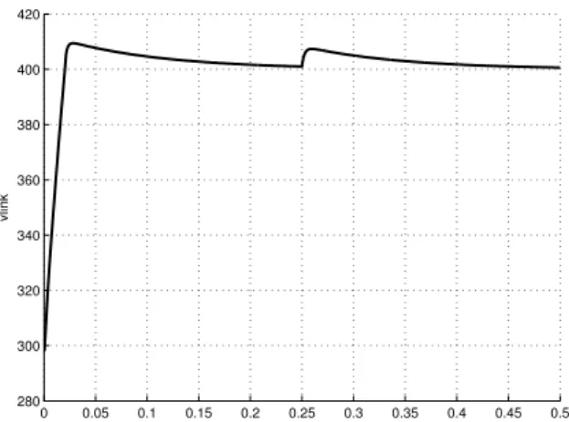
Figs. 22 and 23 show the DC link voltage and the output currents ia,b,c during this simulation. In Fig. 22 one
can see that the DC capacitor charges at the reference voltage of 400 V and after the current step the DC link voltage is reestablished by the voltage controller.
5.3
Complete system with DC and
DC-AC converters
In the preceding sections the DC-DC and DC-AC verters where individually simulated and the three con-trol systems (PV array voltage, DC link voltage and sinusoidal output currents) where individually analyzed without the influence of other system parts.
The objective of this section is to present the results of a simulation with all system parts working together: PV array, and DC-DC and DC-AC converters with their respective controllers.
It was shown in section 5.2 that the DC link voltage con-troller of Fig. 14 is capable to regulate thevlink voltage
even in the presence of a large step in the input current. It is now expected that the DC link voltage controller and the DC-AC converter will not significantly suffer influence from the DC-DC converter. Also, from the view point of the DC-DC converter, it is expected that the DC link voltage controller keeps the DC link voltage constant.
Fig. 24 shows the behavior of the DC link voltagevlink
and of the vpv during the simulation. The DC link
0 0.05 0.1 0.15 0.2 0.25 0.3 0.35 0.4 0.45 0.5 280
300 320 340 360 380 400 420
time
vlink
Figure 22: Plot of the DC link voltageVlink. The capacitor is
initially charged atVlink= 300V and there is no input current.
The capacitor is charged with energy from the AC grid until it reaches the reference voltage Vlink,ref = 400 V. The input
current of the converter (iL) steps from0to15 Aatt= 0.25 s.
drained from the AC grid at the system startup. In a practical system the DC link capacitor is charged either by a rectifier constituted of the DC-AC converter diodes, with a series resistance inserted before the capacitor only during the system startup, or by the DC-DC converter with output voltage control during the startup.
The PV output capacitor Cpv is charged from 0V to
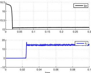
approximately 400 V with energy from the PV array. During the initial charge of the capacitor the PV ar-ray supplies its maximum current. Approximately near t = 0.25 s, when the capacitor is charged, the DC-DC converter starts to supply current (iL) to the DC-AC
converter, as Fig. 25 shows. The output sinusoidal cur-rents, that where draining power to charge the capacitor Clink, suffer a phase inversion near t= 0.25 s and from
this time the DC-AC converter begins to deliver active power to the grid, as Figs. 26 and 27 show.
6
EXPERIMENTAL RESULTS
This section shows some experimental results with the system operating at full load. At the time this paper was written the converter had not been tested with the PV plant and only laboratory experiments were available. The PV array was replaced by a high-power DC source in series with a 6 Ω resistance constituted by a bank of 36 halogen lamps. This experimental DC source permits to make all necessary tests with the converter before it is experimented with the real PV plant.
Fig. 28 shows waveforms of the system operating in steady state with approximately 8 kW of output power.
0 0.05 0.1 0.15 0.2 0.25 0.3 0.35 0.4 0.45 0.5 −40
−30 −20 −10 0 10 20 30 40
time
iabc
Figure 23: Three-phase output currents of the grid-connected converter. Fromt= 0 stot= 0.25 sthe system drains energy from the AC grid. From t = 0.25 s, when the input current steps from 0 to15 A, the converter injects active power into the grid.
0 0.01 0.02 0.03 0.04 0.05 0.06 0.07 0.08 0.09 0.1 0
50 100 150 200 250 300 350 400 450
time
Vpv Vlink
Figure 24: Plot of the DC link voltagevlinkand of the PV array
voltagevpv.
The DC link voltage was set at 500 V, the DC input is approximately 280 V and the input current is 35 A.
Fig. 29 shows the system behavior when submitted to a 6 kW power step. The DC input is suddenly connected and the system reaches steady state in 400 ms. The DC input is then removed and the system reaches again steady state (no output power) also in 400 ms (observing the DC link voltage perturbation). Fig. 30 shows the three-phase output currents and the DC link voltage in the same situation.
0 0.05 0.1 0.15 0.2 0.25 0.3 15
15.5 16 16.5
Ipv
0 0.02 0.04 0.06 0.08 0.1 −10
0 10 20
time
IL
Figure 25: Plot of the FB DC-DC output inductor currentiL
and of the PV array currentipv.
0 0.01 0.02 0.03 0.04 0.05 0.06 0.07 0.08 0.09 0.1 −40
−30 −20 −10 0 10 20 30
time
Ia,b,c
Figure 26: Output currentsia,b,c injected into the AC grid by
the DC-AC converter.
the most significant harmonic component (5 th). No noticeable 3 rd harmonic component is present and the subsequent components above the 5 th are very attenu-ated.
7
CONCLUSIONS
This paper has presented the modeling and control de-sign of a two-stage PV system based on a DC-DC full-bridge converter and a three-phase grid connected DC-AC inverter. The main objective of the paper was to de-velop small-signal models and design PI compensators for three purposes: the regulation of the PV voltage, the regulation of the DC link voltage and the injection of purely sinusoidal and synchronized currents into the grid. The simulation results and the experimental
re-0 0.01 0.02 0.03 0.04 0.05 0.06 0.07 0.08 0.09 0.1 −10000
−8000 −6000 −4000 −2000 0 2000 4000 6000 8000
time
Ppv Pout
Figure 27: Output power of the PV array and output power of the converter system delivered to the AC grid.
Figure 28: System at full load in steady state. In this order: Ch3 - DC link voltage (500 V/div); Ch2 - Output current of one phase (20 A/div); Ch1 - DC input current (50 A/div); Ch4 - DC input voltage (250 V/div).
Figure 30: System behavior with 6 kW power step. In this order: Ch1, Ch2, Ch3 - Output currents (20 A/div); Ch4 - DC link voltage (500 V/div).
Figure 31: Output current of one phase superimposed with the current reference (25 A/div).
Figure 32: FFT of the output current.
sults show that the objectives were successfully achieved. Besides presenting the subject of small-signal modeling of the input-regulated DC-DC converter, the paper also serves as a tutorial for the design of the system and several important subjects are carefully analysed: con-verter modeling, synchronous reference frame current controller, capacitor voltage controller, PV voltage reg-ulation, PLL and implementation of digital anti-windup PI compensators.
APPENDIX 1 - COORDINATE
TRANS-FORMATIONS
iα iβ
=
r
2 3
1 −1/2 −1/2 0 √3/2 −√3/2
ia ib ic
(28)
id iq
=
cosθ sinθ
−sinθ cosθ iα iβ
(29)
iα iβ
=
cosθ −sinθ sinθ cosθ
id iq
(30)
ia ib ic
= r
2 3
1 0
−1/2 √3/2 −1/2 −√3/2
iα iβ
(31)
APPENDIX 2 - DIGITAL THREE-PHASE
PLL
The digital PLL of Fig. 33 is a simplified version of the PLL presented in (Maraf˜ao et al., 2005) (Kubo et al., 2006) (Maraf˜ao et al., 2004). The principle of operation is the dot product between the voltage vec-tor v and the orthogonal vector u⊥. When the PLL
is synchronized with the grid voltages the two vectors are orthogonal and the product is zero. The PI com-pensator works to minimize the error ε = 0−v·u⊥,
i.e. to cancel the dot product, and generates the cor-rection component ∆ω. The integration of the angular frequencyω= ∆ω+ω0gives the angleθ⊥. The vectoru1
PI
v= [vsanvsbnvscn]
u⊥=
sin(θ⊥) sin(θ⊥−2π/3) sin(θ⊥+ 2π/3)
u1=
sin(θ1) sin(θ1−2π/3) sin(θ1+ 2π/3)
v·u⊥
θ1
θ⊥
θ⊥ integrator
ω0 ∆ω
+ + +
+ +
−
ε
0
u1
u⊥
π/2
Figure 33: Digital phase-locked loop.
APPENDIX 3 - IMPLEMENTATION OF
DIGITAL PI COMPENSATORS
The continuous-time compensators designed in previous sections can be realized as discrete-time digital com-pensators. There are several ways of discretizing ana-log compensators. All of them present similar results when the compensator bandwidth is not greater than 10% of the sampling frequency (Franklin et al., 1995). The Tustin or bilinear transform is used in this work. The compensators and controllers were implemented with the Texas floating point digital signal controller TMS320F28335 with sampling frequencyfs = 1/Ts = 10 kHz.
A discrete-time compensator is a digital filter. The filter coefficients may be obtained from the s-domain trans-fer function with the desired transformation method. In MATLAB the following command may be used to find the filter coefficients: [numz, denz] = bilinear(nums, dens, fs), where numz = [b0b1] and denz= [a0 a1] are
the numerator and denominator vectors with the coeffi-cients of the Tustin (or bilinear) approximation.
In the IIR direct transposed form the filter difference equation is (Oppenheim e Schafer, 1989):
yk =b0ek+b1ek−1−a1yk−1 (32)
The difference equation (32) is the simplest way to im-plement the PI compensator. The proportional and inte-gral components are embedded in the equation. In order to implement the simple anti-windup strategy proposed in this paper, one wish to develop another equation.
The following equation describes a PI compensator:
yk =kpek+kiik (33)
with the trapezoidal integratorik:
ik= Ts
2 [ek+ek−1] +ik−1 (34)
The compensator of (33) and (34) is equivalent to the compensator described by (32), with the difference that in (33) the proportional and integral parts are separated.
One can write the past integrator valueik−1 as:
ik−1= 1
ki yk−
kp ki
ek−1 (35)
soik can be rewritten as:
ik = kiTs
2 ek+ kiTs
2 ek−1+yk−1−kpek−1 (36)
Replacing (36) in (33), the difference equation (32) be-comes:
yk =
kp+
kiTs 2
| {z }
b0
ek+
kiTs
2 −kp
| {z }
b1
ek−1+yk−1 (37)
The above equation (37) shows the correspondence be-tween the coefficients of (33) and (32), with a1 = −1.
The difference equations (33) and (32) may be used in-distinctly to implement the first order PI compensator. However, in the form of (33) the simple anti-windup al-gorithm of Fig. 34 is possible. This alal-gorithm simply stops the integrator when the control output exceeds the limits. In practical systems the compensator output may sometimes exceed the maximum effective control ef-fort. This causes integrator saturation and deteriorates the control performance.
ACKNOWLEDGMENTS
This work was sponsored by FAPESP, CNPq, and CAPES.
REFERENCES
grid-ik=Ts
2[ek−1+ek−1] +ik−1
yk=kpek+kiik
(yk> ymax)||(yk< ymin)
ik=ik−1
yk=kpek+kiik
ek
yk
yes no
ek−1=ek
yk−1=yk
ik−1=ik
Figure 34: PI compensator with integrator anti-windup.
connected DC-AC converters with load power fac-tor correction,Generation, Transmission and Dis-tribution, IEE Proceedings-, Vol. 145, pp. 487–491.
Buso, S. e Mattavelli, P. (2006).Digital control in power electronics, Morgan & Claypool Publishers.
de Souza, K. C. A., Coelho, R. F. e Martins, D. C. (2007). Proposta de um sistema fotovoltaico de dois est´agios conectado `a rede el´etrica comercial, Re-vista Eletrˆonica de Potˆencia (SOBRAEP), Brazil-ian Journal of Power Electronics12(2): 129–136.
Erickson, R. W. e Maksimovic, D. (2001).Fundamentals of Power Electronics, Kluwer Academic Publishers.
Franklin, G. F., Powell, J. D. e Emami-Naeini, A. (1995). Feedback control of dynamic systems.
Kubo, M. M., Villalva, M. G., Maraf˜ao, F. P. e Rup-pert F., E. (2006). An´alise e projeto de PLL de desempenho melhorado baseado em filtro passa-baixas chebyshev inverso, 16th Brazilian Confer-ence on Automatic Control, CBA.
Kyocera (n.d.). KC200GT high efficiency multicrystal photovoltaic module (datasheet).
Maraf˜ao, F. P., Deckmann, S. M., Pomilio, J. A. e Machado, R. Q. (2004). A software-based PLL model: Analysis and applications.,Congresso
Brasileiro de Autom´atica, CBA, Brazilian Confer-ence of Control and Automation.
Maraf˜ao, F. P., Deckmann, S. M., Pomilio, J. A. e Machado, R. Q. (2005). Metodologia de projeto e an´alise de algoritmos de sincronismo PLL,Revista da Sociedade Brasileira de Eletrˆonica de Potˆencia (SOBRAEP), Brazilian Journal of Power Electron-ics10(1).
Middlebrook, R. (1988). Small-signal modeling of pulse-width modulated switched-mode power converters, Proceedings of the IEEE76(4): 343–354.
Middlebrook, R. D. e Cuk, S. (1976). A general unified approach to modelling switching converter power stage,IEEE Power Electronics Specialists Confer-ence, pp. 18–34.
Oppenheim, A. V. e Schafer, R. (1989). Discrete-Time Signal Processing.
Villalva, M. G., Gazoli, J. R. e Ruppert F., E. (2009a). Comprehensive approach to modeling and simula-tion of photovoltaic arrays,IEEE Transactions on Power Electronics25(5): 1198–1208.
Villalva, M. G., Gazoli, J. R. e Ruppert F., E. (2009b). Modeling and circuit-based simulation of photo-voltaic arrays,Revista Eletrˆonica de Potˆencia (SO-BRAEP), Brazilian Journal of Power Electronics.
Villalva, M. G. e Ruppert F., E. (2007). Buck con-verter with variable input voltage for photovoltaic applications,Congresso Brasileiro de Eletrˆonica de Potˆencia (COBEP).
Villalva, M. G. e Ruppert F., E. (2008a). Dynamic anal-ysis of the input-controlled buck converter fed by a photovoltaic array,Revista Controle & Automa¸c˜ao - Sociedade Brasileira de Autom´atica, Brazilian Journal of Control and Automation19(4): 463–474.