Design and Implementation of 12V/24V Closed
loop Boost Converter for Solar Powered LED
Lighting System
P.Sathya1, Dr.R.Natarajan 2
1
Assistant Professor, School of Electronics Engineering, VIT University, Vellore, Tamil Nadu, India 2
Professor, School of Mechanical and Building Sciences, VIT University, Vellore, Tamil Nadu, India 1
p.sathya@vit.ac.in 2
rnatarajan@vit.ac.in
Abstract— this paper presents the design and implementation of high performance closed loop Boost
converter for solar powered HBLED lighting system. The proposed system consists of solar photovoltaic module, a closed loop boost converter and LED lighting module. The closed loop boost converter is used to convert a low level dc input voltage from solar PV module to a high level dc voltage required for the load. To regulate the output of the converter, closed loop voltage feedback technique is used. The feedback voltage is compared with a reference voltage and a control signal is generated and amplified. The amplified signal is fed to 555 Timer which in turn generates a PWM signal which controls the switching of MOSFET. Thus by switching of MOSFET it would try to keep output as constant. Initially the boost converter, timer circuit, amplifier circuit and LED light circuits are designed, simulated and finally implemented in printed circuit board. The simulation studies are carried out in MULTISIM. The experimental results for solar PV and boost converter obtained in both software and hardware are presented here.
Keywords- Solar Photovoltaic (SPV), PWM, boost converter, MOSFET switching, HBLED light
I. INTRODUCTION
Renewable energy sources play an important role in electricity generation. People are finding the benefits of having their own renewable energy system more attractive than they ever had before. Specially, energy from the sun is the best option for electricity generation as it is available everywhere and is free to harness. The merits of solar PV system are cleanness, relative lack of noise or movement, as well as their ease of installation and integration when compared to others. On an average the sunshine hour in India is about 6hrs annually also the sun shine shines in India for about 9 months in a year. Electricity from the sun can be generated through the solar photovoltaic modules (SPV). The SPV comes in various power output to meet the load. However, the output power of a PV panel is largely determined by the solar irradiation and the temperature of the panel. At a certain weather condition, the output power of a PV panel depends on the terminal voltage of the system. To maximize the power output of the PV system, a high efficiency, low-cost DC/DC converter with a voltage feedback signal is commonly employed to control the terminal voltage of the PV system at optimal values in various solar radiation conditions.
Lighting is an essential requirement for any facility and to carry out our daily work round the clock. LED light consumes very less power and its life time is also high. Hence, in this project to conserve energy HBLED lights are used along with electric power generation using solar PV.
II. REVIEW OF LITERATURE
Literature collected from different journals, conference papers and books has been reviewed as follows. A boost converter is designed to step up a fluctuating or variable input voltage to a constant output voltage of 24 volts with input range of 6-23volts in [1]. To produce a constant output voltage feedback loop is used. The output voltage is compared with a reference voltage and a PWM wave is generated, here PIC16F877 microcontroller is used to generate PWM signal to control switching action.
A DC to DC converter is used to step up from 12V to 24V in [2]. The 12V input voltage is from the battery storage equipment and the 24V output voltage serves as the input of the inverter in solar electric system. In designing process, the switching frequency, f is set at 20 kHz and the duty cycle, D is 50%. The tool that has been used for circuit simulation and validation are National Instrument Multisim and OrCAD software.
The output of the boost converter is tracked, measured continuously and the values are sent to the microcontroller unit to produce pulse-width-modulation (PWM) signal. The PWM signal is used to control the duty cycle of the boost converter. Typical application of this boost converter is to provide DC power supply for inverter either for grid-connected or standalone system. Simulation and experimental results describe the performance of the proposed design. Microcontroller PIC16F877 is used to perform tasks in the proposed design.
This paper concerns with design and simulation of DC/DC boost converter to operate in PV system [4]. The system has a nonlinear dynamic behavior, as it work in switch-mode. Moreover, it is exposed to significant variations which may take this system away from nominal conditions, due to changes on the load or on the line voltage at the input. The input is obtained by PV array. In this paper the equations of a boost converter are analyzed and a design components and simulation of DC/DC boost converter is proposed. Here simple design equations are used to design the components value in different modes as CCM and DCM and simulation is done in simulink.
From the literature review it is found that mostly microcontrollers are used for generating PWM signal to perform switching control action. In this project a simple approach is used to generate the PWM signal with high accuracy and less cost. To improve the output power of solar PV panel a low cost DC/DC closed loop boost converter is designed. The load used is high brightness white LED which has many advantages like long life span, speed of response, high efficacy, less power consumption and high directionality. The performance the whole system is verified by simulation in NI-Multisim (version-11) and then implemented in hardware.
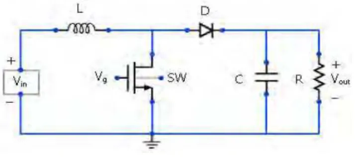
III. THE PROPOSED SYSTEM
Fig. 1 Block diagram of the proposed system
The block diagram shown above consists of a PV panel, dc-dc boost converter and LED lights as load. The proposed standalone PV controller implementation takes into account mathematical model of each component as well as actual component specification. The dc–dc converter is the front-end component connected between the PV array and the load.
Solar PV Panel:
The PV array which we used is made up of mono-crystalline fiber. It has two layer one is very thick and another is very thin. The array used here contains thick n layer. An array contains 36 cells and each cell can produce maximum of 0.5 volts thus maximum of 18 volts can be extracted from a PV panel. The output of the array varies from 12 to 18 volts for different values of load. The used solar panel is shown in Fig.2.
Fig. 2 Various parts of the solar panel used for the project
DC-DC Boost Converter:
for a period of time (usually in the 20 kHz to 5 MHz range) which causes current to flow through it and store energy magnetically, then switching this voltage off and causing the stored energy to be transferred to the voltage output in a controlled manner. The output voltage is regulated by adjusting the ratio of on/off time. This is achieved using switched-mode, or chopper, circuits whose elements dissipate negligible power. Pulse-width modulation (PWM) allows control and regulation of the total output voltage. It is considered as the heart of the power supply, thus it will affect the overall performance of the power supply system. The ideal converter exhibits 100% efficiency; in practice, efficiencies of 70% to 95% are typically obtained.
Fig. 3 Schematic of Boost converter
The dc-dc boost converter shown in fig.3 is operated in two modes.
Mode-1: When the MOSFET switch is in ON state (closed), the whole circuit will be divided into two loops one at the output side and another at the input side. The closed loop at input consisting of inductor gets charged by the current flowing through the loop during this period. This current will increase linearly till the time the switch is in closed condition. In the same time interval, inductor voltage is also high as it is not delivered to any load but to itself. Diode is off during this mode. The equivalent circuit representation of mode 1 is shown in fig.4.
Fig. 4 Equivalent circuit of mode 1
Mode-2: When the switch is in OFF state (Open), there will be a closed loop consisting of power source, inductor and RC load. The energy stored in the inductor during ON state is discharged to the RC load circuit through the diode. Thus inductor current is reducing linearly, charging the capacitor at the load side. The equivalent circuit for mode 2 is shown in fig.5.
Fig. 5 Equivalent circuit of mode 2
IV. DESIGN APPROACH
Load Requirement:
The load is a simple 4 x 4 LED panel andeach row containing 4 LED in a line would require a current of 10-15 mA and thus total of 60 mA to all four branches and thus having a resistance of 570Ω. As each LED gives a drop of 2.1 volts to become forward biased, so a minimum of 8.4 volts is required to glow 4 LED in series, for this a voltage of 24 V is required to be supplied to LEDs. Thus the load requirement is 570 Ω with 42 mA of total current thus required voltage was 24 V. Since a potential divider is used whose total resistance is 1100Ω so total equivalent resistance is Req = (1100) ││ (570) = 375Ω.Based on this load requirement the other parameters would be calculated and the specifications are tabulated in the following table.
TABLE I Specifications
Duty Cycle:
The duty cycle can be found using the following relation
Inductor value:
The value of inductor is determined using the following relation
An inductor is practically designed using the following parameters and is shown in the figure 6. Formula for inductor design, L = (d2n2) / (l + 0.45d)
Required dimensions of inductor Coil length, l= 8.1 cm
Diameter, d= 6.3 cm
Inductance value required, L= 151 µH Number of turns, n=64
Where L is inductance in micro Henrys, d is coil diameter in meters,
l is coil length in meters, and n is number of turns
Fig.6 Practically designed Inductor
Capacitor value:
The value of capacitor is determined from the following equation
Where
PARAMETER VALUE UNIT
Input voltage, Vin 10-18 Volts
Output voltage, Vout 24 Volts
C is the minimum value of capacitance,
D is duty cycle,
R is output resistance,
Fs is switching frequency, and
Vr is output voltage ripple factor.
Design of differential amplifier:
A differential amplifier is designed using µA741 with a gain of 100. Input to the non inverting terminal is fixed equal to 9 percent of expected output and inverting terminal input other is taken from the potential divider of boost converter. The difference between these two is amplified with a gain of 100 and the circuit is shown in figure 7.
Fig.7 Differential amplifier
Design of PWM Generator:
The output of differential amplifier is fed to 555 Timer which in turn generates PWM signal. The PWM signal required for switching action is with a frequency of 219 KHz and duty ratio of 50 percent. To generate a 50 percent duty cycle, the 555 timer has to work in astable mode. By connecting diode, D1 between the trigger input and the discharge input, the timing capacitor would charge up directly through resistor R1 only, as resistor R2 is effectively shorted out by the diode. The capacitor discharges as normal through resistor, R2. The previous charging time of t1 = 0.693(R1 + R2) C is modified to take account of this new charging circuit and is given as: 0.693(R1.C). The duty cycle is therefore given as D = R1 / (R1 + R2). Then to generate a duty cycle of more than 50%, resistor R1 needs to be equal to resistor R2.
Fig.8 PWM Generator
Selection of components for Hardware implementation:
A. Selection of Electronic Switch
The electronic switch (Power MOSFET) is chosen based on its voltage and current rating which have to be higher than the maximum input voltage and current.
B. Selection of Inductor
The minimum inductance for boostconverter to operate in continuous conduction mode is given in equation. Therefore the selection of the inductor should be higher thanthe calculated value.
Diode reverse voltage rating is the main consideration for selecting the diode. Other important consideration is its ability to block the required off–state voltage stress and to have sufficient peak and average current handling capability, fast switching characteristics, low reverse–recovery, and low forward voltage drop.
D. Selection of Output Capacitor
The minimum capacitance for calculating ripple voltage is given above. The selection of capacitor is higher than the calculated value. Another important consideration is its equivalent series resistance, ESR. Since the capacitor’s ESR affects efficiency, low-ESR capacitors could be used for best performance. ESR could be reduced by connecting few capacitors in parallel.
V. EXPERIMENTAL SET UP
A. PV array output measurement:
Fig. 9 Circuit diagram to find I-V and P-V curve.
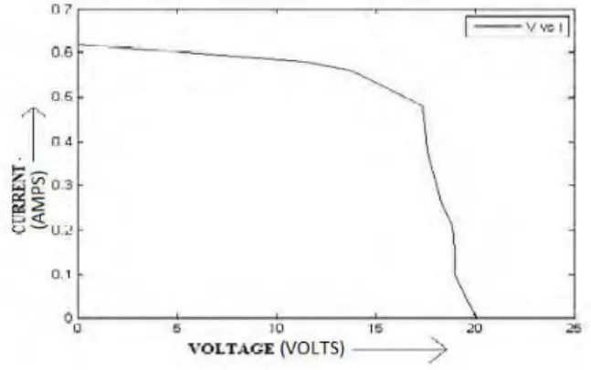
The experimental set up of solar PV module to test the I-V and P-V characteristics is shown in fig.9. In order to find various current – voltage points of the PV module, a rheostat is used as load. Before proceeding the experiment, the open circuit voltage and short circuit current of the PV module is measured. The open circuit voltage is the voltage that is output to the cell terminals when the cell is exposed to light and there is no current flowing between the terminals. This is also the maximum voltage that can be produced by the cell, which makes knowing this number useful when designing a circuit or load to connect to the cell terminals. The short circuit current is the current that will flow when the cell is under light and the terminals are shorted together. This is the maximum current that can be output by the specific solar cell. Each individual cell is relatively little in size and can only produce a small amount of power. The Voc of an individual solar cell is usually approximately 0.6 V. The cells become much more useful when combined in an array to create a PV panel. When connected together the cells properties add together to create an I-V curve that has the same appearance as that of an individual cell but is larger in magnitude. The cells in an array are usually connected in series to obtain a higher and more appropriate terminal voltage. The values obtained are shown in table II.
TABLE II Solar PV Output Values
VOLTAGE (V) CURRENT (A) POWER (W)
20.1(open circuit) 0 0
0 0.62(short circuit) 0 11.4 0.58 6.612 13.8 0.56 7.728 17.4 0.48 8.352 17.6 0.38 6.688 18.3 0.26 4.758 18.9 0.21 3.969
The corresponding characteristic graphs drawn are shown below in figure 10 and 11.
Fig. 10 I-V characteristics of solar PV module
Fig. 11 P-V characteristics of solar PV module
B. Simulation of Experimental setup
Fig. 12 DC/DC Boost converter with HBLED lighting load
timer is fed to the gate terminal of the power MOSFET. This pulse in turn will control the switching of the MOSFET based on its switching frequency; here it is designed for a switching frequency of 219 kHz. Thus when pulse is at high level the MOSFET would be in saturation mode there by making switch ON condition. When pulse is at low level the MOSFET would be in cutoff mode of operation and thereby making switch open i.e. switch OFF condition. Whenever input to converter becomes low the output also becomes low and duty cycle gets increased and tries to keep output constant. When input to converter increases the output increases and duty cycle of timer decreases and tries to bring output at the previous level. Thus closed loop operation regulated the output voltage against the variations in input voltage ranging from 10 to 18 volts.
C.Analysis of Circuit and Result:
Analysis of the circuit is carried out based on the following assumptions. The circuit is ideal. It means when the switch is ON, the drop across it is zero and the current through it is zero when it is open. The diode has zero voltages drop in theconducting state and zero current in the reverse-bias mode. The time delays in switching on and off the switch and the diode are assumed to be negligible. The inductor and the capacitor are assumed to be lossless.
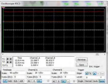
The responses in the circuit are periodic. It means especially that the inductor current is periodic. Its value at the start and end of a switching cycle is the same. The net increase in inductor current over a cycle is zero. If it is non-zero, it would mean that the average inductor current should either be gradually increasing or decreasing and then the inductor current is in a transient state and has not become periodic.The voltage across the inductor and linear variation of current through inductor are shown in figure 13.
Fig.13 Waveform of Inductor current and Inductor voltage
It is assumed that the switch is made ON and OFF at a fixed frequency and let the period corresponding to the switching frequency is T. Given that the duty cycle is D, the switch is on for a period equal to DT, and the switch is off for a time interval equal to (1 - D)T. The inductor current is continuous and is greater than zero. Here the triangular waveform is inductor current and square waveform is voltage across inductor.
The capacitor is relatively large. The RC time constant is so large, that the changes in capacitor voltage when the switch is ON or OFF can be neglected for calculating the change in inductor current and the average output voltage. The average output voltage is assumed to remain steady, excepting when the change in output voltage is calculated.
Fig.14 Waveform of output current and voltage
D.Hardware Implementation:
The complete closed loop boost converter with LED lighting load is developed as hardware in real time. The experimental setup consisting of input from solar PV module, closed loop dc/dc converter and HBLED lighting load is tested in the ZealTech work bench. The work bench consists of embedded power supply units, ac and dc meters for measuring current and voltage, signal generator and cathode ray oscilloscope. The hardware is tested at various levels for a given input voltage variation. The observed results in both hardware and software simulation are compared and shown in table III. The expected output is 24 volts and in software it is coming 23.6 volts while in hardware it is getting regulated to 22.76 volts.
TABLE III
Closed Loop Boost Converter Output
Vin (Volts) Vout (Volts)
(Simulation)
Vout ( Volts)
(Hardware)
10 23.6 22.46
11 23.6 22.77
12 23.6 22.80
13 23.6 22.81
14 23.6 22.80
15 23.6 22.80
16 23.6 22.79
17 23.6 22.81
Fig.15 PCB view of Boost Converter and load in Multisim
Fig.16 Prototype Board
VI. CONCLUSION
In this paper a low cost high performance DC-DC closed loop boost converter has been proposed. The proposed system used solar PV as the input and HBLED as the output which conserves the power. The complete system has been designed and simulated in Multisim which resulted in an efficiency of 98.33%. A laboratory prototype board has been built and experimentally tested for the input voltage ranging from (10-18)V. For the specified input variation, a regulated dc output voltage of 22.76V has been obtained resulting in an efficiency of 95%.
REFERENCES
[1] S. Masri and P. W. Chan, “Design and development of a dc-dc Boost converter with constant output voltage”, IEEE, International conference on Intelligent and Advanced systems (ICIAS), June 2010.
[2] Asmarashid Ponniran and Abdul Fatah Mat Said.,“DC-DC Boost Converter Design for Solar Electric System”, International conference on Instrumentation, Control and Automation, October 20-22 (ICA 2009) Bandung.
[3] Syafrudin Masri and Pui-Weng Chan, “Development of a Microcontroller-Based Boost Converter for Photovoltaic System”, European Journal of Scientific Research. ISSN 1450-216XVol.41No.1,pp.38-47. http://www.eurojournals.com/ejsr.htm
[4] Diary R. Sulaiman, Hilmi F. Amin, and Ismail K. Said., “Design of High Efficiency DC-DC Converter for Photovoltaic Solar Home applications”, Journal of Energy and Power engineering, 2009.
[5] Muhammad H. Rashid, Power Electronics Circuits, Devices, And Applications, 3rd edition, University of West Florida, Pearson Prentice Hall, 2003.