High Voltage Coil Current Sensor
for DC-DC Converters Employing DDCC
Martin DRINOVSKY
1,2, Jiri HOSPODKA
11Dept. of Circuit Theory, Czech Technical University in Prague, Technická 2, 166 27 Praha, Czech Republic
2STMicroelectronics Design and Application s.r.o., Pobřežní 620/3, 186 00 Praha, Czech Republic
[email protected], [email protected]
Abstract. Current sensor is an integral part of every switching converter. It is used for over-current protection, regulation and in case of multiphase converters for balanc-ing. A new high voltage current sensor for coil-based current sensing in DC-DC converters is presented. The sensor em-ploys DDCC with high voltage input stage and gain trimming. The circuit has been simulated and implemented in0.35µm
BCD technology as part of a multiphase DC-DC converter where its function has been verified. The circuit is able to sus-tain common mode voltage on the input up to40V, it occupies
0.387×0.345mm2and consumes3.2mW typically.
Keywords
Current sensor, current conveyor, DDCC, DC-DC con-verter
1. Introduction
The switching converters have become an important part of nearly every electronic system, such as mobile phones, tablets or computers. One of the widely used switching con-verter topology is the buck concon-verter used for converting high input voltage into a lower output voltage. The buck converter uses a coil to transfer current from the input to the output. This current is often measured for various purposes, e.g. for over-current protection or for regulation when a current con-trol loop is employed.
Several approaches for current sensing exist [1-2]. When the power MOS transistors are integrated on-chip the copy or sense MOS technique is used [3-5]. For applications with off chip power transistors other techniques measuring coil current must be used.
One way of measuring coil current uses a sensing resis-tor in series with the coil as depicted in Fig. 1a. This has the disadvantage of introducing additional loss into the system and lowering overall efficiency. Other method uses the para-sitic resistance of the coil (DCR) to measure the current [1]. This is done by adding a filter in parallel to the coil as shown
in Fig. 1b, whereRLrepresents a DC resistance of the coil.
If the following condition holds
RC= L RL
, (1)
then the voltage on the capacitor is proportional to the induc-tor current as
vC(t)=RLiL(t). (2)
(a)
R
RL L
Vsense C
Vout
VIN
Drivers
M2 M1
Vout
(b)
Rsense
L Vout
M1
M2
Drivers
VIN
Vout
Vsense
Fig. 1.Coil current sensing: (a) On external resistor and (b)
filter-based sensing on coil resistance.
One of the circuits sensing coil current is presented in [6], this solution cannot be used for high voltage sens-ing as it is limited by the capability of the standard voltage components. The sensing circuit presented in [7] requires an operational amplifier with both high voltage input and output. This complicates design because all the basic structures must be cascoded with high voltage components. The same prin-ciple is also used in [8], where the current sensors uses the current shunt monitor chip INA139. The circuit in [9] uses instrumentation amplifier to sense the coil current, however it still requires high voltage operational amplifiers. Another solution [10] uses capacitors to sample the input voltage but it requires capacitors with high voltage capability available in the given process.
In this paper a novel current sensor with high voltage input is presented. It is based around a differential-difference current conveyor (DDCC) with only one input stage with
9*12/3 VDD
M12
M14
60 uA typ.
HV M36 M35HV HVM34 M33 HV HVM6 HV M5 X REF N P 10 uA 60 uA
80 uA 80 uA 90 uA
Ioff = 100 uA 5*30/6 2*30/6M29 50/2.2 M31HV VIN Idiffp 20/2.2 4*8/6 4*8/6M39 10/2.2 10/2.2 10 uA M44 M43 VDD HV M40 VIN M4 M3 M2 M1 10 uA ratio 2:5 M38 M37 M32 M30 M28 M27 Z2 Z1 VDD M26 M25 VDD M24 M20 M19 M18 M17 M16 M15 M13 M11 M10 M9 M8 M7 VDD N P HV HV
VIN VIN VDD VDD VDD
Cc
5 uA
bias1
bias2
8*20/2 8*20/2 8*20/2 8*20/2
200/2.2 200/2.2 200/2.2 20/2.2 10/2.2 10/2.2 10 uA 8*20/6
20/6 8*20/6 9*20/6 6*20/6
4/1 8*4/1 8*4/1 9*4/1 6*4/1
M23
4*15/3 4*15/3 4*15/3
10*4/1 10*4/1 10*4/1
2*20/1 M22 M21 M41 M42 8*1/0.8 8*1/0.8 10*1/0.8 1/0.8 10*12/3 12/3 11*12/3 11*12/3
Fig. 2.Schematic of the proposed DDCC based current sensor (dimension are inµm).
high voltage requirements thereby reducing the number of high voltage components, area and design effort. The circuit description is presented in Sec. 2, achieved results can be found in Sec. 3 and conclusion follows in Sec. 4.
2. Proposed Circuit
The block diagram of the proposed current sensor is shown in Fig. 3. The basic building block is the DDCC [11] with multiple outputs which is described in ideal form as
IREF=0,IP=0,IN =0, (3a)
VX =VREF+α(VP−VN), (3b)
IZ1 =IZ2 =IX−Ioff, (3c)
whereIoffis internally added offset current to allow simple
bidirectional signal processing by the subsequent circuitry
and the gainαequals 1 for a traditional DDCC. The detailed
analysis of the DDCC behaviour has been carried in [11]. For
accurateαthe internal feedback loop must have a sufficient
gain, this is guaranteed by cascoding of the current mirrors. Another major source of inaccuracy are the nonlinearities of the transconductance stages. These lead to complex expres-sions with little insight, however, for the given application they are tolerable as will be shown in the simulation results.
The sensed voltage difference on theRsenseis copied by
the DDCC onto a resistorRcopy, therefore the output currents
are proportional to the coil current as
IZ1,2=αIL
Rsense
Rcopy −Ioff. (4)
The output currents are identical and can be easily added and scaled according to the various needs of the
applica-tion. TheVbiasis a constant inaccurate voltage selected in the
common mode range of the inputs. To save the application
board space and reduce component count the resistor Rcopy
is implemented on-chip. However, the technological spread of the resistor leads to the inaccuracy of the gain. This is
compensated by trimming the gain α as will be described
further. Vbias Rsense L Ix Iz2 Iz1 Iref In Ip to current sharing comparator to OCP Rcopy Vout M1 M2
− HV −
DDCC REF X P N Z1 Z2 Drivers VIN
Fig. 3.Block diagram of the proposed DDCC based current
sen-sor.
The schematic of the proposed DDCC can be found in Fig. 2. The circuit employs two
3.3 V differential pairs denoted as high voltage (HV) and low voltage (LV) owing to the voltage levels they are process-ing. The HV pair is composed of transistor M1-M2 and the LV pair is composed of transistors M3-M4. The current from the two differential pairs is summed by the folded cascode (M7-M8, M10-M15) followed by a second gain stage (M9, M16-M17), voltage follower M20 completes the feedback loop around the low voltage differential pair. The current mirrors M23-M28 copy the current through terminal X to the outputs Z1 and Z2. Current source M21-M22 adds an
offset currentIofffor bidirectional operation.
The M33-M35 form a differential pair with M33 and M34 averaging the input voltage.
The transfer of the voltage from the HV input pair to
the nodeX is given by the ratio of the transconductances of
the two differential pairs, i.e.
α=g H V m
gmLV
= g
M1 m
gmM3
. (5)
The mismatch between the two differential pairs and their bias current will cause mismatch between the two transcon-ductances. This together with the process variations of the
internal resistorRcopywill lead to the gain inaccuracy. Both
of these effects can be trimmed by using the relation forα
and trimming the transconductance of the HV stage. This is done by varying the bias current of the HV stage since to a first degree the transconductance is proportional to the bias current [12]. The bias current is set by the gain trimming DAC and mirrored by the HV current mirror M29-M32.
The gain trimming DAC is depicted in Fig. 4.
1uA
16
16 8
8 4
4 2
2 1
1
1 1
l=1u
l=15u l=800n w=5u w=24u
w=4.2u
Iout
24 uA typ.
trimming range 16 uA − 31 uA
16uA 8uA
4uA 2uA
MSB LSB
1uA
HV HV HV HV HV
b0 b1 b2 b3 VDD
Ibias
Fig. 4.Gain trimming DAC (dimensions apply for entire rows).
It is based on binary scaled current sources with added offset
current. The typical current value is 24µA with a trimming
range spanning from 16µA to 31µA.
3. Implementation and Results
The proposed current sensor was realized in 0.35 µm
BCD technology from STMicroelectronics. The area of the
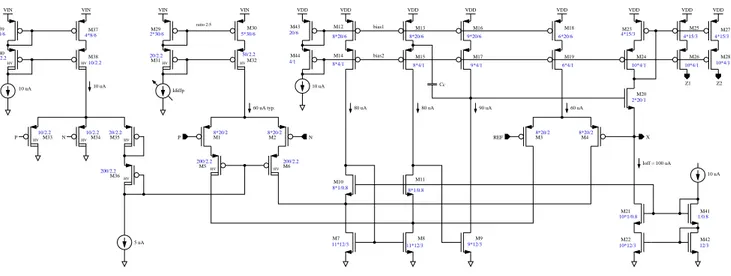
current sensor is 0.387×0.345 mm2as can be seen in Fig. 5.
The LV part is supplied from an on-chip 3.3 V regulator
whereas the HV part is supplied from the input voltage of the DC-DC converter which can go as high as 40 V. For a typical
input voltage of 12 V the circuit consumes 3.2 mW.
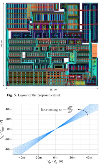
Fig. 6 shows the simulated transfer characteristics for different trimming combinations. The gain trimming range
is within±22 % with a step about 2.8 %. This is sufficient to
trim the process variation of the internal resistorRcopywhich
is the major contributor of the gain variation.
Fig. 5.Layout of the proposed circuit.
Fig. 6.Transfer characteristics.
Due to the nonlinear dependence ofgm onID the linearity
of the sensor deteriorates with the trimming going further from the default value. This can be seen on the nonlinearity characteristics in Fig. 7. However in the given application the input differential voltage usually does not exceed 20 mV for which the error caused by the nonlinear behaviour of the current sensor does not exceed 0.2 %.
0.0 0.4 0.8 1.2
-0.4
-0.8
0m 20m 40m
-20m -40m
Input differential voltage [V]
No
n
li
n
ea
ri
ty
[
%]
TRIMM_MAX
TRIMM_TYP
TRIMM_MIN
Fig. 7.Achieved nonlinearity(Isim/Iideal−1)for different trim-ming steps.
The AC gain and phase response from the input ter-minal to the X node are in Fig. 8. The bandwidth reaches
0
-10
-20
-30
-40
0
-40
-80
-120
-160
-200
-240
-280
-320
1m 1 1k 1M 1G
M
a
g
n
itu
d
e
[d
B]
Frequency [Hz]
Ph
a
s
e
[d
eg
]
Fig. 8.Gain and phase characteristics ofVX/Vsense.
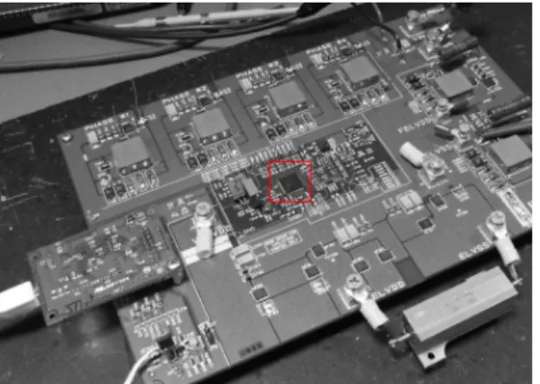
The proposed circuit was taped-out as part of a four-phase buck DC-DC converter whose application board is in Fig. 9. The output of the current sensor is used for over-current protection and for balancing the over-current evenly among all the phases. Although the current sensor could not be mea-sured directly the operation can be verified by the balancing function of the system, as shown in Fig. 10. The waveforms labeled IL1, IL2 and IL4 are coil currents corresponding to three of the phases and are sensed by the described circuit as in Fig. 3. The same average currents of the phases show correct operation of the circuit.
Fig. 9.Application board with the device (mark in square)
fea-turing the proposed current sensor.
Fig. 10.Output voltage and current of three phases balanced
with the help of the proposed sensor.
4. Conclusion
In this paper a new circuit for coil current sensing in high voltage DC-DC converters has been presented. A method for gain trimming based on transconductance variation of the input stage has been described.
The proposed solution has no static input current and the usage of high voltage components is limited to the in-put stage thereby reducing power consumption and silicon area. This is in contrast with traditional approaches, such as [7-9], where the operational amplifier has to be designed with both the input and output stages able to sustain high voltage. Another approach presented in [10] requires high voltage capacitors and the need for reset phase further com-plicates design and top-level integration. On the other hand, the presented sensor does not employ any special compo-nents but the standard CMOS and DMOS transistors present in any BCD type technology. Also the continuous operation simplifies integration with the rest of the application.
The circuit has been implemented in
STMicroelec-tronics 0.35 µm BCD technology and occupies area of
0.134 mm2. It has been integrated as part of a multi-phase
DC-DC converter and its function has been verified. The proposed solution is suitable for DC-DC converters with ex-ternal power MOS transistors where traditional sensors based on copy MOS transistors are not possible as one cannot ef-fectively match integrated transistors with external ones from a different lot or possibly a different technology.
Acknowledgments
The authors would like to thank STMicroelectronics for design fabrication and measurements. The work has been supported by the grant No. SGS12/143/OHK3/2T/13 of the CTU in Prague.
References
[1] PATEL, A., FERDOWSI, M. Current sensing for automotive electron-ics – a survey.IEEE Transactions on Vehicular Technology, 2009, vol. 58, no. 8, p. 4108–4119. DOI: 10.1109/TVT.2009.2022081
[2] FORGHANI-ZADEH, H. P., RINCON-MORA, G. A. Current-sensing techniques for DC-DC converters. InThe 2002 45th
Mid-west Symposium on Circuits and Systems (MWSCAS). 2002, vol. 2,
p. II-577–II-580. DOI: 10.1109/MWSCAS.2002.1186927
[3] DU, M., LEE, H. An integrated speed- and accuracy-enhanced CMOS current sensor with dynamically biased shunt feedback for current-mode buck regulators.IEEE Transactions on Circuits and
Systems I: Regular Papers, 2010, vol. 57, no. 10, p. 2804–2814. DOI:
10.1109/TCSI.2010.2046258
[4] LEE, C. F., MOK, K. T. A monolithic current-mode CMOS DC-DC converter with on-chip current-sensing technique.IEEE
Jour-nal of Solid-State Circuits, 2004, vol. 39, no. 1, p. 3–14. DOI:
[5] YUAN, B., LAI, X. On-chip CMOS current-sensing circuit for DC-DC buck converter.Electronics Letters, 2009, vol. 45, no. 2, p. 102– 103. DOI: 10.1049/el:20092855
[6] WANG, S. W., CHO, GYU-HA, CHO, GYU-HYEONG A high-stability emulated absolute current hysteretic control single-inductor 5-output switching DC-DC converter with energy sharing and balancing. In IEEE International Solid-State Circuits Conference
Digest of Technical Papers (ISSCC) 2012, p. 276–278. DOI:
10.1109/ISSCC.2012.6177002
[7] SUN, J., ZHOU, J., XU, M., LEE, F. C. A novel input-side current sensing method to achieve AVP for future VRs.IEEE Transactions
on Power Electronics, 2006, vol. 21, no. 5, p. 1235–1242. DOI:
10.1109/TPEL.2006.880347
[8] HWU, K. I., CHEN, Y. H. Current sharing control strategy based on phase link.IEEE Transactions on Industrial Electronics, 2012, vol. 59, no. 2, p. 701–713. DOI: 10.1109/TIE.2011.2151820
[9] SIMON-MUELA, A., PETIBON, S., ALONSO, C., CHAPTAL, J.-L. Practical implementation of a high-frequency current-sense technique for VRM.IEEE Transactions on Industrial Electronics, 2008, vol. 55, no. 9, p. 3221–3230. DOI: 10.1109/TIE.2008.927968
[10] WICHT, B., KULHARNI, S. P., HERZER, S., NEIDHARDT, J. Switched Mode Power Supply with Current Sensing, US Patent
8,203,323.June 19, 2012.
[11] CHIU, W., LIU, S.-I., TSAO, H.-W., CHEN, J.-J. CMOS differential difference current conveyors and their applications.IEE Proceedings – Circuits, Devices and Systems, 1996, vol. 143, no. 2, p. 91–96. DOI: 10.1049/ip-cds:19960223
[12] ENZ, C. C., KRUMMENACHER, F., VITTOZ, E. A. An analytical MOS transistor model valid in all regions of operation and dedicated to low-voltage and low-current applications.Analog Integrated
Cir-cuits and Signal Processing, 1995, vol. 8, no. 1, p. 83–114. DOI:
10.1007/BF01239381
About the Authors . . .
Martin DŘÍNOVSKÝ was born in 1985. He received his Master’s degree from the Czech Technical University in Prague and is currently studying towards Ph.D. at the Depart-ment of Circuit Theory. He is with STMicroelectronics since 2010 working as a senior design engineer. His research in-terests include analog and mixed-signal circuits, IP modeling and verification methodologies.