Brazilian Journal of Physics, vol. 29, no. 4, Dezembro, 1999 793
Impurity Breakdown in GaAs Samples
Grown by Molecular Beam Epitaxy
R.M.Rubinger,A.G. de Oliveira, G.M.Rib eiro,J.C. Bezerra,C.M. Silva,
W.N. Ro drigues, and M.V.B.Moreira
Departamento de Fisica, Universidade Federal de Minas Gerais CP702, 30123-970 Belo Horizonte, Brazil
Received February, 1999
In this work we present studies for the behavior of impurity breakdown of two GaAs samples grown by Molecular Beam Epitaxy at 200o
C and 300 o
C. We vary the temperature and the illumination
intensity. For the sample grown at 200o
C, the transport mechanism after the breakdown is of
the same type of the main free carriers at low electric elds. Below 100K, a clear dependence of the threshold electric eld with temperature was observed. The sample grown at 300o
C shows a
breakdown due to an acceptor level at 41meV from the valence band. The threshold electric eld increases with illumination due to the generation of free electrons by deep levels. A similar behavior was also observed for a Cr doped GaAs sample.
I Introduction
Negative dierential conductivity (NDC) has been studied since the early 60's. Basically it was studied with the intention to develop microwave devices for engineering applications. In the 80's, studies of non-linear dynamics and chaotic phenomena have started the development of a new class of semiconductor de-vices where nanostructures details should play impor-tant roles. We have studied the current-voltage (IxV) characteristics of GaAs samples grown by Molecular Beam Epitaxy (MBE) at low temperatures (LT). We have compared the results of two samples, one grown at 200o
C(sample BH9801) and other at 300 o
C(sample
BH9525). These results were also compared with those obtained from a standard commercial Cr-doped GaAs substrate. For the semi-insulating (SI) GaAs:Cr sam-ple a Cr3+ charge state accepts electrons from shallow
donors becoming a Cr2+. We were interested in
study-ing the behavior of the impurity breakdown [1,2] in LT-MBE GaAs samples due to the presence of a high den-sity of intrinsic deep traps, mainly in the form of anti-site defects, namely, As atoms in the Ga anti-site (AsGa).
These intrinsic defects give the samples the SI char-acteristic since the Fermi level is mid-gap positioned. Under a high electrical eld the residual free electrons in the conduction band for SI GaAs:Cr samples and free holes in the valence band for LT-MBE GaAs samples are accelerated. At certain values of the electric eld these hot carriers, when colliding with impurities, have
enough energy to release further carriers. This is the so-called impact ionization process and it has a strong nonlinear dependence on the electric eld and on the carrier density. In the present work we have studied the temperature dependence of thejxEcharacteristics
in darkness and under dierent illumination intensity. We have used an infrared LED as the light source. Hall measurements were also carried out in order to obtain parameters necessary in order to calculate the activa-tion energy and the ionizaactiva-tion cross secactiva-tions of the im-pact ionization process. The nonlinear regime of the
jxE characteristics permits the assessment of
impor-tant parameters like the activation energy of deep traps, their densities, and their ionization cross sections. For the onset of instabilities, electric elds of the order of a few thousand of Vcm,1are necessary. For this work,
typical samples were cut into small rectangles and two indium contacts were dened and separated by about 200m. LT-MBE GaAs samples are photo-sensitive
and for this reason measurements under illumination were carried out. We have observed that the density of intrinsic defects increases with the reduction of the growth temperature, in agreement with data of the lit-erature [3]. The low resistivity value at room temper-ature for the sample grown at 200o
Csuggests a higher
794 R.M.Rubingeret al.
We have observed a rich phenomenology. The more important eects are those in association with the ion-ization of deep traps by hot carriers. As a function of temperature and illumination intensity we have ob-served the presence of strong negative dierential con-ductivity (NDC) regions having both S and N shapes. Based on the value of the activation energy we have concluded that dierent deep traps are involved in each of the three samples. It means that the intrinsic char-acteristics of the deep defects must change drastically between 200o
C to 300 o
C. The study of the
tempera-ture dependence for the sample grown at 300o C
sug-gests the presence of at least two dierent deep traps which were associated with two dierent slopes in the nonlinear part of the jxEcharacteristics after two
ob-served S instabilities. At the highest values of the used electrical eld the observed N shaped NDC region was associated with inter-valley repopulation.
II Results
II.1 Sample BH9801
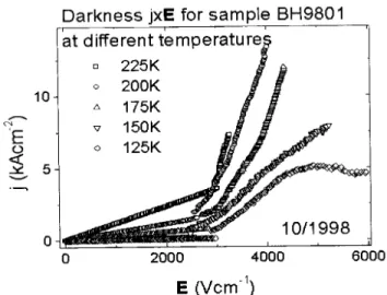
The temperature dependence of thejxE
character-istic in darkness is show in Figs. 1 and 2. The threshold eld is around 3000, 2550, 2850, 2550, and 3000 Vcm,1
at 125, 150, 175, 200, and 225K, respectively. These uctuations in the threshold eld value are related to the change in the free carrier density. The uctuations are controlled by the Fermi distribution of the defect in-volved with the impact ionization process and the com-pensation character of the deep levels, which is a func-tion of its carrier lifetime. We have also observed that the slope ofjxEcurve in the impact ionization regime
reduces for decreasing temperature. For temperatures below about 150K thejxEcurve bends downward even
in the non-linear regime. In this situation even a NNDC behavior could be observed.
For the results shown in Fig. 2 the intensity of the jump in the current density at the breakdown is sig-nicantly stronger than those observed at higher tem-peratures and the value of the threshold eld decreases monotonicallyfor increasing temperatures. The thresh-old elds are 8600 and 5000 Vcm,1 at 25 and 100 K,
respectively. In this temperature range the carrier life-time for the decay into the deep levels of the AsGadefect
is longer than the band to band recombination time. Therefore the impact ionization process depends basi-cally on the free carriers provided by the Fermi distri-bution of carriers from the deep trap involved in the im-pact ionization process. Another characteristic of these measurements is that the current after the threshold shows complex behaviors.
Figure 1. Two eects can be observed in thesejxE
charac-teristics: a) the behavior of the threshold, which uctuates for T in the range 300-125K; b) the form of the current density. For temperatures below 125K see g.2.
Figure 2. The slope of thejxEcharacteristics changes
dras-tically after the threshold and it decreases with the tem-perature as can be seen in the inset. The current density after the threshold shows complex behavior presenting low frequency oscillations, NNDC region and many changes in the slope.
II.2 Sample BH9525
The temperature dependence of thejxE
character-istic in darkness is show in Fig. 3. For temperatures bellow 225K the threshold was not observed at least for electric elds up to around 6000Vcm,1. Otherwise,
Brazilian Journal of Physics, vol. 29, no. 4, Dezembro, 1999 795 measurements at 296K a second threshold could be
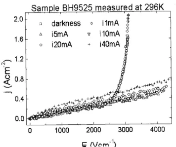
ob-served around 3000Vcm,1. Fig. 4 shows the
jxE
char-acteristics at 296K as a function of the illumination in-tensity. The value of the threshold eld increases with the light intensity. In the range from 200K to 300K the slope of the curves after the threshold does not change with illumination but the jump intensity in the current density does. Under illumination the current density shows an ohmic regime only for very low electric elds and it changes to a sublinear regime that is preserved up to the threshold.
Figure 3. Until 6000Vcm,1, no threshold could be observed
bellow 225K in thejxEcurve. At 296K a second threshold
can be observed around 3000Vcm,1.
Figure 4. The threshold and the jump in the current den-sity increase with the light intenden-sity but the curve ts each other after the threshold.
In Fig. 5 we show the jxE characteristics under
illumination at 225K. The value of the threshold eld increases with the light intensity in the same way as ob-served at 296K. Two thresholds could be obob-served. The
slope after the rst threshold is smaller than that after the second one, which suggests impact ionization in two dierent defects. The slope after the second seems to be same as observed at 296K. The sublinear behavior occurs for electric elds higher than about 500Vcm,1
and we claim that it is associated with eld enhanced trapping. This assumption is corroborated by the pres-ence of LFO.
Figure 5. At 225K and below two thresholds were observed. The rst has a smaller slope than the second. The slope of the current density after the second threshold seems to be related with the same phenomena as that observed at 296K. Above 500Vcm,1, a sublinear behavior is observed which is
probably related to eld enhanced trapping.
III Discussion
We have observed impurity breakdowns, which switches between the low and high current density for both sam-ples, with a threshold eld around 2500 Vcm,1 at
225K. This threshold is too low to be related with the threshold switching of an EL2-like center (which is ex-pected to occurs at around 8kVcm,1). Because of the
LT growth our samples should present a high density of such defects. Therefore the threshold we are observ-ing may be related to other traps. The increase in the value of the threshold eld with illumination for sam-ple BH9525 suggests that impact ionization generates a dierent type of carrier rather than the one who deter-mines the transport mechanism at low elds. Indeed we know that the EL2-like or AsGadeep levels releases
car-riers preferably in the conduction band for the infrared light we are using. In darkness we found a Hall mobil-ity and a Hall p-type carrier densmobil-ity of 560cm2/V.s and
796 R.M.Rubingeret al.
In contrast, for sample BH9801 we have observed a decrease in the threshold eld with illumination in-tensity. This suggests an enhancement in the carrier density under illumination involved in the impact ion-ization. For this sample the presence of strong LFO disturbs the Hall measurements and it was not possi-ble to obtain reliapossi-ble values for the mobility and carrier density.
Using the same procedure of other authors [2] we have assessed the energy associated with the impact ionization. For sample BH9525 we found m=560cm2/V.s; l=2x10,6cm; e=41meV. l is the mean
free path and e is the transition energy. These values are more compatible with holes then with electrons. At this point one might ask if 300K is not a too high tem-perature for the existence of not ionized acceptors in a density high enough in order to induce impact ion-ization. We have calculated the Fermi distribution of holes due to this level and found 21% at 300K; 9.5% at 200K; 0.9% at 100K; and 10,19% at 10K.
Comparing the results with those of a GaAs:Cr sam-ple, having a mobility of 4000cm2/V.s, p~1x107cm,3,
and a mean free path of l=5.5x10,6cm, we found
e=87meV. Such an energy of 87meV is responsible for the release, through impact ionization, of electrons in the conduction band. Otherwise the eect of light is to
release holes in the valence band. Thus, we claim that the same mechanism is responsible for the increase in the threshold eld observed for sample BH9525.
In summary, we have measured the impurity break-down of two LT-MBE GaAs samples at variable tem-perature and illumination conditions. Sample BH9801 shows a breakdown of the same type of the main free carriers and below 100K shows a clear dependence of the threshold on the temperature. Sample BH9525, shows a breakdown of an acceptor level at 41meV from the valence band which increases the threshold under illumination due to the generation of free electrons by the EL2-like deep levels. This behavior is also observed for a GaAs:Cr sample.
References
[1] J. Hirschinger, F. -F. Niedernostheide, W. Prettl, V. Novak, and H. Kostial, Phys. Stat. Sol. 204, 477
(1997).
[2] C. Paracchini and V. Dallacasa, Solid State Comm.69,
49 (1989).
[3] K. Krambrock, M. Linde, J. M. Spaeth, D.C. Look, D. Bliss, and W. Walukiewicz, Semicond. Sci. Technol.7,