*e-mail: [email protected]
Glass Difractive Optical Elements (DOEs)
with Complex Modulation DLC Thin Film Coated
Marina Sparvoli*, Ronaldo Domingues Mansano
Laboratório de Sistemas Integráveis, Departamento de Engenharia de Sistemas Eletrônicos,
Escola Politécnica da Universidade de São Paulo – USP,
Av. Prof. Luciano Gualberto, trav. 3, 153, 05508-900 São Paulo - SP, Brazil
Received: December 15, 2007; Revised: August 5, 2008
We developed a complex (amplitude and phase) modulation Diffractive Optical Element (DOE) with four phase levels, which is based in a glass substrate coated with DLC (Diamond Like Carbon) thin film as the amplitude modulator. The DLC film was deposited by magnetron reactive sputtering with a graphite target and methane gas in an optical glass surface. The glass and DLC film roughness were measured using non destructive methods, such as a high step meter, Atomic Force Microscopy and Diffuse Reflectance. Other properties, such as refractive index of both materials were measured. The DOEs were tested using 632.8 nm HeNe laser.
Keywords: diamond like carbon, glass, diffractive optical elements
1. Introduction
Diffractive optical elements (DOEs) are wavefront processors used to change the distribution of an incident light beam with known properties into a specified pattern1. There are two main types of DOE:
one is amplitude based and the other is contrast. The phase-contrast is more efficient than the amplitude DOEs2. The objective
of this study was the development of diffractive optical elements (DOE’s), fabricated on B 270 glass substrate, with four phase-modulation and amplitude phase-modulation. The amplitude phase-modulation is produced by DLC thin films (Diamond Like Carbon) deposited over glass. A DOE is a component that works according to Huygens principle3-7 and modifies wavefronts by segmenting and redirecting
the segments through the use of interference and phase control. Compared with refractive elements, DOE’s are lighter, occupy a relatively lesser volume and they can be fabricated using micro-electronic processes. Thus they can be built in large scale with high reproducibility, and eliminating almost all the stages traditionally used in optic elements fabrication, as abrasion and burnishing8.
Furthermore, the advantages include:
• Theirfunctionallexibility;wherebyanelementcanperform one or more complex functions simultaneously e.g. beam split-ting and focusing;
• Ease of replication makes production fast, affordable and relatively simple; and
• Parallel performance of similar or different functions such as the multifocus hololens array for parallel pattern recogni-tion.
In this work it is presented the development of diffractive optic devices based in optical glass B 270 from Schott, which present low fabrication cost and have a large transmittance range from 300 to 1,000 nm, becoming possible their use in visible light range.
These devices can be applied in the prototyping of optic systems that can be used in day-by-day equipments such as sensor of position and presence, artificial vision, etc.9-11
The DLC film of this device works as an amplitude modulator. Diamond like carbon (DLC) is a metastable form of amorphous
carbon containing a significant fraction of sp3 bond. It can have a high mechanical hardness, chemical inertness, optical transparency, and it is a wide band gap semiconductor. DLC films have widespread applications as protective coatings and microeletromechanical devices (MEMs)12. The sp2 - bonded carbons form π − π bonding network
that is responsible for the optical properties like the optical gap and infrared refractive index16.
2. Materials and Methods
2.1. Devices with four phase levels fabrication
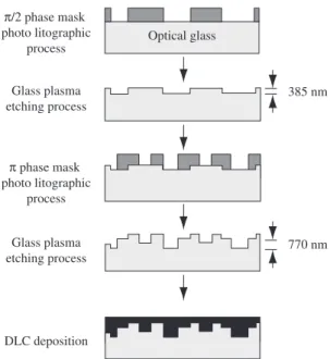
The device fabrication folowed the sequence of Figure 1. For the development of this work, Schott B 270 optical glass substrates with 75 mm diameter and 1 mm thickness with a thermally evaporated thin layer of aluminium were used.
To obtain the two first levels (after the photolitographic process to obtain the π/2 phase, aluminum wet etching and photoresist remotion) plasma etching process was peformed with pure CF4 plasma with 48 sccm gas flow. The etching was made with 100 mTorr pressure, 400 W RF power and under temperature of 5 °C.
With the intention to obtain the final device with four phase levels that will operate with HeNe laser (wavelenght = 632.8 nm), it was made a photo litographic process again for the π phase, aluminum wet etching followed by photo resist remotion and finally, glas etching process with the same parameters of the first etching.
2.2. DLC deposition process
After the second plasma etching and photoresist remotion, the deposition of thin amorphous carbon films was performed by magnetron sputtering system using a graphite pure (99.999%) tar-get with 150 mm diameter. Using a vacuum system composed by a turbo-molecular pump and a root pump, a (residual) pressure of 4.10–6 Torr was obtained. The process pressure 5.10–3 Torr and the
termopar not higher than 90 °C). Along the deposition, the total gas flow in the process was 70 sccm.
2.3. Four levels devices analysis
A system with a 633 nm HeNe laser, three lens, a pin hole, a ccd camera and a bulkhead for the optical analysis was built (Figure 2).
3. Results and Discussion
Before DOE fabrication, the etch rate and roughness of optical glass to obtain the etch process control were studied. Silicon Dioxide (SiO2) can easily be etched by CF4, but the optical glasses show dif-ficulty for these processes because of the high contamination level. In etch process was used a CF4 pure plasma and 5 °C electrode temperature. Pressure was kept constant in 100 mTorr and power level was varied in order to obtain a process which has a reasonable carbon etch rate and minimized roughness.
Before the etch process, elipsometer and high step meter analyses were performed. The optical glass B 270 refraction index measured was 1.41. Etch rate was measured by high step meter for the different samples, as showed in the following graphic. Roughness was obtained by mechanical technique high step meter.
Higher etching process powers were used because those etch rates in brand glass for low power were very insignificant. In fact, it was showed in the graphic (Figure 3) that the higher the RF power is, higher the etch rate will be. Those results can be confirmed when
compared with the results showed in many other articles12-15. The
values for maximum roughness, RMS roughness and RA roughness were between 9.9-40 nm, 0.7-5.4 nm and 1.7-15.8 nm, respectively. So, it proves that the roughness do not vary too much with increas-ing RF power. Consequently, the process with higher RF power was chosen.
The values in pressure of 100 mTorr and an RF power level of 400 W for maximum roughness, RMS roughness and RA roughness, showed around 40 nm, 5.4 nm and 6.7 nm respectively. RMS rough-ness should be smaller than 10% of the wavelength of HeNe laser for the best performance of the diffractive optical element.
The RMS roughness was measured with an AFM. These results could be compared with the results obtained by high step meter.
The result for RMS roghness was low (Figure 4), under the 63 nm limit value (1/10 of HeNe laser wavelenght), but this value is two times bigger than the obtained by high step meter (5.4 nm). Before the glass superficial roughness analysis, it was deposited the DLC (refraction index 1.66) by sputtering with 484 thickness and 3.16 RMS roughness (obtained by high step meter).
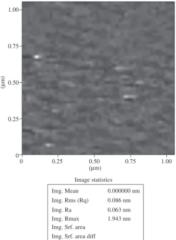
The DLC roughness was measured with AFM technique. The result showed for RMS roughness in AFM measurement (Figure 5) was very low (0.086 nm).
In order to analyse the diffractive optical elements working, it was chosen two Fresnel devices: one that forms an eagle and another that forms a butterfly image (Figure 6).
In Figure 6 are presented typical reconstructions from binary phase diffractive optical elements, Fresnel type. It can observe that there is no presence of diffraction zero order spot on the images that were rebuilt with good fidelity, but with excessive noise speckle (due to the glass etching process that is problematic).
In holograms of Fresnel type the reconstruction is not due to be symmetrically in relation to the reconstruction plan center. It was
Optical glass
π/2 phase mask photo litographic
process
π phase mask photo litographic
process Glass plasma etching process
Glass plasma etching process
DLC deposition
385 nm
770 nm
Figure 1. DOEs with four phase levels and amplitude modulation
fabrica-tion sequence.
Lens
Lens
Lens
Pin hole Obturator Reconstruction
Plan DOE
1200 mm
50 mm d
Laser CCD
250 mm
Figure 2. Optical analyses. The d distance controls the image magnificence.
0 50 100 150 200 250 300 350 400 450
0 20 40 60 80 100 120 140 160 180
Glass etch rate (nm/minute)
Power (W) 100 mTorr pressure
observed that there were no significant differences in the amplitude modulation for the devices covered by DLC and the elements without such thin film. To investigate this, an optical analysis was made of the surface elements. Transmittance results are shown in Figure 7.
The transmitance graphics showed for devices with DLC and without this thin film just prove that the same behavior occurs and the images produced by devices are in fact similar.
It would be ideal devices for to produce lasers with low lenghts (for example in blue range – Ar laser that has 481 nm wave-lenght or in UV range – nitrogen laser that has 337 wavewave-lenght). Another alternative to modulate the amplitude and, using HeNe laser, would be the deposition of a thick DLC layer.
In Table 1 is shown the amplitude modulation eficience from the transmitance difference (T%) for the surface with and without
Image statistics
Img. Ra Img. Mean
Img. Rms (Rq)
Img. Rmax
0.007 nm
10.279 nm
7.962 nm 603.301 nm Img. Srf. area
Img. Srf. area diff
0 1.00 2.00
( m)
(
m)
Figure 4. AFM analyses of 100 mTorr and 400 W sample.
Image statistics
Img. Ra Img. Mean Img. Rms (Rq)
Img. Rmax
0.000000 nm 0.086 nm
0.063 nm 1.943 nm Img. Srf. area
Img. Srf. area diff m
(
m)
Figure 5. AFM analyses of DLC surface.
Figure 6. Device images that reproduce a butterfly and an eagle.
400 600 800 1000
0 20 40 60 80 100
T
ransmittance (%)
Wavelenght (nm) 632.8 nm
(a) Virgin glass (b) Etched glass
(c) DLC over virgin glass (d) DLC over etched glass 200
(a)
(d) (c)
(b)
Figure 7. Virgin glass, etched glass and DLC over glass transmittance.
Table 1. Comparation of calculated results for different lasers.
Laser (nm)
Difference T%
Limit roughness
(nm)
Time (minutes)
Dmax (nm)
HeNe (632,8) ~1 ~63 6.5 770
Argon (481) 5 ~48 5 587
Cumarina (450) 7.5 ~45 4.6 549
DLC thin film in differents wavelenghts, as well the limit RMS roughness, etching process time (for same parameters used in this work: 100 mTorr pressure and 400 W RF power) and the desired thickness.
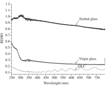
In order to make a more complete study, the total and diffuse reflectances were obtained by spectrophotometry technique with a integrative sphere for all materials. Based on the results, it was possible to calculate the RMS roughness. Using this method we can obtain the real roughness showed by the sample to the incident laser beam interaction.
The materials reflectance analyses is shown in Figure 8. For the plasma etched glass (under 100 mTorr pressure and 400 W RF power, the same parameters used for diffractive devices manufacture), the difference between the values of the total reflectance R0 and diffuse reflectance RD was lower than 1.4% (at a 632.8 nm wavelength), while for the virgin glass, this difference exceeded 7.8%. These val-ues are reflected in the curves RD/R0 (Figure 8) for virgin glass and etched glass. Consequently, the observed roughness for etched glass is greater. In this work, what really matters are the obtained results for 632.8 nm HeNe laser wavelenght.
The measured roughness for DLC was 18.8 nm for HeNe wave-lenght or, in other words, a close value of virgin glass. It indicates that the use of glass as substrate puts a limit in DLC RMS roughness, avoid a lower value. It can be concluded that the substrate would be a limiting factor in DOEs fabrication with DLC thin films.
The Equation for RMS roughness calculation is shown.
2 4 0 RD R π∆
= λ (1)
The values obtained for roughness by Equation 117-22 indicates
that both the glasses that suffered etching process and the DLC coated glasses have a high level of roughness. However these roughness are still within the limit of 63 nm, thus not interfering with the perform-ance of diffractive optical elements manufactured.
In fact, the etched glass presents a RMS roughness greater value (∆) and this can be explained by the fact that the bombardment of the surface by ions during etching increases the roughness, affecting the substrate reflectance (Table 2).
It was also done a RMS roughness study of the DLC obtained by spectrophotometry for different types of lasers (Table 3).
We can observe that roughness decrease for lower wavelenghts. In fact, It’s more beneficial to DOEs fabrication for lasers that oper-ate in UV range.
4. Conclusions
In this work, DOEs based in glass substrate coated with DLC thin film with complex modulation (amplitude and phase) were obtained.
The transmitance graphics showed for devices with DLC and without this thin film just prove that they present the same behavior and the images produced by devices are in fact similar. There is a little difference in used laser wavelenght values (around 1%).
The showed results confirm the possibility to manufactured DOEs to work in the UV region using the DLC as material for the amplitude modulation. The RMS roughness values for the DLC (for different wavelengths) were obtained optically very low, which is good for the device operation.
Besides, the DLC is a material that is compatible with many other substrates as quartz and polymers, and opens a big possibility for production of many DOEs types more eficients and with low cost.
Acknowledgements
The authors would like to thanks to Dr. José Fernando Diniz Chubaci, Mikiya Muramatsu, Dr. Sebastião Gomes do Santos, Dr. Luís da Silva Zambom, Mr. Alexandre Marques Camponucci and Mr.NelsonOrdonezfortechnicalsupportandFAPESP,CNPqand CAPESforinancialsupport.
References
1. Toma SN, Alexandrescu A, Cristea D, Muller R, Kusko M, Dumbravescu N, Nascov V, Cojoc D. Binary phase reflective diffractive optical elements design and fabrication. IEEE. 2004; 2:401-404.
2. KuskoM,CojocD,ApostolD,MullerR,ManeaE,PodaruC.Designand fabrication of Diffractive Optical Elements. IEEE. 2003; 1:167-170. 3. Rotich S, Smith JG, EvansAGR, BrunnschweilerAJ. Photoresist
parabolas for curved micromirrors. Micromechanical Engineering. 1998; 8(2):108-110.
4. Li Q, Gao H, Dong Y, Shen Z, Wang Q. Investigation of diffractive optical element for shaping a gaussian beam into a ring shaped pattern. Optics
& Laser Technology. 1998; 30(8):511-514.
5. Silvennoinen R. et al. Diffractive element in optical inspection of paper.
Optical Engineering. 1998; 37:1482-1487.
250 300 350 400 450 500 550 600 650 700 750 0.1 0.2 0.3 0.4 0.5 0.6 0.7 0.8 0.9 1.0 1.1 1.2 Virgin glass RD/R0 Wavelenght (nm) Etched glass DLC
Figure 8. RD/R0 vs. wavelenght for different materials.
Table 3. DLC RMS roughness obtained with optical technique for different
wavelenghts.
λ (nm) RD/R0 Roughness (nm)
632.8 0.14 18.8
481 0.11 12.7
450 0.10 11.3
337 0.11 8.9
Table 2. Reflectances and RMS roughness results obtained by optical
method.
To λ = 632.8 nm Virgin glass Etched glass DLC
R0-RD 7.8% 1.4% 10.42%
RD/R0 0.24 0.86 0.14
6. Remillard JT, Marinelli MA, Fohl T, O’Neil DA. Diode laser illuminated automotive brake lamp using a linear fan-out diffractive optical element.
Technical Digest of Diffractive Optics and Micro-Optics (DOMO). 1998;
10:192-194.
7. VolkelR,HerzigHP,NussbaumP,DandlikerR,HugleWB.Microlens array imaging system for photolithography. Optical Engineering, 1996; 35(11):3323-3330.
8. Cirino GA. Fabricaçãode elementos ópticos difrativos empregando
processos de microusinagem. [Tese de Doutorado]. São Paulo:
UniversidadedeSãoPaulo;2002.
9. Turunen J, Wyrowski F. Diffractive Optics for Industrial and Commercial
Applications. Berlin: Akademie Verlag; 1997.
10. Goodman JW. Engineering Optics. New York: McGraw Hill; 1996.
11. Veldkamp WB. Wireless focal planes: on the road to amacronic sensors. IEEE. J. Quantum Electronics. 1993; 29(2):801-813.
12. Robertson J. Diamond-like amorphous carbon. Material Science and
Engineering. 2002; 37:129-281.
13. Fieldsien J, Kim D, Economou DJ. SiO2 etching in inductively coupled C2F6 plasmas: surface chemistry and two-dimensional simulations. Thin
Solid Films. 2000; 374(2):311-325.
14. ParkJH,LeeNE,LeeJ,ParkJS,ParkHD.Deepdryetchingofborosilicate glass using SF6 and SF6/Ar inductively coupled plasmas. Microelectronic
Engineering. 2005; 82(2):119-128.
15. LiX,AbeT,EsashiM.DeepreactiveionetchingofPyrexglassusing SF6 plasma. Sensor and ActuatorsA. 2001; 87(3):139-145.
16. Wusirika RA. Study of the relation between the optical gap of diamond-like carbon and deposition conditions and the growth of diamond-diamond-like
carbon on metallic substrates. [Tese de Mestrado]. Local de publicação:
Case Western Reserve University; 1999.
17. Bennett JM, Dancy J H. Stylus profiling instrument for measuring statistical properties of smooth optical surfaces. Applied Optics. 1981; 20(10):1785-1802.
18. Duparre A, Ferre-Borrull J, Gliech S, Notni G, Steinert J, Bennett JM. Surface Characterization Techniques for Determining the Root-Mean-SquareRoughnessandPowerSpectralDensitiesofOpticalComponents.
Applied Optics. 2002; 41(1):154-171.
19. GuentherKH,WiererPG,BennettJM.Surfaceroughnessmeasurements of low-scatter mirrors and roughness standards. Applied Optics. 1984; 23:3820-3836.
20. Elson JM, Rahn JP, Bennett JM. Relationship of the total integrated scattering from multilayer-coated optics to angle of incidence, polarization, correlation length, and roughness cross-correlation properties. Applied
Optics. 1983; 22:3207-3219.
21. Bennett JM. Recent developments in surface roughness characterization.
Meas. Sci. Technol.1992; 3(12):1119-1127.