*e-mail: [email protected]
1. Introduction
Due to very limited mutual solubility between Cu and Cr at room temperature, Cu-Cr alloys have been developed to meet increasing industrial requirements for its outstanding combination of high mechanical strength and good electrical conductivities1-5. Because of high withstand voltage and exceptional current breaking capacity, Cu-Cr alloys have been considered as the best contact material for medium voltage vacuum interrupter4. Wang et al.2 reported that the grain size and distribution of Cr phases was critical to reduce chopping currents and sustain high voltage breakdown strength capacity. The iner the Cr-rich phase was, the better the electric contact materials properties could be achieved. In order to further improve electrical and mechanical properties, many efforts have been focused on reining and homogenizing the Cr-rich phase. Rapid solidiication is believed to be able to reine microstructure and induce supersaturated solid solution, and thus was used by many researchers to prepare Cu-Cr alloys. To date, various methods of rapid solidiication have been successfully explored, such as melt spinning4,5, splat quenching6, gas atomizing and electromagnetic levitation7. In these work, ine Cr-rich spheroids were detected in Cu matrix and attributed to occurrence of the liquid phase separation during rapid solidiication.
As a promising high-energy beam surface modiication technique, high current pulsed electron beam (HCPEB) has been developed in recent years8. Because of good thermal conductivity of metal substrates, main features of HCPEB include rapid heating, melting, vaporization and cooling.
Besides, stress waves, shock waves, vibration and other physical phenomena can also be induced on the material surface, which results in extraordinary modiication effects, such as improved strength, microhardness, wear resistance and corrosion resistant properties9-11. Therefore, by using HCPEB surface modiication techniques, many researchers had studied the surface strengthening and surface alloying of steels, magnesium alloys, aluminium alloys, etc11.
The failure of vacuum interrupter usually occurs on the surface of Cu-Cr contact materials during usage. However, there are few efforts concentrated on the surface modiication of the Cu-Cr alloys. As far as the studies of HCPEB concerned, only Lamperti et al.12,13 reported the surface microstructure of HCPEB-treated Cu-30Cr alloy by use of secondary ion mass spectrometry and atomic force microscopy. However, mechanism of the craters and cracks has not been analyzed. In the current investigation, the microstructure and crater evolution under HCPEB treatment on the surface modiication in CuCr25 and CuCr50 alloys were studied with different pulse numbers.
2. Experimental
The CuCr25 (75wt.%Cu and 25wt.%Cr) master material was prepared by vacuum induction melting ( VIM ) while the CuCr50 master (50wt.%Cu and 50wt.%Cr) material was prepared by iniltrating. After polishing, the CuCr50 alloy was deposited with a Cr ilm using FJL560A ultrahigh vacuum magnetron sputtering equipment. An “RITM-2M” type HCPEB machine was applied with pulse numbers of
Microstructure and Liquid Phase Separation of CuCr Alloys Treated by
High Current Pulsed Electron Beam
Zhiming Zhoua, Tao Zhoua, Linjiang Chaia*, Jian Tua, Yaping Wangb,
Weijiu Huanga, Hongmei Xiaoa, Zhipei Xiaoa
aSchool of Materials Science and Engineering, Chongqing University of Technology,
Chongqing, 400054, China
bSchool of Science, Xi’an Jiaotong University, Xi’an, 710049, China
Received: September 8, 2014; Revised: April 12, 2015
Microstructures of CuCr25 and CuCr50 alloys treated by high current pulsed electron beam (HCPEB) were investigated in this work. The microstructure and solidiication behavior of the Cr-rich phases were characterized by scanning electron microscopy (SEM). Results show that a remelting layer of 3~5 μm is formed on the surface of Cu-Cr alloys. The microstructure of the remelting layer reveals that both the ine dispersion of Cr-rich spheroids and the craters appear after HCPEB treatment. This means that metastable liquid phase separation occurs during rapid solidiication under HCPEB treatment. In addition, the appearance of relatively large craters in the subsurface of Cr-rich particles with the distance about 5-10 μm provides direct evidences supporting results reported by other researchers in terms of numerical simulation temperature ield of HCPEB treatments.
30 and 50. The HCPEB treatment was performed under the following conditions: the electron energy 30 keV, the frequency 0.1 Hz, pulse duration 2 μs, and the vacuum 6×10⁻⁴ Pa. The microstructure and surface morphology after HCPEB treatment were analyzed by JEOL JSM-6460LV scanning electron microscope (SEM). The microstructure of cross-section was etched by FeCl3 (5g) HCl (10 mL) + H2O (90 mL) solution.
3. Experimental Results
Figure 1a illustrates the initial microstructure of CuCr25 alloy prepared by vacuum induction melting. As shown in the igure, the matrix is Cu and the undergrown dendrites are
Cr phases. Figure 1b illustrates the microstructure of the master CuCr50 alloy prepared by iniltrating. It comprises coarse Cr particles distributed in the Cu matrix.
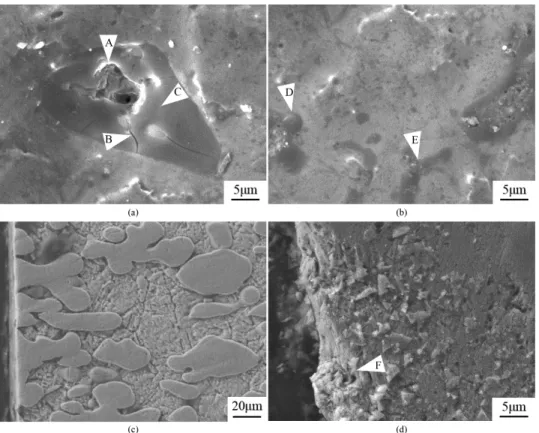
Surface morphologies of the CuCr25 alloy after HCPEB treatment is shown in Figure 2a and Figure 2b. The microstructure of the remelting layer is signiicantly different from that of the master alloy (Figure 1). The coarse Cr-rich dendrites cannot be seen. Various microstructure features are observed in Figure 2a: the large craters as denoted by the arrow A; the cracks near the crater as indicated by the arrow B; the splashed layer as indicated by the arrow C. Figure 2b indicates that the large Cr-rich spheroids (marked
Figure 1. Micrographs showing the microstructures of Cu-Cr master alloy (gray=Cr-rich, light=Cu-rich) (a) CuCr25 alloy; (b) CuCr50 alloy.
by arrow D) and irregular Cr-rich lows (marked by arrow E) occurr. A large number of Cr-rich spheroids with different diameters distribute on the surface. The dimension of Cr-rich spheroids varies from about 100 nm to more than 2 μm. Figure 2c and Figure 2d show the cross-section microstructures of the HCPEB-treated CuCr25 alloy. As can be seen from Figure 2c, a remelting layer with about 3-5 μm in thickness exists. The depth of the craters is about 10 μm (denoted by the arrow F in Figure 2d).
Figure 3 illustrates the microstructure of the CuCr50 alloys after HCPEB treatment. As shown in Figure 3a, after 50-pulse HCPEB treatment, the number of cracks in Cr particles increases, and Cr phase in the Cu-rich matrix is further reined, and the interface of the Cr-rich particles and the Cu-rich phase becomes unclear. Meanwhile, a lot of small Cr-rich spheres appear in the Cu-rich matrix. The cross-section microstructures of alloys are shown in Figure 3b and Figure 3c. After the HCPEB treatment, the thickness of remelting layer in CuCr50 alloys increases to about 3~5 μm. As revealed by the arrows A in Figure 3b and B in Figure 3c, larger craters than cracks in CuCr50 alloy are about 5~10μm in the distance from the surface.
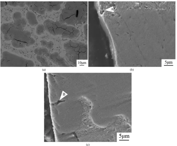
The microstructure of the CuCr50 alloys coated with Cr ilms after 50-pulse HCPEB treatment is shown in Figure 4. The cross-section microstructure of the magnetron sputtered
Cr ilm can be seen in Figure 4a. It can be found that Cr layer with a thickness of 2μm is uniformly coated on the alloy surface (marked by arrow A). The surface microstructure of the CuCr50 coated with Cr after 50-pulse HCPEB treatment is shown in Figure 4b. Many cracks appear in Cr particles and the Cr phases are reined. The interfaces between the Cr particles and the Cu matrix become unclear. As indicated by arrow B, a lot of small Cr-rich spheroids exist in the Cu-rich matrix. The cross-section microstructures of CuCr50 alloys after HCPEB treatment are shown in Figure 4c and Figure 4d. The remelting layer with 3~5 μm in thickness occur in HCPEB-treated CuCr50 alloy (marked by arrow C in Figure 4c). As revealed by the arrow D in Figure 4d, the larger craters than cracks in the Cr particles are about 5~10 μm in the distance from the surface.
4. Discussion
Similar to the Cu-Co14 and Cu-Fe15 systems, the Cu-Cr system is a liquid metastable binary system with a large positive heat of mixing. Müller16 suggested that the Cu-Cr system falls into a monotectic type with a stable miscibility gap. Recently, Zhou et al.8 proposed a novel monotectic type Cu-Cr phase diagram, which displays a stable miscibility gap over compositions between 50.8 and 83.2 wt.% Cr at a
monotectic temperature of 2020 K, where there were liquid spinodal lines and dash lines indicated the MG (binodal lines), respectively. When the Cu-Cr melt was cooled below a certain temperature, the liquid would enter the MG zone and be separated into Cu-rich liquid and Cr-rich liquid, thus leading to the liquid phase separation8. Our previous studies experimentally conirmed that the liquid phase separation will occur in the rapidly solidiication Cu-Cr alloys by melt spinning, splat quenching and electromagnetic levitation4,6,7.
The electron beam will disappear suddenly at the end of every pulse, suggesting a extremely short duration. It means that the melt will cool down and solidify rapidly due to the excellent heat conduction ability of the matrix of Cu-Cr alloy. Because of the heat generated by HCPEB bombardment, substantial thermal stress will be produced, thus making it possible to induce cracks in Cr particles17 (as shown in Figure 2a, Figure 3a and Figure 4b). When the electron beams irradiate the original chapped Cr phases again, coarse craters or cavities will occur in Cu-Cr alloys (marked by arrows A in Figure 2a and F in Figure 2d, A and B in Figure 3, and D in Figure 4d). Moreover, as shown in Figure 2a, splashing phenomenon and cracks are found in the crater. The craters are the consequence of the eruption of melted metal pools18. In addition, as shown in Figure 3a and Figure 4b, since the heat of HCPEB can make the alloy surface remelt and solidify repeatedly, the interface between
Cr-rich particles and Cu-rich matrix become fuzzy. In this study, as shown in Figures 2c, 3b and 4c, the remelting layer with about 3-5 μm in thickness is formed in Cu-Cr alloys due to the ultra high cooling rate and the extremely large supercooling degree during HCPEB treatment. As a result, all the Cu-Cr melts in the composition range enter the MG zone. Therefore, the Cu-Cr alloy will not be heated uniformly by the electron beam, which will cause a low of the melt and the grown Cr-rich droplets will be elongated and swirled (marked arrow D and E in Figure 2b). Another reason for the formation of the Cu-Cr remelting layer is splashing. Therefore, Cr-rich sheets (marked by the arrow C in Figure 2a) also occur in the craters due to the spraying of the molten pool, the high cooling rate and limited melt low. The cooling rate of the alloy droplets is lower than that of the melts in the pool, and the liquid phase separation and the liquid low proceed simultaneously. In accordance with previously reported results2,19, small Cr-rich droplets form in Cu-Cr remelting layer continuously and some extremely ine Cr-rich particles always appear during the liquid phase separation process.
Figure 5 shows a schematic illustration of the HCPEB-treated Cu-Cr alloy in this experiment. When the switches of HCPEB equipment are turned on, the surface of Cu-Cr alloy is melted and lots of molten pools are formed (as can be seen in Figure 5b). The previous investigation by
Zou et al.17 revealed that the highest temperature appeared in the subsurface of alloys after HCPEB treatment. Due to high temperature remelting of subsurface in Cu-rich matrix and Cr particles, as indicated by arrows A in Figure 3b, B in Figure 3c, and D in Figure 4d, the relatively large craters occurred in the subsurface of Cu-Cr alloy under the action of thermal stress. The depth of the molten pool is about 5-10 μm, which provides direct evidences to the numerical simulation results in Zou et al’s studies17. During the HCPEB treatment, the Cu-Cr alloy will be heated rapidly, and some remolten liquid under the subsurface will be splashed to form the craters, accompanied by the formation of lots of small liquid droplets. When the switches are intermittented, the splashing liquid and droplets will solidify rapidly, then the remelting layer will be formed and the liquid phase separation will occur. The molten pool and liquid phase separation will repeatedly occur. As shown in Figure 5c, the craters and remelting layer occur when the switch is turned off. This reinement of Cr particles can remarkably improve the dielectric strength according to previous reports19. The appearance of Cr-rich spheroids is beneicial to the improvement of the dielectric
strength of the Cu-Cr contact materials. Further studies are needed to understand the remelting layer in Cu-Cr alloy.
5. Conclusions
A remelting layer with a thickness of 3~5 μm forms on the surface of Cu-Cr alloys because of repeated rapid heating and solidifying during the HCPEB treatment. Cr-rich spheroids are observed in the remelting layer, which means that metastable liquid phase separation is involved in the microstructure evolution of rapid solidiication in HCPEB-treated Cu-Cr alloy. The relatively large craters appeared in the subsurface of the specimens provide direct evidences for the numerical simulation results by other researchers.
Acknowledgements
This study is inancially supported by the National Natural Science Foundation of China under grant Nos. 51101177, 51401040, 51171146 and 51171216, the Natural Science Foundation of Chongqing under grant No. cstc2012jjA245.
Figure 5. Schematic illustration of the process of HCPEB treatment for Cu-Cr alloys (a) master Cu-Cr alloy; (b) the splashing and craters during HCPEB treatment; (c) the micrographs after the HCPEB treatment.
References
1. Slade PG. Advances in material development for high power, vacuum interrupter contacts. IEEE Transactions on Components, Packaging and Manufacturing Technology. 1994; 17(1):96-106. 2. Wang YP and Ding BJ. The preparation and the properties of
microcrystalline and nanocrystallineCuCr contact materials. IEEE Transactions on Components, Packaging and Manufacturing Technology. 1999; 22(3):467-472.
3 Zhang C, Wang Y, Yang Z, Guo Y and Bingjun D. Microstructure and properties of vacuum induction melted CuCr25 alloys. Journal of Alloys and Compounds. 2004; 366(1-2):289-292. 4. Zhou ZM, Wang YP, Gao J and Kolbe M. Microstructure of
rapidly solidified Cu–25wt.% Cr alloys. Materials Science and Engineering A. 2005; 398(1-2):318-322. http://dx.doi. org/10.1016/j.msea.2005.03.095.
5 Sun Z, Zhang C, Zhu Y, Yang Z, Ding B and Song X. Microstructures of melt-spun Cu100−x–Crx (x=3.4–25) ribbons. Journal of Alloys and Compounds. 2003; 361(1-2):165-168. 6. Zhou ZM, Gao J, Li F, Zhang YK, Wang YP and Kolbe M. On
the metastable miscibility gap in liquid Cu–Cr alloys. Journal of Materials Science. 2009; 44(14):3793-3799. http://dx.doi. org/10.1007/s10853-009-3511-y.
7. Zhou ZM, Gao J, Li F, Wang YP and Kolbe M. Experimental determination and thermodynamic modeling of phase equilibria in the Cu–Cr system. Journal of Materials Science. 2011; 46(21):7039-7045. http://dx.doi.org/10.1007/s10853-011-5672-8. 8. Zou JX, Zhang KM, Grosdidier T, Dong C, Qin Y, Hao SZ, et al.
Orientation-dependent deformation on 316L stainless steel induced by high-current pulsed electron beam irradiation. Materials Science and Engineering A. 2008; 483–484:302-305. http://dx.doi.org/10.1016/j.msea.2006.07.179.
9. Zou J, Grosdidier T, Zhang K and Dong C. Mechanisms of nanostructure and metastable phase formations in the surface melted layers of a HCPEB-treated D2 steel. Acta Materialia. 2006; 54(20):5409-5419. http://dx.doi.org/10.1016/j. actamat.2006.05.053.
10. Qin Y, Dong C, Wang X, Hao S, Wu A, Zou J, et al. Temperature profile and crater formation induced in high-current pulsed electron beam processing. Journal of Vacuum Science & Technology. A, Vacuum, Surfaces, and Films. 2003; 21(6):1934-1938. http:// dx.doi.org/10.1116/1.1619417.
12. Lamperti A, Ossi PM and Rotshtein VP. Surface analytical chemical imaging and morphology of Cu–Cr alloy. Surface and Coatings Technology. 2006; 200(22-23):6373-6377. http:// dx.doi.org/10.1016/j.surfcoat.2005.11.103.
13. Lamperti A and Ossi PM. SIMS direct surface imaging of Cu1− xCrx formation. Applied Surface Science. 2006; 252(6):2288-2296. http://dx.doi.org/10.1016/j.apsusc.2005.04.015.
14. Munitz A and Abbaschian R. Microstructure of Cu-Co alloys solidified at various supercoolings. Metallurgical and Materials Transactions. A, Physical Metallurgy and Materials Science. 1996; 27(12):4049-4059. http://dx.doi.org/10.1007/BF02595654. 15. He J, Zhao JZ and Ratke L. Solidification microstructure and
dynamics of metastable phase transformation in undercooled liquid Cu–Fe alloys. Acta Materialia. 2006; 54(7):1749-1757. http://dx.doi.org/10.1016/j.actamat.2005.12.023.
16. Müller R. Arc-melted CuCr alloys as contact materials for vacuum interrupters. Siemens Forschungs-und Entwicklungsberichte. 1988; 17:105-111.
17. Qin Y, Zou JX, Dong C, Wang XG, Wu A, Liu Y, et al. Temperature–stress fields and related phenomena induced by a high current pulsed electron beam. Nuclear Instruments & Methods in Physics Research. Section B, Beam Interactions with Materials and Atoms. 2004; 225(4):544-554. http://dx.doi. org/10.1016/j.nimb.2004.06.008.
18. Guan QF, Zhang QY, Dong C, Zou G, et al. Effect of structure defects on the surface craters induced by high current pulsed electron beam. Chinese Journal of Materials Research. 2005; 19:496-500.