Ana Paula Pinto Correia
Licenciada em Ciências da Engenharia de Micro e Nanotecnologias
A Second-Order
ADC using sputtered IGZO TFTs
with multilayer dielectric
Dissertação para obtenção do Grau de Mestre em Engenharia de Micro e Nanotecnologias
Júri:
Presidente: Prof. Doutor Rodrigo Ferrão de Paiva Martins Arguente: Prof. Doutor Nuno Filipe Silva Veríssimo Paulino Vogal: Prof. Doutor Pedro Miguel Cândido Barquinha
Novembro, 2014
Orientador:
Doutor Pedro Miguel Cândido Barquinha,
Professor Auxiliar, Faculdade de Ciências e Tecnologia,
Universidade Nova de Lisboa
Co-orientador: Doutor João Carlos da Palma Goes,
A Second-
Order ΣΔ ADC using
sputtered IGZO TFTs with multilayer dielectric
Copyright © Ana Paula Pinto Correia, Faculdade de Ciências e Tecnologia, Universidade Nova de Lisboa
i
Acknowledgments
Coming together is a beginning; keeping together is progress; working together is success. Henry Ford
There were hours, days, weeks, consecutive months of work, some frustration and much passion, support and guidance. There were people, many people who, with a smile or just with simple encouragement words, helped me to move forward and successfully complete an important stage of my life.
Yes!, there were many people who, even in a simple way, contributed and collaborated on this project – to all of them, my sincerely thank. However, it would be impossible not make reference of some institutions and persons.
To my advisors, Prof. João Goes and Prof. Pedro Barquinha. Firstly, I must thank for the excellent guidance and availability, making sure that without your support and trust, this multidisciplinary project would not become possible. At the same time, your friendship has been, and certainly will continue be!, a strong impulse to my personal and professional development.
To Materials Science Department, Electrical Engineering Department and, specially, to CENIMAT/I3N, CEMOP and CTS/UNINOVA. All persons who form these institutions, allied to fully equipped laboratories and formidable working conditions, provided a realization of a project with this dimension. A particular and sincerely thank to Prof. Elvira Fortunato and Prof. Rodrigo Martins – your effort has located this institution in a privileged place at the international level.
To Silicon & Software Systems (S3 Group) Portugal. Your support and friendship were essential for my continue personal development and for an excellent professional integration. A special thank to Ing. Arnaldo Guerreiro and Ing. Pedro Faria by all technical support.
To Materials for Electronics, Optoelectronics and Nanotechnologies Group. Your help with different equipment, devices production and data obtaining were crucial. In addition, your friendship improved my integration into the group. A sincerely thank to Ing. Ana Rovisco and Ing. Jorge Martins, for their support in clean room, mainly in an initial period. To Dr. Asal Kiazadeh, Dr. Joana Pinto, Ing. Sónia Pereira and Prof. Luís Pereira for helping me with characterization tools.
To all “nearly” Dr. from Micro and Nanolectronics Group (from CTS): Ing. Somayeh Abdollahvand, Ing. Beatrice Moasa, Ing. Blazej Nowacki, Ing. Edinei Santin, Ing. Hugo Serra, Ing. Ivan Bastos and Ing. João de Melo. Your readiness and willingness to help will always be remembered here by the younger member of this room. I could not fail to make a reference to Ing. Edinei Santim for helping me with transistor models and, a special mention to Ing. João de Melo by all support with modulator and simulation tools.
To all my friends of Micro and Nanotechnologies Engineering and Materials Engineering. Your friendship during this way was extremely important. A honestly thank to Daniel Matos, Gonçalo Rodrigues, Inês Cunha, Miguel Soares, Paul Grey, Pedro Baião, and Vasco Rodrigues: I learned a lot with you! A further reference to Catarina Rodrigues and Emanuel Carlos by the encouragement with transistor models and comparator.
To all my friends from North. The distance is no impediment and this is the proof - even far away, you are always close. Thanks for your support and friendship. A special thanks to Sara Pereira, Tiago Cunha and Andreia Soares - your calls transmitting force and courage in the most difficult moments will never be forgotten. Further reference to Luis Ribeiro - a future Electrical and Computer Engineer!
To Ricardo Ferreira. Your patience, understanding, friendship and love over the years.
To my parents, brother and remaining family. It was with you, it was for you! You always will be my pillar, my inspiration, my life. There is no way to express my gratitude, who I am today is due to you, to your love. I love you!
iii Quem não sente a ânsia de ser mais, não chegará a ser nada.
v
Abstract
This dissertation combines materials science and electronics engineering to implement, for the first time, a 2nd-order ∑∆ ADC using oxide TFTs. The transistors employ a sputtered IGZO
semiconductor and an optimized dielectric layer, based on mixtures of sputtered Ta2O5 and SiO2.
These dielectrics are studied in multilayer configurations, being the best results achieved for 7 layers: IG<10 pA and EB>7.5 MV/cm, while keeping κ>10, yielding a major improvement over Ta2O5
single-layer. After annealing at 200 °C, TFTs with these dielectrics exhibit µSAT≈13 cm2/Vs, On/Off≈107 and
S≈0.2 V/dec. An a-Si:H TFT RPI model is adapted to simulate these devices with good fitting to experimental data. Concerning circuits, the ∑∆ architecture is naturally selected to deal with device mismatch. After design optimization, ADC simulations achieve SNDR≈57 dB, DR≈65 dB and power dissipation, approximately, of 22 mW (VDD=10 V), which are above the current state-of-the-art for
competing thin film technologies, such as organics or even LTPS. Mask layouts are currently under verification to enable successful circuit fabrication in the next months.
This work is a major step towards the design of complex multifunctional electronic systems with oxide TFT technology, being integrated in ongoing EU-funded and FCT-funded research projects at CENIMAT and UNINOVA.
Keywords: a-IGZO TFTs; sputtered high-κ dielectrics; multicomponent and multilayers
vii
Resumo
Esta dissertação combina Ciência dos Materiais e Engenharia Eletrotécnica para implementar, pela primeira vez, um ∑∆ ADC de 2ª-ordem usando TFTs de óxido. Os transístores empregam IGZO como semicondutor e um dielétrico baseado em misturas de Ta2O5 e SiO2, sendo todos os materiais
depositados por pulverização-catódica. Os dieléctricos são estudados em configurações multicamada, sendo o melhor resultado obtido para 7 camadas: IG<10 pA e EB>7.5 MV/cm, mantendo κ>10. Depois
de recozidos a 200 °C, os TFTs exibem µSAT≈13 cm2/Vs, On/Off≈107 e S≈0.2 V/dec. O modelo a-Si:H
TFT RPI é adaptado para simular estes dispositivos com bom ajuste aos dados experimentais. Relativamente aos circuitos, a arquitectura por modulação ∑∆ é selecionada para lidar com a variação de desempenho e erros de emparelhamento entre transístores. Após optimização do circuito, as simulações do ADC revelaram: SNDR≈57 dB, DR≈65 dB e dissipação de potência ≈22 mW (VDD=10
V), valores melhores que os permitidos por outras tecnologias de filme fino, como orgânicos ou mesmo LTPS. Actualmente, o desenho das máscaras está sob verificações finais para permitir o fabrico do circuito nos próximos meses.
Este trabalho contribui fortemente para projetar sistemas eletrónicos multifuncionais e complexos com TFTs de óxidos, sendo integrado em projetos de investigação em curso financiados pela UE e FCT no CENIMAT e no CTS/ UNINOVA.
Palavras-chave: a-IGZO TFTs; Dielétricos de elevada permitividade depositados por
ix
Contents
1. Motivation, thesis contribution and structure ... 1
1.1 Contributions ... 2
1.2 Thesis Structure ... 2
2. Introduction ... 3
2.1 Thin-Film Transistors ... 3
2.1.1 TFTs structure and operation ... 3
2.1.2 From conceptual patents to oxide TFTs ... 3
2.2 Analog-to-digital converters ... 6
2.2.1 ΣΔ Modulators ... 7
2.2.2 ADCs using TFTs ... 8
3. Materials and techniques ... 9
3.1 Production techniques ... 9
3.1.1 Sputtering ... 9
3.1.2 Patterning ... 10
3.2 Characterization techniques... 10
3.3 Modeling, Simulation and EDA tools ... 10
4. Results and Discussion ... 11
4.1 Amorphous multicomponent high-κ dielectrics based on Ta2O5 and SiO2: thin films and integration in IGZO TFTs ... 11
4.1.1 Single layer structure using Ta2O5 and TSiO ... 11
4.1.2 Multilayer structures based on TSiO and SiO2 ... 18
4.1.3 IGZO TFT Modeling ... 22
4.2 ΣΔ Modulator: circuit and simulation results ... 23
4.2.1 Comparator ... 23
4.2.2 ΣΔ Modulator ... 26
4.3 Circuit Layout ... 29
x
5.1 Conclusions ... 31
5.2 Future Perspectives ... 32
6. References ... 33
Appendix A - ADCs using TFTs ... 37
Appendix B - TFT production by steps ... 39
Appendix C - Deposition conditions for Mo and IGZO ... 41
Appendix D - Characterization techniques ... 43
Appendix E - Electrical Characterization of devices using Ta2O5 and TSiO ... 45
Appendix F - RBS results ... 49
Appendix G - Electrical Characterization of devices using Multilayer structures ... 51
Appendix H - ΣΔ Modulator ... 55
xi
List of Figures
Figure 1.1 - Concepts of transparent displays: smart window (a) [1]. Concepts of flexible
displays: watch (b) [2] and a display developed by HP Lab (c) [3]. ... 1
Figure 2.1 – Ideal output characteristics of a n-type TFT (adapted from [5]). ... 3
Figure 2.2 – Schematic for the carries transport path for amorphous oxide semiconductors, proposed by Nomura et al. (adapted from [15]). ... 4
Figure 2.3 – Inversely proportional relation between band gap and κ for some dielectrics studied [27]. ... 5
Figure 2.4 – Generic block diagram of an ADC. ... 6
Figure 2.5 – Schematic of oversampling ADC (adapted from [45]). ... 7
Figure 3.1 – TFT structure: staggered bottom gate, top-contacts. ... 9
Figure 4.1 –Diffractogram for Ta2O5 (a) and TSiO (b) thin films, annealed at different temperatures until the crystallization is evident. The data obtained is compared with the ICSD database and corresponds to orthorhombic β- Ta2O5 (ICSD: 98-004-8854). ... 12
Figure 4.2 - AFM analysis, showing the amorphous structures of Ta2O5 and TSiO thin films. .. 13
Figure 4.3 - Spectroscopic ellipsometry analysis: comparison between Ta2O5 and TSiO thin films in terms of refractive index (a) and extinction coefficient (b) with SiO2, as reference. ... 13
Figure 4.4 - Measured I-V characteristics for devices with W/L=160/20µm/µm and annealed at 200 ⁰C. Effect of dielectric composition and the usage of substrate bias in devices with approximately the same thickness (a) and of dielectrics thicknesses considering the same material and the usage of substrate bias(b). ... 15
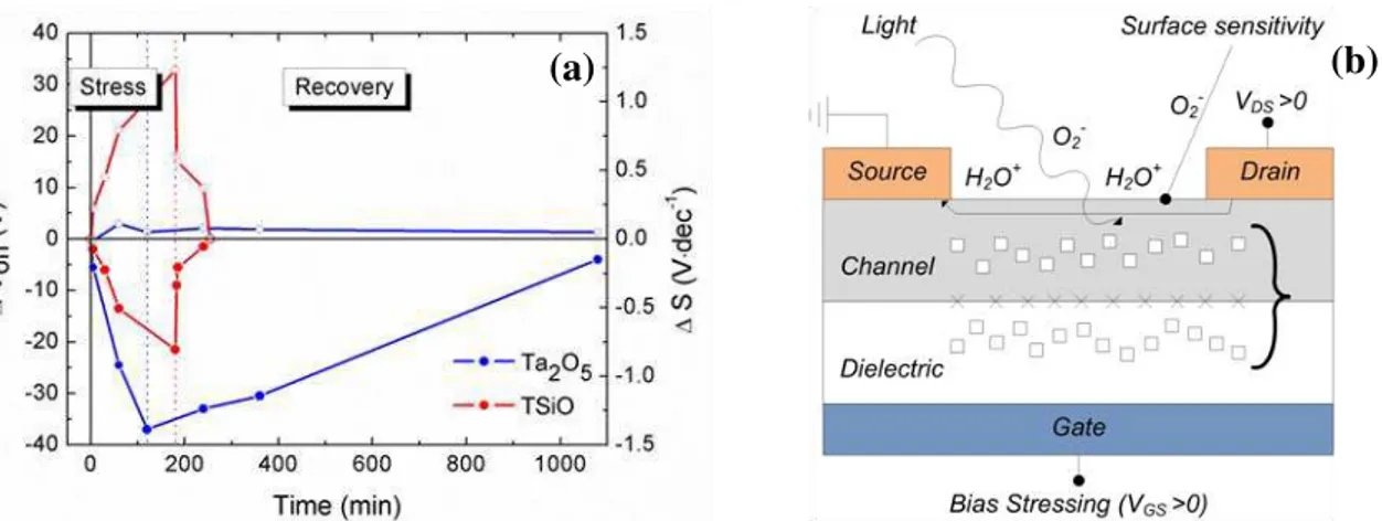
Figure 4.5 – Von and S variations during stress and recovery measurements for TFTs annealed at 200 ⁰C using Ta2O5 and TSiO as dielectric layer for TFTs with W/L = 160/20 µm/µm, applying a gate field of 0.16MV.cm-1in dark (a). Solid and open circles denote ΔV on and ΔS, respectively. Mechanisms involved in AOS and dielectric materials, when a positive gate bias stress is applied in a staggered bottom gate, top contacts structure (b) (adapted from [58]). ... 17
Figure 4.6 – Compositional analysis: comparison between TSiO and multilayers using three and five layers. ... 18
Figure 4.7 - Spectroscopic ellipsometry analysis: comparison between single and multilayers dielectrics thin films in terms of refractive index (a) and extinction coefficient (b) with SiO2, as reference. ... 19
Figure 4.8 - Measured I-V characteristics for devices annealed at different temperature and evaluated in different times, using a medium integration time (a). Effect of integration time in I-V characteristics (b). ... 20
xii Figure 4.10 - Von and S variations during stress and recovery measurements for TFTs annealed
at 200 ⁰C using multilayers structures (W/L = 160/20 µm/µm), applying a gate field of 0.16MV.cm-1.
Solid and open circles denote ΔVon and ΔS, respectively. ... 21
Figure 4.11 - Measured and simulated I-V characteristics for a multilayer device (3 layers) with
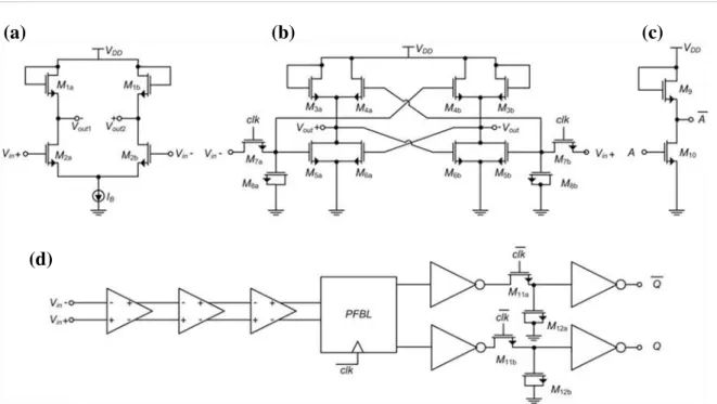
W/L=160/20 µm/µm: transfer curve (a) and output curve (b). ... 22 Figure 4.12 – Schematic of the proposed comparator: pre-amplifier (pre-amp) (a);
positive-feedback latch (PFBL) (b); logic inverter (c) and complete comparator (d). ... 24 Figure 4.13 – Differential output when a input triangular signal is applied (a). Differential
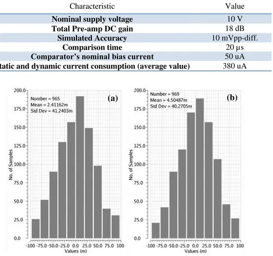
signal with a sequence of eight different comparisons (b). ... 24 Figure 4.14 - Simulated 1-σ random offset voltage (σ(VON) = 50 mV) for VON=0 V @ IB=50 µA
(a) and VON=0.5 V @ IB=30 µA (b). ... 25
Figure 4.15 - Schematic differential 2ndorder CT ΣΔM with feedforward structure: transmission gate D-type fli- flop (a) and the modulator (b).... 27
Figure 4.16 – Simulated FFT assuming a -6dBFS and 100 Hz input signal. ... 28
Figure 4.17 – Obtained output spectrum obtained from electrical simulation of the complete ΣΔ
Modulator (SNDR versus input signal amplitude and SNR versus input signal amplitude). ... 28 Figure 4.18 - Layout of the ΣΔM. ... 30 Figure B.1 - Sequence of steps during a sputtered TFT production. The microscope image was
obtained using Olympus BX51 (100x). ... 39 Figure E.1 - C-f and C-V characteristics of MIM structures that integrated Ta2O5 and TSiO
layers. ... 45 Figure E.2 - Output characteristics of IGZO TFTs with Mo electrodes, using TSiO as dielectric
layer (≈200 nm), annealed at 200 ⁰C. ... 45 Figure E.3 - SEM image of Mo/ dielectric interface, where the “bubbles” effect is visible. ... 46 Figure E.4 - Transfer curves for different devices (from right to left) in the same substrate, using
Ta2O5 (a) and TSiO (b) with a thickness close to 200 nm and annealed at 200 ⁰C. Both dielectrics
were deposited by sputtering with substrate bias. ... 47 Figure E.5 - Transfer curves in double sweep mode using Ta2O5 (a) and TSiO (b) with a
thickness close to 200 nm and annealed at 200 ⁰C. Both dielectrics were deposited by sputtering with
substrate bias ... 47 Figure E.6 - Transfer characteristics evolution for stress and recovery for Ta2O5, (a) and (b),
and for TSiO (c) and (d). ... 48 Figure F.1 - Composition analysis obtained by RBS for IGZO film. ... 49 Figure G.1 - Transfer characteristics evolution for stress and recovery for multilayer (3 layers),
xiii Figure H.1 - Simulation result for inverter considering the load n-type TFT (40/10 µm/µm) and
driver (160/10 µm/µm). ... 55 Figure I.1 - Structure of PCELL used for a 160/10 (µm/µm). ... 57 Figure I.2 - Glass substrate, covered with a Mo thin film, inserted in a PCI connector for
xv
List of Tables
Table 3.1 - Deposition conditions for dielectric layer. All sputtering targets were performed by
SCM.inc. ... 9
Table 4.1 - Properties of Ta2O5 and TSiO films obtained by Tauc-Lorentz dispersion method. . 14 Table 4.2 – Electrical properties of Ta2O5 and TSiO determined from MIM structures. ... 14
Table 4.3 – Summary of electrical properties of devices annealed at 200 ⁰C using different dielectrics in different conditions, depicted in fig. 4.4. ... 16
Table 4.4 - Properties of single and multilayers films obtained by Tauc-Lorentz dispersion method. ... 19
Table 4.5 - Electrical properties of dielectrics determined from MIM structures. ... 20
Table 4.6 – Simulated key performance parameters. ... 25
Table 4.7 –Simulated comparator’s offset with different Von. ... 26
Table 4.8 – Main characteristics of ΣΔM. ... 28
Table A.1 - ADCs using Thin Film Technologies. ... 37
Table C.1 - Deposition conditions for contacts (Mo) and semiconductor layers (IGZO) by sputtering. All sputtering targets were performed by SCM.inc. ... 41
Table D.1 - Main goals and experimental details of characterization techniques used during this work. ... 43
Table F.1 - Parameters obtained for dielectrics after fitting for RBS results. ... 49
Table F.2 - RBS results obtained after fitting of IGZO data. ... 50
Table G.1 - Electrical properties for TFT devices that used multilayers structures (W/L = 160/20 µm/µm). Devices were measured using a short integration time to prevent hump effects (see chapter 4), which increases the measured IG values over more conventional medium integration times. ... 51
Table H.1 - Transistor dimensions used in the initial sizing of the comparator. ... 55
Table H.2 - Transistor dimensions used in the final sizing of the comparator. ... 56
Table H.3 - Sizing of passive elements obtained by SIMULINK®. ... 56
xvii
Symbols
Ci –Gate capacitance per unit area
EB – Breakdown field
EC – Conduction band
Eg – Bandgap
Fs – Sampling frequency
IDS – Drain-to-source current
IG – Gate leakage current
J – Current density k – Extinction coefficient L – Channel length n – Refractive index S – Subthreshold slope VDD – Power supply
VDS – Drain voltage
VGS – Gate voltage
Von - Turn-on voltage
VT – Threshold voltage
W – Channel width κ – Dielectric constant µFE – Field-effect mobility
µsat – Saturation mobility
xix
Acronyms
ADC – Analog-to-digital converter AFM – Atomic force microscopy
AOS – Amorphous oxide semiconductors BW – Bandwidth
CENIMAT – Centro de Investigação de Materiais
CEMOP - Center of Excellence in Microelectronics Optoelectronics and Processes CT – Continuous time
CTS - Centre of Technology and Systems
CMOS – Complementary metal oxide semiconductor DAC – Digital-to-analog converter
DNL – Differential non-linearity DR – Dynamic range
DRC – Design rule check DSP – Digital signal processor DT – Discrete time
EDA – Electronic design automation ENOB – Effective number of bits FFT – Fast Fourier Transform IC – Integrated circuit
IGZO – Gallium indium zinc oxide INL – Integral non-linearity LSB – Least significant bit
LTPS – Low temperature polycrystalline silicon LVS – Layout versus schematic
MESFET – Metal semiconductor field effect transistor MIM – Metal-insulator-metal
MIS – Metal-insulator-semiconductor
MISFET - Metal insulator field effect transistor
MOSFET – Metal oxide semiconductor field effect transistor OSR – Oversampling ratio
PDK – Process-design-kit PFBL – Positive feedback latch
xx SNDR – Signal-to-noise plus distortion ratio
SNR – Signal to noise ratio
TCO – Transparent conducting oxide TFT – Thin-film transistor
TSO – Transparent semiconducting oxide
UNINOVA – Instituto de Desenvolvimento de Novas Tecnologias XRD – X-ray diffraction
∑∆ - Sigma-delta
A Second-Order ΣΔ ADC using sputtered IGZO TFTs with multilayer dielectric
__________________________________________________________________________________
1 Figure 1.1 - Concepts of transparent displays: smart window (a) [1]. Concepts of flexible displays: watch (b) [2]
and a display developed by HP Lab (c) [3].
(a)
(b)
(c)
1.
Motivation, thesis contribution and structure
Transparent electronics is one of the most promising emerging technologies, enabling exciting concepts such as transparent displays. In fact, materials such as transparent semiconducting oxides (TSOs) and transparent conducting oxides (TCOs) allow the mass production of circuits with clear advantages over the ones based on competing thin film technologies, namely in terms of lower processing temperature and costs and excellent performance, typically far superior to a-Si and organics and comparable to LTPS.
In this way, some prototypes of fully transparent displays have been shown, by leading display companies (Samsung, AUO, LG), triggering the concepts of cars and buildings with smart windows or even wearable electronics when oxides are integrated in flexible substrates (fig. 1.1).
The key elements of these displays are transistors and they acquire an important role in the global electronics world since they amplify and switch electronic signals. Thin-film transistors (TFTs) are a particular case of field-effect transistors (FETs) and are of great interest for thin film technologies. Materials used in TFTs naturally determine key device parameters, such as mobility, nominal operating voltage ranges and leakage current. In the particular field of oxide TFTs, indium gallium zinc oxide (IGZO) TFTs have achieved an extreme importance due to the brilliant performance that is obtained at low temperatures (e.g., µFE>10 cm2/Vs with T=150 °C), combined with
excellent large area uniformity. Dielectrics are also crucial defining TFT performance and stability. High dielectric constant (high κ) dielectrics have been integrated in TFTs allowing a thicker film than with SiO2 but maintaining the same capacitance per unit area. This is quite relevant to improve device
performance and reliability, particularly when low processing temperatures are envisaged.
A Second-Order ΣΔ ADC using sputtered IGZO TFTs with multilayer dielectric
__________________________________________________________________________________
2 because despite all real signals are analog it is always desirable to process them, as much as possible, in the digital domain.
Successful design, simulation and fabrication of an ADC is thus a very significant demonstration of the capability of a TFT technology.
1.1
Contributions
Based on this background, the main contributions of this work are:
Optimization of sputtered dielectrics for increased breakdown field and improved IGZO TFT
reliability/performance. This includes the study of single layers (SiO2, Ta2O5 and TSiO) and their
integration in multilayer structures;
Adjust a model based on a-Si:H TFT model developed by Semiconductor Devices Research
Group at RPI, in order to simulate the optimized IGZO TFT behavior;
Design (circuit schematic and mask layout) of a robust second-order sigma-delta (ΣΔ) ADC
based in a power-optimized ΣΔ modulator (ΣΔM), where a special relevance is given to the most critical analog active block – the comparator1.
Produce the circuit prototype and experimentally evaluate it - a future contribution.
1.2
Thesis Structure
The structure of this thesis is as follows:
In Chapter 2 is presented some background related to oxide semiconductors and high-κ
dielectrics used in TFTs. The operation mode of TFTs and a brief state of the art in this area are also reported. Another section comprises operation of ADCs, some architectures and a concise state of the art about ADCs using TFTs;
Chapter 3 summarizes the production technique (sputtering) and materials used during this
thesis work. Characterization techniques and EDA tools are also referred;
Chapter 4 comprises presentation and discussion of the obtained results during the study of
dielectric films and their application to IGZO TFTs. Besides experimental data, device simulation results are also included. The adapted TFT model is then used to simulate the complete designed ΣΔM. Finally, some circuit layout considerations are provided;
The main conclusions and some future perspectives based on the outputs of this work are
included in Chapter 5.
A Second-Order ΣΔ ADC using sputtered IGZO TFTs with multilayer dielectric
__________________________________________________________________________________
3 Figure 2.1 – Ideal output characteristics
of a n-type TFT (adapted from [5]).
2.
Introduction
This chapter summarizes an introductory background and a concise historical perspective related to thin-film transistors (TFTs) and analog-to-digital converters (ADCs) using TFTs. Materials used in the production of TFTs such as transparent semiconducting oxides (TSOs) and high dielectric constant (high-κ) dielectrics will also be briefly explored.
2.1
Thin-Film Transistors
Nowadays, TFTs acquire an important role in electronics world, mainly in active matrix liquid crystal displays (AMLCDs) where they are used to switch each pixel on or off. But TFTs are also used with others goals, for instance, to amplify electronic signals.
2.1.1
TFTs structure and operation
A TFT is a field-effect transistor (FET) comprising three terminals (gate, source and drain), a semiconductor and a dielectric layer. The semiconductor is placed between source/drain contacts, while the dielectric is located between the gate electrode and the semiconductor. The main idea in this device is to control the current between drain and source (IDS) by varying the potential between gate
and source (VGS), inducing free charge accumulation at the dielectric/semiconductor interface [4].
TFTs can be seen as a class of FETs where main emphasis is on large area and low temperature processing, while MOSFETs, where crystalline silicon acts as substrate and semiconductor, are essentially focused in high performance, at the cost of considerably larger processing temperature.
Related with operation mode and considering the n-type TFTs, these can be designated by enhancement or depletion mode depending if threshold voltage
(VT) is positive or negative. When VGS>VT, a significant
density of electrons is accumulated in dielectric/semiconductor interface and a significant IDS starts flowing, depending on
applied drain potential (VDS) – designated by On-state. In this
On-state, there are two regimes depending on value of VDS
(shown in fig. 2.1): if VDS<<VGS-VT the TFT is in linear mode
(IDS increases linearity with VDS) while if VDS>>VGS-VT, the
device is in saturation mode (IDS is independent of VDS) [5].
2.1.2
From conceptual patents to oxide TFTs
A Second-Order ΣΔ ADC using sputtered IGZO TFTs with multilayer dielectric
__________________________________________________________________________________
4 Figure 2.2 – Schematic for the carries transport path for amorphous oxide semiconductors, proposed by Nomura
et al. (adapted from [15]). Brattain and the junction field-effect transistor (JFET) proposed by Shockley in 1952. These were the first transistors that were actually fabricated, showing the switching capability of such devices and how they could be advantageous over the conventional tubes.
In the 60s’, the first TFT was demonstrated and high speed transistors, the MOSFETs, also emerged in this decade. In 1979, the hydrogenated amorphous silicon (a-Si:H) was introduced as a semiconductor on TFTs. Despite its low mobility when compared with the (poly)crystalline materials being studied in that period, the amorphous structure allowed for large area fabrication. Pursuing greater mobility devices, in the 80’s TFTs based on poly-Si were introduced, allowing for high performance circuit fabrication. However, poly-Si TFTs required high temperature processes and had high fabrication cost. Hence, in the 90’s, a low temperature poly-Si (LTPS), around 550 ⁰C, was suggested but the processing in large area is not trivial. Organic TFTs also appeared in this decade and have a fantastic advantage, low processing temperature, although their lack of stability and performance still remains an issue [6]. Hence, there was still space for a new technology, combining large-area uniformity, low processing temperatures and good electrical performance. The answer to this emerged in the new millennium, with the so-called oxide TFTs, which besides these properties also offer the possibility of fully transparent devices.
Transparent conductive oxides (TCOs) and TSOs, whose studies are reported to the beginning of the 20th century, are key materials of transparent electronics, exhibiting optical transparency and
tunable conductivities between those of conductors and semiconductors [5]. The idea behind them is to have intrinsic (structural defects) or extrinsic (substitutional elements) doping during film deposition. For instance, by varying stoichiometry, it is possible to obtain different free carrier concentrations – normally in the 1021 cm-3 range for TCO and from 1014 to 1018 cm-3 for TSO [5, 7, 8].
The first work using a TSO as channel layer in a TFT appeared in the 60’s. A work based on ZnO (zinc oxide) was suggested but with a small IDS modulation by VGS and no IDS saturation were
observed [9]. More recently, research groups proposed fully transparent ZnO TFTs, produced at 450– 600 ⁰C, exhibiting a reasonable performance [10-12]. After that, ZnO was fabricated at room temperature by sputtering using r.f. magnetron [13] and TFTs exhibited good performance [14].
Despite research works developed around binary compounds as ZnO, the use of an indium gallium zinc oxide (IGZO) single crystalline semiconductor layer was also reported, firstly produced at high temperature and, after that, an amorphous IGZO using room temperature processing. This last one produced poorer performance level than the single crystalline IGZO TFTs but were still quite encouraging for further studies, namely in terms of saturation mobility (μsat). [15].
field-A Second-Order ΣΔ ADC using sputtered IGZO TFTs with multilayer dielectric
__________________________________________________________________________________
5 Figure 2.3 – Inversely proportional relation between band gap and κ for some
dielectrics studied [27].
effect mobility (µFE) when compared to other materials used as semiconductors due to their amorphous
structure which is responsible for eliminating the effects of grain boundaries. In these materials, the conduction band is made by spherical isotropic ns orbitals of the metallic cations (fig. 2.2) which means that if the radii of these orbitals is larger than the distance between cations, a “continuous path” can be created increasing µFE [15, 16]. During years, lots of combinations of cations had been studied
such as zinc tin oxide (ZTO) [17] and oxides including indium, such as IZO, GIZO or indium molybdenum oxide (IMO) [18-23], generally allow for higher µFE at lower processing temperatures.
Recently, research groups are studying new approaches in order to optimize processes, enhance TFT performance and reduce the involved costs. In terms of p-type oxide TFTs, materials as tin and copper oxide have been produced at room temperature and annealed at temperatures as low as 200 °C, however the device performance is far from the one achieved with n-type oxide TFTs [24-26].
Proper choice of a dielectric material is crucial to define the performance/stability of any TFT technology. Alternative dielectrics to SiO2 have been studied, mainly the high-κ as Al2O3, HfO2 and
Ta2O5. The main advantage of high-κ dielectrics is the possibility to maintain the capacitance per unit
area of SiO2 but with thicker films. This is highly relevant not only for scaling down transistor sizes in
c-Si MOSFETs, but also when low temperature technologies, such as oxide TFTs, are considered. Semiconductor films deposited by lower temperature processes are more prone to have higher densities of defects and reduced compactness, which can be compensated by the larger capacitive injection of high-κ dielectrics. On the other hand, insulators with good capacitance per unit area can still be achieved even if their thickness is increased, compensating the degraded insulating properties of dielectrics fabricated at lower temperatures, ensuring that quantum tunnelling effect do not occur.
High-κ dielectrics have associated a lower band gap (inversely proportional to κ – shown in fig. 2.3), which can be problematic in terms of IG - direct tunnelling across dielectric layer, by Schottky
emission or Poole-Frenkel effect [27]. Additionally, despite amorphous oxide semiconductors (AOS) being largely used, their band gap should be lower than dielectric band gap and the band offset between semiconductor and dielectric should be at least 1 eV, i.e., for n-type device the difference should be maintained between semiconductor and the
A Second-Order ΣΔ ADC using sputtered IGZO TFTs with multilayer dielectric
__________________________________________________________________________________
6 Figure 2.4 – Generic block diagram of an ADC. Nonetheless and despite the integration of these dielectrics in TFTs is highly promising to improve their performance, a trade-off between κ and breakdown field (EB) needs to be done [29].
Instability, off-current and hysteresis are seen as a problem, which can be solved using different configurations such as multilayer, or even sputtered multicomponent dielectric have been studied, all of them using SiO2 which has brilliant leakage current (IG) characteristics and good stability [30-33].
The main goal of these “techniques” is to improve amorphous structure, obtain low IG and high EB, but
maintaining a high-κ.
Another important topic is the migration of vacuum processing to simpler solution processing, such as spin-coating or inkjet printing. Although the initial works on solution processed oxide TFTs were based on high temperature processes and yielded low performance [34-36], nowadays there are quite interesting reports on these devices processed at temperatures as low as 200 °C, reaching similar characteristics to their physically-processed counterparts [37-39].
As most of these oxide materials can be processed at very low temperatures, and given the great environmental concerns these days, research groups are considering new approaches such as introducing paper in electronics, envisaging a recyclable electronics concept. Flexible substrates and low power circuits have also been considered [9, 40].
2.2
Analog-to-digital converters
An ADC implements the function of an analog divider (since the analog input is divided by a constant reference), by converting a continuous-time and continuous-amplitude analog signal (Vin)
into a digital signal (Dout), i.e., discrete in
both time and amplitude [41].
There are two important steps in ADCs – sample-and-hold (S/H) and
quantization, shown in fig. 2.4. The first one is responsible to sample an analog signal, at a given rate, and hold it (time discretization). Secondly, in the quantization step, a quantizer circuit determines the discrete value that represents the amplitude of the input signal. After that, a digital code is provided at the output by an encoder digital block.
ADCs can be distinguished between Nyquist-rate and oversampling converters depending on relation between input and output signals. For the first converter, the relation is one-to-one and the Nyquist theorem is fulfilled. For oversampling converters, the sampling frequency (Fs) is higher than
the necessary by the Nyquist criterion and the oversampling ratio (OSR) is given by 𝐹𝑠/(2 ∙ BW), where BW is the signal bandwidth. Some characteristics of ADCs are intensely relevant to evaluate their performance. Between them, it is proper to consider Fs, resolution (N), signal-to-noise and
A Second-Order ΣΔ ADC using sputtered IGZO TFTs with multilayer dielectric
__________________________________________________________________________________
7 There are a considerable number of architectures for ADCs such as parallel flash, successive approximation, sigma-delta (ΣΔ), pipelined and among many others. Each of them has advantages and drawbacks, in terms of conversion-rate (bandwidth), resolution, etc. Again, its implementation depends on the characteristics needed for a particular application. However, in this work, the main focus will be put on the single-bit ΣΔ architecture – not because of the intended application but rather by its intrinsic robustness due to the use of negative feedback.
2.2.1
ΣΔ
Modulators
ΣΔ modulators (ΣΔMs) have been largely studied due to their attractive characteristics in terms of its insensitivity to components variations, high resolution and of low voltage operation which are very important for high-quality applications such as audio or biomedical applications [43]. In these modulators, there are two underlying concepts that are oversampling and noise shaping. The ADCs that use oversampling do not need to have a rigorous matching tolerance and another advantage is that simplifies the requirements of the anti-aliasing filters. On the other hand, noise shaping is responsible to increase signal to noise ratio (SNR) because it alters (“shapes”) the frequency distribution of the quantization noise – the noise density is higher at
frequencies where is not so problematic (since the noise will be mainly concentrated at higher frequencies, i.e., out of the band of interest and, therefore, easily filtered by a digital decimation filter) [44].
As it shown in fig. 2.5, this structure is basically built using an analog filter, a quantizer (with N bits) and a DAC with a certain number of bits. Through the feedback-loop that this architecture presents, imprecisions are internally adjusted because the quantization error is subtracted from input signal [45].
The most critical blocks in the entire ΣΔM are the analog filter (integrator(s)) and the quantizer. In the case of a single-bit quantizer (N=1), it simply relies on a single comparator [41]. Moreover, the order of the analog filter is defined by the number of integrators in circuit. Comparing with 1st order
ΣΔM, higher orders improve SNR but, orders higher than two can suffer from stability problems – consequently, the 2nd order is widely adopted.
Another important feature of ΣΔM is related to the type of implementation of the analog filter (the integrator(s)), which defines whether this modulator is operating continuously in time (CT) or in the discrete in time (DT) domain. In fact, CT ΣΔM architectures have been largely studied because they allow achieving a larger BW when compared to their DT ΣΔM counterparts.
One of the main goals of this dissertation is to implement a 2nd order CT ΣΔM using IGZO
TFTs, where a special attention is addressed to the comparator (the main active building-block). Figure 2.5 – Schematic of oversampling ADC
A Second-Order ΣΔ ADC using sputtered IGZO TFTs with multilayer dielectric
__________________________________________________________________________________
8
2.2.2
ADCs using TFTs
In the 70’s a big investment was made for the research/development in ADCs. Nevertheless, lots of reports have been suggested in order to improve its performance mainly in terms of N, Fs and power
dissipation [42, 46].
Regarding to TFTs integration in circuits, in 2006, nMOS inverters and a five-stage ring oscillator based on indium gallium oxide (IGO) TFTs with an oscillation frequency of 2 kHz were reported [47]. Following this, several digital circuits were shown with oxide TFT technology, such as shift registers and gate drivers [48, 49], mostly aiming to the integration of those in displays. As a demonstration of higher integration capability, DACs were reported with IGZO TFTs [50].
A Second-Order ΣΔ ADC using sputtered IGZO TFTs with multilayer dielectric
__________________________________________________________________________________
9
3.
Materials and techniques
In this chapter a brief overview about conditions of production and characterization of thin films and devices is provided. Furthermore, Electronic design automation (EDA) tool used in modeling and simulation is also reported.
3.1
Production techniques
All the layers composing the TFTs, fabricated on Corning Eagle glass substrate (2.5x2.5 cm), were deposited by sputtering and patterned using standard optical lithography tools. The TFTs were fabricated according to a staggered bottom gate, top-contact
structure2 (fig. 3.1) and were annealed at 150-200 ⁰C during 1 h on
a hot plate (cf. Appendix B for detailed fabrication steps).
3.1.1
Sputtering
This physical technique was used to deposit thin films of Molybdenum (Mo) as electrodes, indium gallium zinc oxide (IGZO) as active layer and Ta2O5/SiO2 dielectrics. Deposition conditions
for electrodes and semiconductor are presented in Appendix C, and for dielectric layer, which is the main focus of this work, are shown in table 3.1. All the depositions, whose base pressure was 10-7/10-8
mTorr, were done without intentional heating and with a substrate rotation for improve uniformity.
Table 3.1 - Deposition conditions for dielectric layer. All sputtering targets were performed by SCM.inc.
Dielectric
Material SiO2 Ta2O5
Equipment AJA ATC-1300F
Deposition pressure (mTorr) 2.3
Target to substrate distance (cm) 18
O2 flow (sccm) 1
Arflow (sccm 14
RF power (W) 150 100
Power of Substrate polarization (W) 0-15
Growth ratio (nm/min) Depends on material and substrate bias (range: 0.6-2.9)
Different studies were performed regarding the dielectric layer. In some of them, co-sputtering was used with two simultaneous sources– SiO2 and Ta2O5, denoted TSiO. The study involved:
Thickness variation of single/multicomponent layers (Ta2O5, SiO2 and TSiO), between
150-250 nm and effect of substrate bias3 during deposition on Ta
2O5 and TSiO films;
2In this work a staggered bottom gate structure is used, given its simple processing and the positioning of
the dielectric below the semiconductor (sputtering of dielectrics is typically a highly energetic process that can damage the surface of previously deposited layers).
3In the present case, substrate bias is preferred. It was previously shown that under moderate substrate bias
improved compactness and better insulating properties are achieved, due to re-sputtering of weakly bonded species from the growing film (naturally, this effect is material dependent) [9].
A Second-Order ΣΔ ADC using sputtered IGZO TFTs with multilayer dielectric
__________________________________________________________________________________
10 Multilayer structures based on TSiO and SiO2 with different number of layers – three (S/T/S)
and seven (S/T/S/T/S/T/S);
Thickness variation of TSiO film when integrated in a multilayer structure (three layers) based
on TSiO and SiO2.
3.1.2
Patterning
After cleaning the substrate4, it was spin-coated with positive photoresist (AZ6612) in a spinner
(Headway Research PWM32), firstly at 3000 rpm during 10 s and then at 4000 rpm during 20 s. After that, in order to evaporate some solvents and improve photoresist adhesion, dehydration process (soft baking) was used – substrate was collocated at 115 ⁰C during 1 min and 15 s on a hot plate. Then, it was necessary to align the substrate with mask5 - mask aligner (Karl Suss MA6) and a UV exposure
process starts in soft-contact mode during 2,5 s. To obtain the desirable pattern, substrate was introduced in a developer (AZ 726 MIF), controlling the time.
When this process was used in dielectric layer once the photoresist was used as protection in dry-etching step, the substrate was dipped in acetone, which dissolves the photoresist. A subsequent cleaning was required.
After thin film deposition, photoresist and thin film deposited on top of it were removed using acetone, isopropilic alcohol and ultra-pure water (denoted lift-off process). A similar method was used for resist stripping after dry-etching processes. These were employed solely for the dielectric layers, using as reactive gas Sulfur hexafluoride (SF6). The used equipment was Alcatel GIR 300, with a base
pressure of 0.05 Pa, gas flow of 10 sccm and an r.f. power of 20 W. The etching rate depends on material (range: 20-40 nm/min).
3.2
Characterization techniques
The most significant characterization techniques are summarized in table D.1 (cf. Appendix D), mentioning the main reasons to use them and their most relevant experimental aspects.
3.3
Modeling, Simulation and EDA tools
The TFT model was performed adapting an a-Si TFT model developed by Semiconductor Devices Research Group at RPI. This model was tested in the software used in this study - Cadence Design Systems. Furthermore, this software allowed the circuit design and its simulation, using VirtuosoTM Platform and SpectreTM Simulator from CADENCE. After obtaining an optimized circuit
from an electrical point of view, the layout was done and the files for subsequent mask fabrication were extracted, using design rules based on the existing fabrication processes available at CENIMAT.
4 Cleaning in ultrasonic bath (acetone followed by isopropilic alcohol);
A Second-Order ΣΔ ADC using sputtered IGZO TFTs with multilayer dielectric
__________________________________________________________________________________
11
4.
Results and Discussion
Oxide thin-film transistors (TFTs) optimization is essential in order to simulate and produce complex circuits with them, for instance an analog-to-digital converter (ADC). In fact, some parameters such as turn-on voltage6 (V
on) or even gate leakage current (IG) can affect dramatically
circuit characteristics. These parameters are greatly affected by the properties of the dielectric layer and its interface with the semiconductor. Therefore, amorphous high-κ dielectrics acquire an important role, especially in multicomponent and/or multilayer structures, where materials with different electrical properties (e.g., high-κ and high-EG) are combined to obtain dielectrics with the best possible
performance and reliability [30, 33].
This chapter discusses the results regarding the characterization of dielectric layers, electrical characterization of TFTs and results concerning the designed sigma delta modulator (ΣΔM) ADC. The present chapter is divided in three main sections; the first one is dedicated to material characterization that comprises a detailed analysis about sputtered amorphous multicomponent high-κ dielectrics based on tantalum pentoxide (Ta2O5) and silicon dioxide (SiO2), using single and multilayer structures, and
their integration in indium gallium zinc oxide (IGZO) TFTs; to finalize the first section, an existing model for a-Si:H TFTs is adapted to IGZO TFT technology; in the second section, the emphasis is given to the comparator and the ΣΔM, where their simulation results using IGZO TFT model are described; the third section is dedicated to the complete layout of the ΣΔM.
4.1
Amorphous multicomponent high-
κ
dielectrics based on Ta
2O
5and
SiO
2: thin films and integration in IGZO TFTs
Ta2O5 has been widely used in electronics area, not only in capacitors but also in TFTs. In fact,
when compared with other sputtered dielectrics, Ta2O5 has the advantage of combining a high-κ with
some advantages such as high sputtering rate. As expected, adding SiO2, the co-sputtered material
(Ta2O5-SiO2, denoted TSiO) presents an even higher sputtering rate than isolated Ta2O5 or SiO2 targets.
Indeed, deposition rates for TSiOare 2.5 and 2.9 nm/min, depending if substrate bias is used or not, while for SiO2 the values obtained are 0.6 and 0.8 nm/min. For Ta2O5, the substrate bias has not any
influence in deposition rate which is, approximately, 1.9 nm/min.
4.1.1
Single layer structure using Ta
2O
5and TSiO
Firstly, in this section, two thin films of Ta2O5 and TSiO on Si deposited by sputtering using
substrate bias (see production conditions in Chapter 3) are analyzed. After the thin films analysis, the integration of these materials in TFTs is evaluated.
6In TFTs it is usual to use the concept of Von rather than VT to have less ambiguity in defining the onset of
A Second-Order ΣΔ ADC using sputtered IGZO TFTs with multilayer dielectric
__________________________________________________________________________________
12 For application in TFTs, amorphous structure of the dielectric layer is extremely relevant because it allows having a good interface with the semiconductor, typically resulting in lower IG,
lower threshold voltage (VT) and higher channel mobility. Although the experimental work on TFTs in
this work is limited to 200 ⁰C (in order to assure compatibility with a large range of plastic substrates), X-ray Diffraction (XRD) analysis of the fabricated dielectrics annealed at higher temperatures allows for a better understanding of the studied materials systems, defining for which range of temperatures they can preserve the amorphous structure.
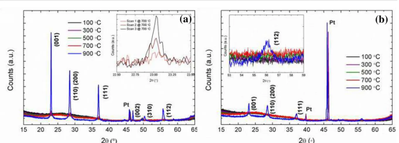
Both thin films were analyzed between 100 and 900 ⁰C with temperature steps of 100 ⁰C and doing 3 consecutive scans at each temperature step. In fig. 4.1, the structural data obtained for these films is shown (curves are presented in steps of 200 ⁰C to simplify the analysis7). As expected for
these dielectrics, only a very broad peak near 2θ=25 ⁰ is visible confirming the amorphous structure of both materials. For Ta2O5, fig. 4.1a, some peaks start to appear at 700 ⁰C and at 900 ⁰C these peaks are
more pronounced, being attributed to β-Ta2O5. In the inset of this figure, the three consecutives scans
for 700 ⁰C are shown which allow confirming that the crystallization starts at this temperature by seeing the increase of the intensity of the peaks in each scan. For TSiO, fig. 4.1b, it would be predictable a higher crystallization temperature due to incorporation of SiO2 – mixing these materials a
structural disorder is induced and, in fact, crystallization only occurs at 900 ⁰C. Both crystallization temperatures are higher than the limitation considered in this work, meaning that amorphous structure is conserved for all the fabricated TFTs.
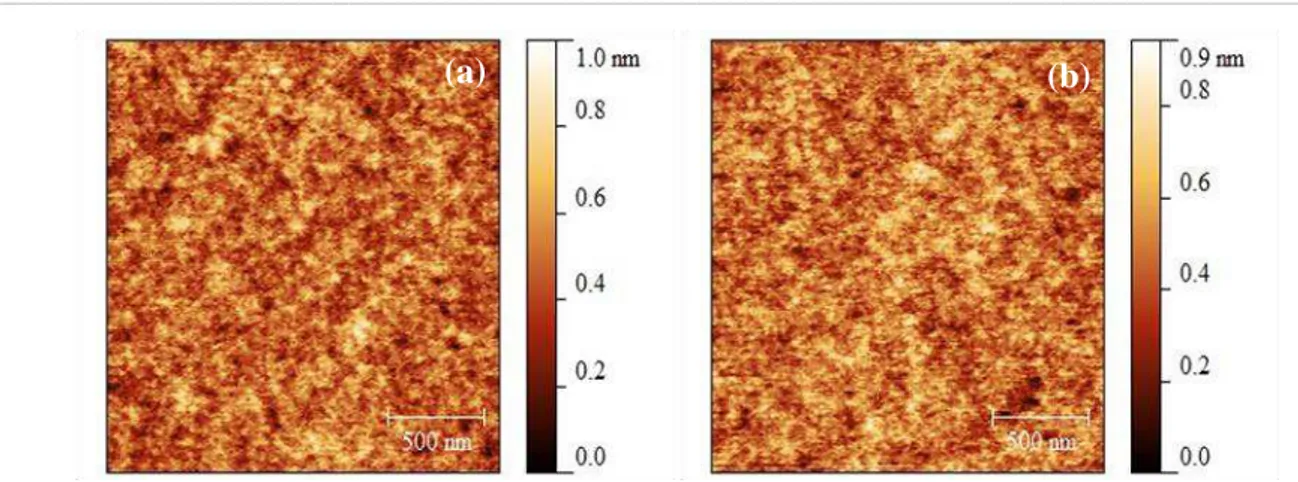
The amorphous structure was confirmed using Atomic Force Microscopy (AFM), as shown in fig. 4.2. It is possible to note that surfaces of both thin films are completely smooth and their roughness very low (close to detection limit of equipment, above 0.1 nm).
An elemental analysis of TSiO thin film was done using Rutherford Backscattering Spectrometry (RBS) technique in Nuclear and Technological Institute (ITN), Portugal. The results
7In both dielectrics a peak at 2θ=46 ⁰ is visible and is due to the Pt foil (the heating element) above which the sample is placed.
(b)
(a)
Figure 4.1 –Diffractogram for Ta2O5 (a) and TSiO (b) thin films, annealed at different temperatures until the
crystallization is evident.The data obtained is compared with the ICSD database and corresponds to
A Second-Order ΣΔ ADC using sputtered IGZO TFTs with multilayer dielectric
__________________________________________________________________________________
13
(a)
(b)
Figure 4.2 - AFM analysis, showing the amorphous structures of Ta2O5 and TSiO thin films.
obtained were fitted, fixing the oxides composition and allowing the system to adjust the stoichiometry (Ta2O5)x(SiO2)y. According to the results, the thin film presents a Ta2O5/SiO2 ratio of
2.2 and an areal density of 1.4×10¹⁸ at/cm2. The thin film thickness measured by profilometer was 225
nm, which means that considering the thickness obtained by RBS, the co-sputtered material presents a density near 6.2×10²² at/cm3. Considering the molar mass (441.9 g/mol), the density of β-Ta
2O5 (8.2
g/cm3) and the number of atoms presents in each molecule of Ta
2O5 (7 atoms), the density of Ta2O5 is
7.8×10²² at/cm3. The density obtained for the TSiO film shows a good match to the theoretical density
of Ta2O5, suggesting a structure with good compactness.
The spectroscopic ellipsometry technique acquires a high importance in dielectrics study. Thin films of Ta2O5 and TSiO on Si were analyzed using it. The Tauc-Lorentz dispersion formula was used
and the best fitting results were obtained for two oscillators, wherein the range of detection of one of them was greater than 6 eV.In fig. 4.3, dependences of refractive index (n) and extinction coefficient (k) on Energy (E) are shown and, in table 4.1, some properties obtained by Tauc-Lorentz dispersion formula are presented.
(a)
(b)
Figure 4.3 - Spectroscopic ellipsometry analysis: comparison between Ta2O5 and TSiO thin films in terms of
A Second-Order ΣΔ ADC using sputtered IGZO TFTs with multilayer dielectric
__________________________________________________________________________________
14 Table 4.1 - Properties of Ta2O5 and TSiO films obtained by Tauc-Lorentz dispersion method.
Sample Thickness (nm) Roughness (nm) Eg (eV)
Ta2O5 267.4 1.1 4.20
TSiO 237.7 0.4 4.23
The positioning of the TSiO plots in fig. 4.3 clearly suggests that SiO2 is incorporated in TSiO,
although the Ta2O5 concentration is considerably higher (TSiO plot closer to Ta2O5 in terms of values
and shape). These results are in agreement with RBS analysis, as shown before. It is noteworthy that due to the usage of substrate bias during thin film deposition, the percentage of SiO2 in film is lower
[9]. Furthermore, the broad peak in n-E plot suggests that samples have an amorphous structure, what is in agreement with previous results of XRD and AFM. In terms of relative density, the refractive index for TSiO is lower indicating that its density is lower comparing to Ta2O5, which is consistent
with RBS analysis. Regarding values of energy that induce absorption in the beginning of conduction band, these are shown in fig. 4.3b. Band gap (Eg) is slightly higher for TSiO than for Ta2O5 film,
suggesting that SiO2 is present in film, but in low percentage. On the other hand, the Eg value even for
Ta2O5 is lower than the typical that is closed to 4.5 eV, which is probably due to sputtering system
(mainly by the usage of substrate bias that induces some differences in film). Other reason found in literature is related to the model used in simulation which considers the tail-states that are inside the Eg
[9]. In terms of roughness, the values obtained indicate a flat surface in accordance with AFM images. Given that the main intent of integrating these dielectrics in TFT structures, it is imperative to analyze several electrical parameters such as κ, breakdown field (EB), capacitance per unit area (Ci)
and current density (J). For this end, metal-insulator-metal (MIM) structures annealed at 150 ⁰C were analyzed, being the results presented in table 4.28. C-V and C-f plots are shown in fig. E.1
(Appendix E).
Table 4.2 – Electrical properties of Ta2O5 and TSiO determined from MIM structures.
Analyzing the electrical properties of films, it is possible to observe a growth tendency of κ for dielectrics with higher Ta concentration. In fact, κ obtained for Ta2O5 is extremely close to the values
reported in literature (approximately 25) [56]. TSiO exhibits a higher EB than Ta2O5 which is highly
relevant to improve TFT and circuit reliability. Reinforcing this, J is considerably lower for the co-sputtering film even with a higher voltage applied.
8 Results for SiO2 films are not presented in this table, given that for the deposition conditions used herein these films always revealed very large leakage current, inhibiting proper parameter extraction.
Sample Thickness (nm)
EB
(MV/cm)
κ Ci
(nF/cm2)
J @ EB max
(A/cm2)
Ta2O5 230.0 1.54 22.6 87.0 1.21×10⁻²
A Second-Order ΣΔ ADC using sputtered IGZO TFTs with multilayer dielectric
__________________________________________________________________________________
15
(a)
(b)
Figure 4.4 - Measured I-V characteristics for devices with W/L=160/20µm/µm and annealed at 200 ⁰C. Effect of dielectric composition and the usage of substrate bias in devices with approximately the same thickness (a) and
of dielectrics thicknesses considering the same material and the usage of substrate bias(b).
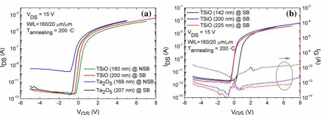
Next step was to integrate these dielectrics in IGZO TFTs. To this end, TFTs with a staggered bottom gate, top-contact configuration were produced using Ta2O5 and TSiO as dielectrics. Several
devices were fabricated varying the dielectric thickness, the usage of substrate bias (with or without substrate bias denoted SB and NSB, respectively) and the annealing temperature (150 or 200 ⁰C)9
Measurement of output and transfer characteristics (static current-voltage) allows acquiring a comprehensive characterization of a TFT. Output characteristics mostly provide a qualitative evaluation, giving information about if saturation is achieved (highly relevant for circuit application) or if there is a significant contact resistance. Transfer characteristics generally provide a more quantitative analysis, making possible to extract important parameters such as on-off ratio, Von,
subthreshold swing (S) and saturation mobility (µsat) [57].
Fig. 4.4a shows the difference in TFT performance taking into account the two dielectrics previously analyzed and the influence of using substrate bias during deposition. Fig. 4.4b presents the influence of dielectric thicknesses on the TFT’s transfer characteristics, considering the amplitude of gate leakage current (IG). The electrical properties of devices depicted in fig. 4.4 are summarized in
table 4.3. The µsat was calculated in the saturation regime. An output curve for one representative
device of this batch is shown in Fig. E.2, Appendix E, being observed that the contact resistance does not have a significant influence in TFT performance considering this channel length (L), the interface IGZO/ Mo and the annealing temperature.
For TFTs with Ta2O5 dielectric a large increase of off-current (which also detrimentally affects
S) is verified for lower dielectric thickness and NSB condition, proving the importance of these parameters to achieve good performance devices. Nevertheless, note that regardless of the processing conditions, Ta2O5-based transistors always present a large variation of properties over a substrate, as
shown in Appendix E. In general, TFTs with TSiO present enhanced properties, particularly a closer to 0 V Von and improved uniformity (in terms of device-to-device variation in the same substrate). Again,
A Second-Order ΣΔ ADC using sputtered IGZO TFTs with multilayer dielectric
__________________________________________________________________________________
16 larger thickness and use of SB are advantageous for transistor performance for TSiO. In fact, when SB is used during a deposition, the molecules that are linked by weak bonds are re-sputtered, decreasing the deposition rates, as shown in introduction of section 4.1. As a result, the molecules linked by strong bonds remain in film turning it denser, providing better insulating properties [9]. This argument is more evident in terms of S, suggesting that when SB is not used the interface dielectric/semiconductor presents worst properties.
In terms of IG, lower values are obtained for thicker dielectrics, as expected (fig. 4.4b).
Furthermore, table 4.3 also shows that the multicomponent approach and the use of substrate bias are able to reduce IG levels when compared to Ta2O5. This indicates that good device reliability can be
obtained by using thinner TSiO films, provided that substrate bias is used.
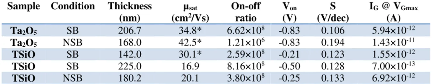
Table 4.3 – Summary of electrical properties of devices annealed at 200 ⁰C using different dielectrics in different conditions, depicted in fig. 4.4.
Sample Condition Thickness (nm)
µsat
(cm2/Vs)
On-off ratio Von (V) S (V/dec)
IG @ VGmax
(A)
Ta2O5 SB 206.7 34.8* 6.62×108 -0.83 0.106 5.94×10⁻¹²
Ta2O5 NSB 168.0 42.5* 1.21×106 -0.83 0.194 1.43×10⁻¹¹
TSiO SB 142.0 30.1* 2.59×108 -0.21 0.123 1.55×10⁻¹²
TSiO SB 225.0 16.9 8.16×10⁸ -0.50 0.128 7.00×10⁻¹³
TSiO NSB 180.2 20.1 3.80×10⁸ -0.25 0.133 6.92×10⁻¹²
* - Given the large size of capacitors available in the mask layouts used in this work, Ta
2O5 MIM structures typically
exhibited large leakage currents, inhibiting a correct determination of Ci. Hence, µSAT for TFTs with Ta2O5 and TSiO should
be overestimated.
Optimized TSiO devices present S in the range of 0.1-0.2 V/dec, on-off ratios exceeding 108 and
µsat>15 cm2/Vs. These results are comparable to state of the art IGZO TFTs with the added advantages
of low operating voltage (enabled by the high-κ), low temperature processing and having the same technique to deposit all the transistor layers.
Another significant characterization technique for TFTs is related to their stability evaluation. In this way, stress measurements using a positive gate bias-stress (VG ≈ 4 V) were realized in devices
annealed at 200 ⁰C, in order to understand the degradation mechanisms and their magnitude depending on the dielectric. Transfer curves for stress and recovery at small VDS, close to 0.1 V, of devices with
Ta2O5 and TSiO dielectrics, deposited using SB, are presented in Fig. E.6 (cf. Appendix E). Fig. 4.5
summarizes the Von and S variations during these stress measurements.
According to literature, there are two mechanisms of instability that can occur in these TFT structures. The first one is related to electron trapping at or near the semiconductor/dielectric interface; the second is associated to the migration of negative ion within dielectric to gate/dielectric interface and the movement of positive ion within dielectric to semiconductor/dielectric interface [29]. Furthermore, the direction of Von shift is imperative to understand the mechanism that is involved. In
fact, the Von shift is directly related to total charge that migrates to the new centroid location of charge.
A Second-Order ΣΔ ADC using sputtered IGZO TFTs with multilayer dielectric
__________________________________________________________________________________
17 Figure 4.5 – Von and S variations during stress and recovery measurements for TFTs annealed at 200 ⁰C using
Ta2O5 and TSiO as dielectric layer for TFTs with W/L = 160/20 µm/µm, applying a gate field of 0.16MV.cm-1 in
dark (a). Solid and open circles denote ΔVon and ΔS, respectively. Mechanisms involved in AOS and dielectric
materials, when a positive gate bias stress is applied in a staggered bottom gate, top contacts structure (b) (adapted from [58]).
(a)
(b)
Some parameters such as light, room temperature, humidity and the air exposition can also change the mechanism and its intensity. However, the complementarity of these different studies is important to understand exactly the mechanism involved and how its magnitude varies according to conditions of measurement. [27]
Fig. 4.5 suggests that the degradation mechanism involved with both dielectrics is associated with ion migration, as a negative ∆Von is verified. This is plausible given the low deposition/annealing temperature of the dielectric layers used here, being the effect more intense for Ta2O5. On the other hand, fig. E.6 in Appendix E, reveals a clockwise hysteresis which is consistent to
electron trapping phenomena. Moreover, the variations in terms of S (Fig. 4.5) and ID (Fig. E.6,
Appendix E) are consistent with the theory that these two mechanisms (ion drift and charge trapping) are concurrent, with the TSiO providing a better equilibrium between both.
In terms of recovery, this “instability” mechanism is reversible – the final Von and S values are
close to the last results obtained without supplying additional energy to the system. Hence, it is plausible to assume that defect creation should not be relevant, as it would typically require a subsequent annealing treatment to enable full recovery [29]. Still, TSiO restores its initial VT faster
than Ta2O5, reinforcing the idea that it is the best choice between these two dielectrics. [58]
In brief, during these studies, it was verified that multicomponent dielectrics, specially using substrate bias during deposition, provide better properties for dielectric layer. In fact, despite the relatively large variation of device properties during stress measurements, TSiO SB provides major advantages over single Ta2O5 layers deposited without substrate bias. Furthermore, the smooth surface