Daniela Ramalho Magalhães
Bachelor in Micro and Nanotechnology Engineering
[Habilitações Académicas]
[Habilitações Académicas]
[Habilitações Académicas]
[Habilitações Académicas]
[Habilitações Académicas]
Influence of uniaxial bending on IGZO TFTs:
A study of materials and device
[Título da Tese]
Master of Science in
Micro and Nanotechnology Engineering
Adviser: Prof. Pedro Barquinha, FCT-UNL
Co-adviser: Dr. André Clausner, IKTS-Fraunhofer
Examination Comitee
Chairperson: Prof. Luís Pereira, FCT-UNL
Influence of uniaxial bending on IGZO TFTs: A study of materials and device
Copyright © Daniela Ramalho Magalhães, Faculdade de Ciências e Tecnologia,
Universidade Nova de Lisboa.
A Faculdade de Ciências e Tecnologia e a Universidade Nova de Lisboa têm o
direito, perpétuo e sem limites geográficos, de arquivar e publicar esta dissertação
“The best way out is always through”
Acknowledgment
Finalmente acabou uma longa etapa que só foi possível concretizar por toda ajuda que me foi oferecida durante todos estes anos e especialmente durante a concretização deste trabalho. Em primeiro lugar quero agradecer à minha instituição, a Faculdade de Ciências e Tecnologia da Universidade Nova de Lisboa, e ao Departamento de Ciências de Materiais que me fizeram crescer como pessoa e como estudante.
Queria também agradecer ao professor Rodrigo Martins e à professora Elvira Fortunato pois sem eles não existiria a oportunidade de me formar no curso de Engenharia de Micro e Nanotecnologia, nem a possibilidade de desenvolver os meus conhecimentos num lugar tão prestigiado como o CENIMAT. Além disso também gostaria de agradecer a disponibilidade de poder concretizar parte do meu trabalho na Alemanha.
Um especial agradecimento ao meu orientador professor Dr. Pedro Barquinha, por se ter disponibilizado a orientar o meu trabalho e por ter sempre mostrado confiança no meu trabalho e principalmente por ter acreditado em mim, foi sem dúvida uma das pessoas mais importantes neste trabalho.
Thank you to everyone in IKTS-Fraunhofer for helping me during this time in a different place. To Prof. Dr. Ehrenfried Zschech for allowing me to spend time in this institution and specially to Dr. André Clausner for helping me when I was in Dresden and in Portugal. To Dr. Martin Gall and Dr. Jürgen Gluch for always helping and for the guidance that they provided. Thank you to Alexander Than, Zhongquan Liao, Yvonne Standke, Dr. Rüdiger Rosenkranz and Friederich Schmid for taking some time of their schedule to help me characterize some of the systems. A special thank you to Aránzazu Garitagoitia Cid for being a friend since the beginning and being interested in my work and well-being, and to Simon for all the conversation and beer. Danke schön! Obrigada também ao meu amigo Viorel que sempre me acompanhou e fez companhia enquanto estávamos num lugar diferente.
A toda a equipa do CENIMAT pelo bom ambiente e espírito de entreajuda, obrigada à professora Dra Joana Pinto por sempre ter tirado uns minutinhos para falar comigo quando precisava. Um especial agradecimento à Ana Santa, ao Trigo, à Inês e à Cátia por se terem disponibilizado a ajudar me, sem vocês isto não teria sido possível. Aos restantes colegas do open space, um grande obrigado pela diversão e ajuda que sempre disponibilizaram. Em especial, à Sara pelos cafés, boleias e conversas intermináveis e ao Jolu pelos cafés e pelas reclamações. Um abraço a todos. Um obrigado a todos os meus colegas e amigos do curso. Em especial á Ana por sempre me ter dado companhia e ajudado durante todos estes anos e por seres uma das minhas melhores amigas., um obrigado também ao Fernas por ser sempre amigo e colega de trabalho excecional e à Caupi, grande amiga da margem sul e colega.
Abstract
In recent years flexible electronics have gained relevance with applications such as displays, sensors and wearables. In that regard, studying how flexible transistors behave under bending has become of major importance. This work aims to fabricate indium gallium zinc oxide (IGZO) Thin Film Transistors (TFT) with the best bendability possible, without any major changes in the production techniques already used in the industry.
To understand the influence of the substrate on flexible devices, TFTs were fabricated on polyimide substrates using different thicknesses, down to 25 μm, with and without parylene encapsulation layers on top of the device stack. To determine the position of the neutral strain plane, nanoindentation measurements were performed on different device layers at IKTS-Fraunhofer, within BET-EU project.
The delamination of the substrates is a critical step, especially for thinner substrates. The concept of “paper blade” was used in this project to improve the yield of the delamination process. Initial bending measurements, using a 75 μm thick substrate, showed that bending radii of 45, 25 and 15 mm do not permanently change the performance of the TFTs. Tensile bending measurements with a radius of 1.25 mm were also performed, revealing that the 75 μm thick substrate achieves critical failure in <500 cycles, while the thinner substrate (25 μm) could withstand almost 1000 cycles.
The most common failure mechanism observed under tensile bending was the appearance of cracks in the oxide dielectric when in direct contact with the polyimide substrate. These cracks do not appear in regions where molybdenum gates were in contact with the substrate, hence the mismatch between the coefficient of thermal expansion of the substrate and the dielectric thin film were identified as the reason for failure.
This work shows that, even with intrinsically rigid materials as oxides and metals, it is possible to obtain reliable flexible TFTs, provided that proper stack engineering is considered for their fabrication.
Keywords: flexible electronics, IGZO TFTs, bending, mechanical characterisation, neutral strain
Resumo
Atualmente, a eletrónica flexível tem ganho maior relevância com aplicações como mostradores, sensores e wearables. Devido a isso, os estudos do comportamento de transístores flexíveis quando estão dobrados é extremamente importante. Este trabalho tem como objetivo fabricar transístores de filme finos (TFT) de óxido de índio-gálio-zinco (IGZO) com a melhor flexibilidade possível, sem alterar significativamente as técnicas de produção utilizadas atualmente pela indústria.
Para compreender a influência do substrato em dispositivos flexíveis, foram fabricados TFTs em substratos de poliamida com espessuras até 25 μm, com e sem uma camada de encapsulamento de parileno. Para a determinação do plano de deformação neutra, foram efetuados testes de nanoidentação em diferentes camadas constituintes dos dispositivos pelo IKTS-Fraunhofer, incluído no projecto BET-EU.
A delaminação dos substratos mostrou-se uma etapa crítica, especialmente para substratos mais finos. O conceito de “lâmina de papel” foi utilizado neste trabalho para aumentar o rendimento do processo.
Medições iniciais dos dispositivos fabricados num substrato com 75 μm, a sofrer deformação mecânica em tensão e compressão, mostram que raios de curvatura de 45, 25 e 15 mm não afetam permanentemente o desempenho dos TFTs. Testes de deformação tênsil com um raio de curvatura de 1.25 mm também foram realizados, mostrando que os dispositivos fabricados no substrato de 75 μm de espessura atingem falha crítica em <500 ciclos, enquanto que o substrato mais fino (25 μm) consegue alcançar quase 1000 ciclos.
O mecanismo de falha ocorrido durante a deformação mecânica em tensão dos dispositivos foi o aparecimento de fendas, onde o dielétrico se encontrava em contacto com o substrato de poliamida. Estas fendas não ocorrem em regiões onde os elétrodos de portas de molibdénio estão em contacto com o substrato, concluindo-se então que a principal razão para a ocorrência desta falha deve-se à diferença entre coeficientes de expansão térmica do substrato e do filme dielétrico. Este trabalho mostra que é possível obter TFTs flexíveis e fiáveis, mesmo utilizando materiais intrinsecamente rígidos como óxidos e metais, desde que se tenha em conta uma boa engenharia e estudo de multicamadas para a fabricação.
Palavras chave: eletrónica flexível, IGZO TFTs, curvatura, caracterização mecânica, plano de
Abbreviations
AMLCD Active Matrix Liquid Crystal Display
AMOLED Active Matrix Organic Light Emission Diode
CEMOP Centro de Excelência em Microeletrónica, Optoelectrónica e Processos
CENIMAT Centro de Investigação de Materiais
CTE Constant of Thermal Expansion
EDS Energy-dispersive X-ray spectroscopy
e-skin Electronic skin
IGZO Indium Galium Zinc Oxide
IKTS Fraunhofer Institut für Keramische Technologien und Systeme Fraunhofer K25 Kapton with thickness 25 μm
K50 Kapton with thickness 50 μm
K75 Kapton with thickness 75 μm
NSP Neutral Strain Plane/Point
PEN Polyethylene Naphthalate
PET Polyethylene Terephthalate
PI Polyimide
PVD Physical Vapour Deposition
RF Radio Frequency
RIE Reactive Ion Etching
SE Secondary Electrons
SEM Scanning Electron Microscope
SEM-FIB Scanning Electron Microscope – Focused Ion Beam
TEM Transmission Electron Microscope
TFT Thin Film Transistor
Symbols
b position of NSP
Ci Intrinsic capacitance
d crystal lattice distance
df film thickness
ds substrate thickness
ID Drain Current
IG Gate Current
Ion/Ioff Ratio between On Current and Off Current
L Channel Length
n number of layers
R Bending Radius
R0 Radius at unstressed state
Tg Vitreous Transition Temperature
ti thickness of individual layer
tj sum of thickness of all layers before individual layer
VDS Voltage between drain and source
VGS Voltage between gate and source
Von Turn-on Voltage
VT Threshold voltage
W Channel width
Y Young Modulus
Yf film Young Modulus
Yi individual layer’s Young Modulus
Ys substrate Young Modulus
z distance from the neutral plane
α coefficient of thermal expansion
Table of Contents
1 Motivation and Objectives ... 1
2 Flexible Electronics ... 3
2.1 Thin Film Transistors ... 3
2.2 Mechanical Properties ... 4
2.2.1 Substrates of Choice for Flexible Electronics ... 5
2.2.2 Compression and Tension ... 5
2.2.3 Improving Mechanical Properties ... 6
3 Materials and Methods ... 9
3.1 Fabrication Process ... 9
3.1.1 Materials ... 9
3.1.2 Thin Film Transistors ... 9
3.2 Characterisation Methods ... 10
4 Results and Discussion ... 11
4.1 Multilayer Properties ... 11
4.2 Mechanical Properties of Individual Layers ... 13
4.2.1 Molybdenum and IGZO Layers ... 13
4.2.2 Parylene Layer ... 15
4.3 Flexible Transistors ... 15
4.3.1 Kapton as a Substrate ... 16
4.3.2 IGZO TFTs ... 17
4.3.3 Iddle shelf Time ... 18
4.3.4 Peel-Off (Metal Blade) ... 20
4.3.5 Bending ... 21
4.3.6 Substrate Peel-off ... 23
4.3.7 Cycles of Bending ... 26
5 Conclusions and Future Perspectives ... 33
Appendix A ... 41
Appendix B ... 43
List of Figures
Figure 1-1: Market Forecast for Asia Pacific Flexible Electronics Market by Application (Consumer
Electronics, Automotive, Healthcare, Industrial) (USD Million) until 2024 [3]. ______________________ 1
Figure 2-1: Characteristic curves of transistors: (a) transfer curves; (b) output characteristics [33]. _____ 3
Figure 2-2: Stress vs Strain graph of a material: A defines the elastic limit, B defines the upper yield stress
point, C is the lower yield stress point, D is the ultimate stress point, and E is the breaking or rupture
point [35]. ____________________________________________________________________________ 4
Figure 2-3: Graphical representation of TFTs under uniaxial strain, (a) under compression, (b) under
tension [19]. __________________________________________________________________________ 5
Figure 2-4: General failure mechanisms (a) under tension; (b) under compression [41]. ______________ 5
Figure 2-5: Examples of state of the art methods for better TFT flexibility: (a) double gate TFT
structures [42]; (b) nanowires [43]; (c) mesh and strip pattering layers [44]. _______________________ 6
Figure 2-6: Schematic of a bended system used to understand the equation 4, the top layer is under
tensile strain and the bottom layer is under compressive strain [40]. _____________________________ 6
Figure 4-1: Multilayer System of the TFT: (a) TEM image; (b) schematic of the cross-section of the TFT. 11
Figure 4-2: TEM image of the multilayer system: (a) without annealing; (b) with annealing at 180 °C for 1
hour. _______________________________________________________________________________ 11
Figure 4-3: In-situ XRD of molybdenum under heating from 30 °C to 200 °C. ______________________ 12
Figure 4-4: Nanoindentation measurements for Young Modulus and hardness: (a) Young modulus of
IGZO as deposited, annealed at 140 °C and annealed at 180 °C; (b) Young modulus of molybdenum as
deposited, annealed at 140 °C and annealed at 180 °C; (c) hardness of IGZO at the same temperatures;
(d) hardness of Mo at the same temperatures. _____________________________________________ 13
Figure 4-5: XRD of molybdenum sample as deposited (black) and after annealing (red). ____________ 14
Figure 4-6: Wedge indent on multilayer with 1 m parylene passivation (a) as deposited; (b) annealed at 180 ºC. _____________________________________________________________________________ 15
Figure 4-7: Optical microscope Images of Mo on PEN: (a) 10 cycles with bending radius of 2.5 mm; (b) 1
cycles with bending radius of 1.25 mm. ___________________________________________________ 15
Figure 4-8: Strain on top of Mo depending on the bending radii: in black is K25, in red is K50, in blue is
K75, and in pink is PEN with 125 μm. _____________________________________________________ 16
Figure 4-9: Optical microscope image of the TFTs fabricated on (a) glass substrate; (b) Kapton substrate.
___________________________________________________________________________________ 16
xxii Influence of uniaxial bending on IGZO TFTs: A study of materials and device Figure 4-14: Characteristic curves of TFTs fabricated on a K75 glued to carrier substrate (black), after
delamination (red) and after delamination and annealing (blue): (a) Transfer characteristic curve, and (b)
output characteristic curve. _____________________________________________________________ 20
Figure 4-15: Position of channel regarding the bending direction: (a) channel length perpendicular to
bending direction; (b) channel length parallel to bending direction [70]. _________________________ 21
Figure 4-16: Characteristic curves of TFTs under bending with radii of 45, 25 and 15 mm: (a) transfer
curve for TFTs with channel perpendicular to bending direction; (b) transfer curve for TFTs with channel
parallel to bending direction ____________________________________________________________ 22
Figure 4-17: SEM images of the K25 delaminated sample: (a) surface with the SE2 detector, (b)
cross-section of crack in TFT. _________________________________________________________________ 24
Figure 4-18: Characteristic curves of a TFT in the K25 sample before and after delamination, with probes
on TFTs: (a) Transfer curve; (b) Output characteristic curve. ___________________________________ 24
Figure 4-19: Optical microscope images of the K25 sample after delamination: (a) without parylene layer;
(b) with 5 μm parylene layer.____________________________________________________________ 25
Figure 4-20: Optical microscope images of the K25 sample after delamination: (a) with a metal blade; (b)
with a paper blade. ___________________________________________________________________ 25
Figure 4-21: Transfer characteristic curve of a TFT on a K25 substrate in a flat position, after bending for
10 s with a radius of 10 mm, 5mm, 2.5 mm and 1.25mm _____________________________________ 26
Figure 4-22: Optical microscope image of: (a) K25 sample with 500 cycles of 1.25 mm radius tensile
bending, and (b) K75 sample with 500 cycles of 1.25 mm radius tensile bending. __________________ 26
Figure 4-23: Optical microscope images of K25 sample under tensile bending with 1.25 mm from 0 to
2000 cycles. _________________________________________________________________________ 27
Figure 4-24: SEM images of two different K25 patterned sample: (a) after delamination with metal blade;
(b) after delamination with paper blade and 2000 cycles of 1.25 mm radius of curvature. ___________ 27
Figure 4-25:Characteristic curves of a TFT in the K25 sample before (black) , after delamination (red) with
50 cycles of tensile bending with r= 5mm (blue) and 150 cycles of tensile bending (pink) (a) Transfer curve
of TFT with channel parallel to bending direction; (b) Transfer curve of TFT with channel perpendicular to
bending direction; (c) Output characteristic curve of TFT with channel parallel to bending direction¸ (d)
Output characteristic curve of TFT with channel perpendicular to bending direction _______________ 29
Figure A-0-1:Glueing substrate on a rigid carrier (glass) with a resin ____________________________ 41
Figure A-0-2: Schematic of the fabrication of the IGZO-TFTs used in this work ____________________ 41
Figure B-1: Design of part to adapt to bending machine to achieve bending radius of r=1.25 mm _____ 43
Figure B-2: 3 point bending system (a) picture from the front of the system (a) picture from top of the
system _____________________________________________________________________________ 43
Figure C-1: TEM EDS of the individual layers on the multilayer system of the TFTs studied; (a) Mo; (b)
IGZO; (c) SiO2 (part of multilayer); (d) TaSiO (part of multilayer). _______________________________ 45
Figure D-1: TEM image of the multilayer system with a parylene passivation layer, (a) without annealing;
(b) with annealing at 180ºC for 1 hour ____________________________________________________ 47
Figure E-1:3D surface measurements of the Kapton substrate with 75 μm. _______________________ 49
Figure E-2:3D surface measurements of the Kapton substrate (a) with 50 μm. ____________________ 49
Figure E-3:3D surface measurements of the Kapton substrate with 25 μm. _______________________ 50
Figure F-1: Fabricated TFTs during bending (a) Tension; (b) Compression with a bending 25 mm bending
Figure H-1: Characteristic Curves of TFTs under bending with radii 25 mm and 15 mm and in tension and
compression, in a random ordering of the conditions ________________________________________ 55
Figure H-2: Transfer characteristic curves of TFTs done consecutively in flat condition ______________ 55
Figure I-1: Optical microscope images of the K75 sample after delamination (a) pads; (b) pads with
cracks. ______________________________________________________________________________ 57
Figure I-2: Optical microscope images of K50 and K25 samples after delamination; (a) K50 sample
transistors; (b) K50 vias; (c) K25 sample transistors; (d) K25 sample vias _________________________ 57
Figure I-3: Optical microscope images of the K25 sample with the representation of the location of
probes when measuring TFT characteristic curves; (a) in pads, for gate probe; (b) Transistor, for drain
List of Tables
Table 2-1: Comparison between results obtained from different works considering substrate thickness
and bending radius obtained before critical failure ___________________________________________ 7
Table 4-1: Coefficient of thermal expansion of the different layers in the TFT multilayer structure. ____ 12
Table 4-2: Young Modulus and Hardness obtained with nanoindentation in 400 nm thick IGZO and
Molybdenum Layers, as deposited, annealed 1 hour at 140 °C and annealed 1 hour at 180 °C. _______ 14
Table 4-3: Roughness values for samples K75, K50 and K25. ___________________________________ 17
Table 4-4: Summary of IGZO TFTs parameters, in glass and polymer substrates.___________________ 18
Table 4-5: Summary of IGZO TFTs parameters fabricated on Corning glass after production and after
three weeks, in an oxygen rich environment. _______________________________________________ 19
Table 4-6: Summary of IGZO TFTs parameters fabricated on Kapton substrate (25 um), after production
and after one month in an oxygenated atmosphere. _________________________________________ 20
Table 4-7: Summary of IGZO TFTs parameters, in the K75 substrate, before delamination, after
delamination, and delamination and annealing. ____________________________________________ 21
Table 4-8:Summary of IGZO TFTs, fabricated on the K75 substrate in bending and flat conditions, with
radii 45, 25 and 15 mm ________________________________________________________________ 23
Table 4-9: Summary of IGZO TFTs with channel parallel to bending direction, fabricated on the K25
substrate, in the carrier, after delamination and with 50 and 150 cycles of bending with a radius of 5
mm. _______________________________________________________________________________ 30
Table 4-10: Summary of IGZO TFTs with channel perpendicular to bending direction, fabricated on the
K25 substrate, in the carrier, after delamination and with 50 and 150 cycles of bending with a radius of 5
mm. _______________________________________________________________________________ 30
Table 4-11:Thickness and Young modulus of each layer of the TFT. _____________________________ 31
Table 4-12: Position of the NSP according to parylene thickness, for K25 substrate. ________________ 31
Table G-1: Summary of IGZO TFTs with channel perpendicular to bending direction, fabricated on the K75
substrate in bending and flat conditions, with radii 45, 25 and 15 cm. ___________________________ 53
Table G-2: Summary of IGZO TFTs with channel parallel to bending direction, fabricated on the K75
1
Motivation and Objectives
The flexible electronics sector is now starting to gain momentum, particularly with the investment, by the consumer electronics industry, in flexible and curved phones and wearables. The benefits offered by this type of electronics with respect to weight, cost, ruggedness and portability make it a desirable area to invest [1, 2]. According to Grand View Research [3], it is forecasted that by 2024 the global flexible market will reach USD 87.21 billion globally. The growing trend in the Asia Pacific is shown in Figure 1-1, as an example.
Figure 1-1: Market Forecast for Asia Pacific Flexible Electronics Market by Application (Consumer Electronics, Automotive, Healthcare, Industrial) (USD Million) until 2024 [3].
This work seeks to explore some of the characteristics of inorganic metal-oxide semiconductor thin film transistors (TFT) in flexible polymers under mechanical uniaxial strain, and it is inserted in the BET-EU European Project (http://www.bet-eu.eu) [4].
The main goal of this thesis is to fabricate TFTs with the best bendability possible, studying its layers mechanically and identifying critical ones. This is important because of the many advantages obtained with flexible electronics, with applications such as flexible TFTs [5, 6], bendable and rollable displays, flexible sensors [7, 8], RF tags [9, 10], electronic skin (e-skin) [11], and flexible solar cells [12]. To reach the already defined goals, several fabrication and characterisation techniques were employed, such as,
• Fabrication: sputtering, lithography, reactive ion etching (RIE), and lift off;
2
Flexible Electronics
Flexible electronics have gained more interest in the last years, with applications such as paper-like displays [13, 14], sensors/actuators [15], medical devices [16, 17], and radio frequency (RF) tags [9]. In the future, many electronic assemblies on rigid substrates will be replaced by mechanically flexible or even stretchable alternatives. The reason for this replacement is the qualities that flexibility can offer, such as bendability, conformability and elasticity, making flexible electronics generally lightweight, non-breakable, roll-to-roll and large area manufacturable [12, 16].
In the display industry, this trend is now starting, with LG creating a rollable television [18], and with curved displays already on the market. To achieve device flexibility, it is required the use of flexible components. In microelectronics, one of the most important building blocks is transistors. In this field, TFTs are gaining increasing interest due to ease of manufacture and low-temperature deposition compatible with polymer substrates [19]. These devices allow the drive of active matrix liquid crystals displays (AMLCDs) [20], and active matrix organic light emission diode (AMOLED) [14, 21]. However, they are also being used in applications such as X-ray [22, 23], temperature [24] and pH sensors [25, 26], wearable electronics, e-skin and memories [27].
2.1
Thin Film Transistors
A TFT is a field-effect transistor fabricated by depositing thin films of the constituent layers over a non-conducting substrate. These layers consist of an active semiconductor layer, the dielectric layer and metallic contacts. The semiconductor layer can be amorphous silicon, more conventionally used and well established, or an amorphous metal oxide semiconductor, which, although not as well established, can have good uniformity over large areas, is low temperature manufacturable, transparent, and can achieve mobilities much higher than amorphous silicon [28]. For the metal-oxide semiconductors, the indium gallium zinc oxide (IGZO) stands out as the most favourable material for oxide TFT applications, since it presents several advantages, such as high mobility, wide process window, and superior stability [29, 30].
Thin film transistors have different configurations regarding the position of the channel with respect to the metal contacts, staggered or coplanar, and regarding the position of the gate, being top or bottom gate. This creates four different configurations, each with its own set of advantages and disadvantages [31]. Complying with the most widely used configuration in display industry, this work will study staggered bottom-gate TFTs.
2.1.1
Operation of a TFT
4 Influence of uniaxial bending on IGZO TFTs: A study of materials and device
When the transistor is in the off-state, the obtained current ID is very small, since the low or negative VGS (considering a n-type transistor) is unable to induce significant free charge accumulation close to the dielectric/semiconductor interface. The off state is then characterised as being the current before Von [32].
When the transistor is in the on-state, different operation regimes can be distinguished depending on the value of VDS. When VDS<VGS-VT, the TFT is in the pre-pinch-off regime (or linear regime for VDS≪ VGS-VT). When VDS> VGS-VT, the accumulation layer close to the drain region becomes depleted, leading to the saturation of ID, known as saturation regime [32].
{𝐼𝐷= 𝐶𝑖𝜇𝐹𝐸 𝑊
𝐿 [(𝑉𝐺𝑆− 𝑉𝑇)𝑉𝐷𝑆− 1
2 𝑉𝐷𝑆2 ] 𝑖𝑓 VDS< VGS− VT 𝐼𝐷= 𝐶𝑖𝜇𝑠𝑎𝑡𝑊𝐿 (𝑉𝐺𝑆− 𝑉𝑇)2 𝑖𝑓 VDS> VGS− VT
(1)
(2)
In equations 1 and 2, ID is the drain current, Ci is the intrinsic capacitance, μFE is the field effect mobility, μsat is the saturation mobility, VGS is the gate voltage, VT is the threshold voltage, VDS is the drain voltage, and W and L are the width and length of the channel, respectively.
2.2
Mechanical Properties
When an external force is applied to an object made of elastic materials, it changes the shape and size of the object, making it is possible to measure the strain and the stress associated. The strain is the relative change in shape or size of an object due to externally applied forces (dimensionless), and stress is the internal force (per unit area) associated with strain (Force per unit length) [34].
For flexible electronics, where the mechanical bending is a required function, the mechanical properties of the constituent layers are very important to consider when projecting a device. In this case, the most important mechanical properties are the ones that define the elastic region, such as the Young modulus, since the device needs to be restored to its original position after mechanical stress. However, for plastics, it is also necessary to consider viscosity, creep rate and damping. Mechanical properties, such as hardness, fracture strength, fatigue resistance and wear, define the plastic region and are important to understand the failure of the device [34]. Figure 2-2 shows the relationship between strain and stress where the plastic and elastic regions are evidenced.
Figure 2-2: Stress vs Strain graph of a material: A defines the elastic limit, B defines the upper yield stress point, C is the lower yield stress point, D is the ultimate stress point, and E is the breaking or rupture point [35].
Within the elastic region, Hooke’s law (in Figure 2-2, from 0 to A) relates the behaviour between the strain and the stress, as shown in equation 3, where σ is the stress, ε is the strain, and Y is the Young Modulus [34]. This way, it is possible to obtain the Young modulus by its slope.
𝜎 = 𝑌𝜀 (3)
thermal expansion between bonded elements when temperature changes, piezoelectric response to
an electric field, electrostatic forces, gravitational or inertial forces, compositional segregation by bulk diffusion, electromigration, chemical reactions, stress-induced phase transformations, and plastic or creep deformation [36].
2.2.1
Substrates of Choice for Flexible Electronics
Plastic or thin metal foils are the most widely chosen substrates for flexible electronics, having the thickness and conformability necessary for these applications [37]. However, it is possible to obtain flexible devices, like curved displays, from a very thin glass [38].
Polymeric foils are extremely attractive, since they can be made lightweight and low cost. The most used ones are polyethylene terephthalate (PET), polyethylene naphthalate (PEN), and polyimide (PI) [19, 37]. In the last years, PI has been the polymer of choice for the substrate in ultra-flexible devices. Its properties, such as a very low (CTE) coefficient of thermal expansion, a high glass transition temperature (Tg), as high as 300 °C, and the possibility of fabricating this layer by spin coating, makes it the best choice for the basis of these devices [39].
2.2.2
Compression and Tension
Bendability and conformability are important requirements for flexible electronic systems. As such, it is imperative to study the mechanical behaviour of the samples composing these systems. Bending can be uniaxial or biaxial. In the former, the sample is bent in one direction and the sample suffers tension or compression, while for the latter, the sample is subjected to strain in two directions [40].
For this work, only the uniaxial bending is considered. The uniaxial strain can be compressive or tensile, depending on the position of the sample in the bending environment, as shown in Figure 2-3 (a) and Figure 2-3 (b), respectively.
Figure 2-3: Graphical representation of TFTs under uniaxial strain, (a) under compression, (b) under tension [19].
These two different bending conditions give rise to different problems in the devices. Commonly, thin films subjected to compression fail due to debonding and delamination, Figure 2-4 (a), caused by poor
adhesion between the constituent layers of the device. When subjected to , the main failure is
6 Influence of uniaxial bending on IGZO TFTs: A study of materials and device
strain necessary for definitive mechanical failure is much higher in compression than tension, around 0.3 % for tension [41].
2.2.3
Improving Mechanical Properties
Since TFTs have a critical strain, attempts have been done to reach the critical strain at increasingly smaller radii. Some simple methods to achieve ultra-flexibility are the use of thinner substrates, the choice for the constituent layers with smaller Young modulus and passivation layers.
State of the art methods includes double gate TFT structures [42], nanowires[43], mesh and strip patterning layers [44], seen in Figure 2-5, and locating the TFTs close to the neutral bending plane [45].
Figure 2-5: Examples of state of the art methods for better TFT flexibility: (a) double gate TFT structures [42]; (b) nanowires [43]; (c) mesh and strip pattering layers [44].
2.2.3.1
Substrate Thickness
In microelectronic and nanoelectronic devices, the substrate’s thickness is generally a lot higher than the one of the film or device, meaning it is the most important characteristic for achieving lower bending radius, as shown in equation 4.
Figure 2-6: Schematic of a bended system used to understand the equation 4, the top layer is under tensile strain and the bottom layer is under compressive strain [40].
Young modulus (Y) can be used to determine the strain (ε) experienced by any TFT device as a function of bending radius and film thickness, shown below, where the position of the top and bottom layer is schematised in Figure 2-6,
𝜀𝑠𝑢𝑟𝑓𝑎𝑐𝑒 = (𝑅 ±1 𝑅1
0) .
𝑑𝑠+ 𝑑𝑓1+ 𝑑𝑓2
2 .
𝜒(𝜂12+ 𝜂22) + 2(𝜒𝜂1+ 𝜒𝜂1𝜂2+ 𝜂2) + 1
𝜒(𝜂1+ 𝜂2)2+ (𝜂1+ 𝜂2)(1 + 1𝜒) + 1
(4)
where R is the radius of curvature, R0 is the radius of curvature of the structure before applying any external bending moment, and χ = Yf /Ysη1 = df1/ds and η2 = df2/ds, characterize the top or bottom surface of the substrate, respectively. Likewise, ds, df1, and df2 are, respectively, the thicknesses of substrate, stiff film on top, and stiff film on bottom. When decreasing ds, keeping all the other parameters constant, ϵsurface also decreases.
In conclusion, with decreasing R and increasing ds, the strain εsurface increases.
2.2.3.2
Neutral Strain Plane
A common method for improving the mechanical performance of TFTs is by introducing a passivation layer to achieve the neutral strain plane. In theory, if one sandwiches the TFTs between two equal layers of thin films, the tension and compression forces exerted on the bottom substrate will be annulled by the top substrate. This means that the tension and/or compression forces exerted during the bending will not have any influence on the devices they are protecting.
The position b of the neutral mechanical plane (NMP), zero strain position of a multilayer stack with the nth layer on top of the substrate at the bottom, is given by [45],
b =∑ Yiti[∑ tj− t
i
2
i
j=1 ]
n i=1
∑ Yni=1 iti (5)
where n is the number of layers, Yi is the Young modulus, ti is the thickness of each individual layer and tj is the sum of thickness of all layers before individual layer.
Even if the neutral strain point can be determined, it is generally known that if one puts a passivation layer of the same thickness on top of the stack, the NMP is much closer to the stack and the strain is reduced. However, to get the smallest bending possible, it is essential to know the weakest layer, and ideally put the neutral mechanical plane in that layer.
For the calculation of the engineering strain εeng using the NSP position the equation 6 can be used,
𝜀eng=Rz (6)
where R varies linearly with the distance z from the neutral plane, where z is the distance between the position where we want to calculate the strain, generally the last layer of the device, and the NMP position,b.
2.2.3.3
Bending radius obtained for TFTs
In the last years, studies have been performed to analyse the smaller bending radius obtained for IGZO - TFTs. Table 2-1 summarizes some of the results obtained in other works for TFTs.
Table 2-1: Comparison between results obtained from different works considering substrate thickness and bending radius obtained before critical failure
substrate Bending mode Bending radius (mm) reference
50 μm PI tensile 5 Petti et al, 2015 [46]
3
Materials and Methods
3.1
Fabrication Process
To accomplish the established goals, two different types of samples were fabricated: firstly, samples of unpatterned layers of Mo, IGZO, parylene and the TFT multilayer, deposited on glass and polymeric substrates; secondly, samples of working TFTs, deposited on polyimide and glass substrates, as term of comparison, analysing polymer’s effect on the TFT.
3.1.1
Materials
The used substrates were Corning Eagle XG glass (1 mm thick), PEN Q51 (125 μm thick), and Kapton HN with three different thicknesses (75, 50 and 25 μm), the last two being from Dupont. The molybdenum layer was deposited in a RF Magnetron Sputtering PVD AJA ATC 1800S, with a molybdenum target from AJA International. The IGZO, from AJA International with composition 1:1:1 (In2O3:Ga2O3:ZnO molar ratio), and the dielectric multilayers were deposited in a deposition system RF magnetron sputtering PVDAJA ATC 1300F. The multilayer dielectric was deposited using Ta2O5 and SiO2 targets from AJA International. The parylene C was deposited from a Specialty Coating System Model PDS 2010 Labcoter 2 [51].
3.1.2
Thin Film Transistors
The first step for fabricating the TFTs is annealing, at 180 °C during 1 hour, of the polymeric substrate while free standing. The primary reason for this thermal treatment is the removal of residual stresses, strains and shrinkage of the polymer foils before processing to mitigate the layer-to-layer misalignment [52, 53].
After the annealing, the polymer substrate is glued to a carrier glass. The glue is a resin that is spin coated on to the glass, and after it has the substrate on top is cured. This step is necessary because it allows an easier handling of the sample during processing, and for a better uniformity of the deposited layers.
After the substrate is glued to the carrier glass, the substrate is once again annealed at 180 °C for 1 hour, and cleaned in ultrasounds for 15 minutes, with acetone and isopropyl alcohol. After this step, the substrate is once again heated at 120 °C for 20 minutes, to ensure that any cleaning agent is evaporated from the substrate.
10 Influence of uniaxial bending on IGZO TFTs: A study of materials and device To pattern the last contacts, source and drain, a Mo layer was used. The deposition and etching are done similarly to the gate electrodes [54].
For the passivation of the K75 and K25 samples, 1.8 g, 9 g and 40 g parylene layers are deposited on the parylene system, to achieve thicknesses of 1 μm and 5 μm and 22 μm, respectively. A schematic of the fabrication steps of these devices can be seen in Figure A-0-1and Figure A-0-2
3.2
Characterisation Methods
This work includes the study of TFT’s mechanical behaviour and influence on bending conditions and electrical and mechanical characteristics of the devices.
For samples characterisation, a broad range of tools were used, aiming to study their structural, morphological, compositional, optical, electrical and mechanical properties. Among these, the compositional, structural and mechanical analyses of the individual layers, as well as the multilayer system, were performed at IKTS-Fraunhofer, in the framework of the BET-EU European project.
The samples’ mechanical characterisation was done by nanoindentation, using system Hysitron TI 950 Triboindenter®. For the simple nanoindentation experiment, where simple mechanical properties of the layers, such as Young Modulus and Hardness, can be acquired, individual samples of 2.5 × 2.5 cm of glass with Mo (400 nm), IGZO (400 nm), Parylene (500 nm and 1 μm) were used and indented with a Berkovitch tip. These samples were also annealed at 140 ºC and 180 ºC, to understand how the temperature influences the mechanical properties of the individual layers. Delamination experiments were also performed on the multilayer samples on the glass with a wedge indent. Cross sections of the indents were performed in a Carl Zeiss SEM/FIB NVision 40.
A Carl Zeiss Libra 200 TEM with EDS was used to understand the structure of the multilayers and the influence of temperature on the multilayer structure. Regarding TEM characterisation, lamellas of the samples with a very small thickness were produced, using an FEI Helios NanoLabTM 660 SEM.
The calculation of the coefficient of thermal expansion of the polybdenum was deposited on silicon with 400 nm thickness.
The roughness of the polyimide substrates was calculated from the 3D scanning of the surface of the substrates with a profilometer, Ambios XP-Plus 200 Stylus, where the scanning of the sample was achieved on an area of 0.5 mm × 0.5 mm with a space of 0.3 μm between lines. The samples were on a glass support with Kapton tape.
The electrical characteristics of the TFTs were obtained using a semiconductor parameters analyser (Agilent 4155C), linked to a microprobe station (Cascade Microtech M150).
The electrical characterisation of the TFTs in bending and compression was also obtained, using shapes with bending radii of 45 mm, 25 mm and 15 mm.
To see the propagation of the cracks, cross-section was performed on the multilayer system, using SEM Zeiss Auriga CrossBeam System. Also, an optical microscope Olympus BX51 from Zeiss was used to obtain images of the studied system.
4
Results and Discussion
In this chapter, the results obtained from the individual layers, multilayer system and the transistors’ characterisation are shown and discussed, as well as the theoretical approach for achieving lower bending radius, used as a guide work.
4.1
Multilayer Properties
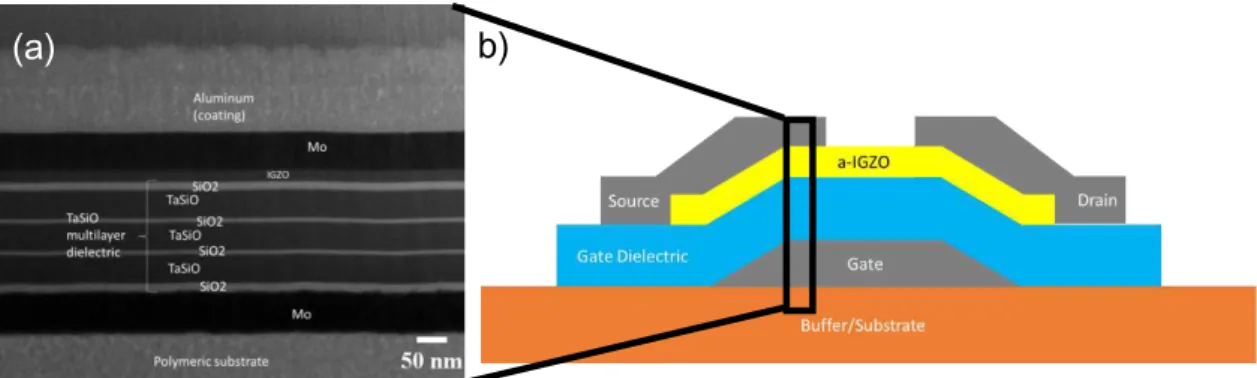
The developed work focuses on the properties of a TFT, meaning the understanding of the multilayer’s composition is of major importance. Also, the interface between the surface can be an indicator of the adhesion between the different layers. A bad adhesion between the layers can diminish the reliability of the system. However, as seen in the TEM Figure 4-1, the layers appear to have a good interface, with overall uniformity.
Figure 4-1: Multilayer System of the TFT: (a) TEM image; (b) schematic of the cross-section of the TFT.
The compositional characterisation of each layer was done using TEM EDS, also obtaining the graphs of Figure C-1, from Appendix C. The graphs show all the layers that compose the TFT and were necessary for the label of each layer, on Figure 4-1. However, a peak of copper is aparent in all the deposited layers, due to the support used for handling the sample.
Since the TFTs are annealed 180 °C for 1 hour, to achieve a better performance, the influence of the temperature on the multilayer system was studied.
(a)
(b)
(
b)
(a)
Mo
Mo
IGZO
12 Influence of uniaxial bending on IGZO TFTs: A study of materials and device
4.1.1
Coefficient of Thermal Expansion (CTE)
Since TEM images do not show any cracks due to thermal annealing of the sample, the stress due to the mismatch between the different CTEs gathered in the layers was not relieved [55]. The molybdenum studied is a pure polycrystalline material when sputtered, and so an in-situ X-ray diffraction at different temperatures was performed on the Mo layer.
40.0 40.5 41.0
0 20000 40000 60000 80000 100000 In te n si ty (co n st a n ts) ( )
Temperature (o
C) 30 50 60 70 80 90 100 110 120 130 140 150 160 170 180 190 200 (110)
(200C) = 40.447
(30C) = 40.481
During Annealing
Figure 4-3: In-situ XRD of molybdenum under heating from 30 °C to 200 °C.
The Mo layer during the annealing dilates as expected. Because of the dilation of the crystal lattice, it is possible to determine the CTE of the molybdenum, according to Equation 7.
(7)
Considering the 2θ values shown in the graph from Figure 4-3, that ΔT = 170 °C, λCu=1.516 Å, and that the crystallographic plane is (110), the determined CTE of the Molybdenum is α = 4.7 ppm/°C, as predicted by the literature [56]. The in-situ DRX was made using only molybdenum, since it is a polycrystalline material, with a very defined peak. Table 4-1 shows the different CTE values for each layer.
Table 4-1: Coefficient of thermal expansion of the different layers in the TFT multilayer structure.
Material CTE (10-6/°C) material CTE (ppm/°C)
PEN [57] 20.0 SiO2 [58] 0.7
PDMS [59] 301.0 Ta2O5 [60] 3.0
Kapton [61] 20.0 IGZO [62] 5.2
molybdenum 4.7 Parylene [63] 35.0
Although mechanical properties, such as hardness and Young modulus, change for thin films, the intrinsic characteristic of this layer behaves as expected. The obtained value of CTE for the
molybdenum is one of the most important factors in choosing this material as an electrode in transistors [64].
4.2
Mechanical Properties of Individual Layers
For a better understanding of mechanical properties of thin films layers of Mo and IGZO, nanoindentation was performed. These measurements were not done on the dielectric layers, given the very high deposition time needed to reach the necessary 400 nm. However, SiO2 layers have been thoroughly studied in other works.
4.2.1
Molybdenum and IGZO Layers
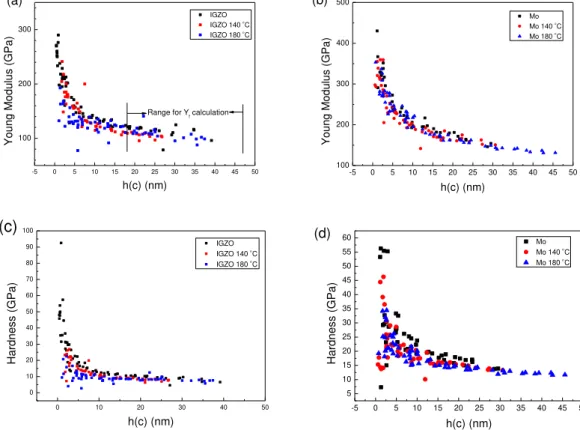
For a better mechanical reliability of the system, it is important to determine mechanical properties of the individual layers of IGZO and Molybdenum, like Young modulus and hardness. Figure 4-4 shows the graphs obtained from the nanoindentation done on the IGZO and molybdenum layers. Since the layers in this study where 400 nm, various indentations where performed in the layer, until a penetration depth of 40 nm, correpondent to 10 % of the thickness of the layer, was achieved.
-5 0 5 10 15 20 25 30 35 40 45 50
100 200 300
IGZO
IGZO 140 C
IGZO 180 C
Youn g Modu lus (GPa) h(c) (nm) (a)
Range for Yf calculation
-5 0 5 10 15 20 25 30 35 40 45 50
100 200 300 400 500 Mo
Mo 140 C
Mo 180 C
Y oun g M odu lus (G P a) h(c) (nm) (b)
0 10 20 30 40 50
0 10 20 30 40 50 60 70 80 90 100 IGZO
IGZO 140 C
IGZO 180 C
Hardnes s (G P a) h(c) (nm) (c)
-5 0 5 10 15 20 25 30 35 40 45 50 5 10 15 20 25 30 35 40 45 50 55
60 Mo
Mo 140 C
Mo 180 C
14 Influence of uniaxial bending on IGZO TFTs: A study of materials and device Table 4-2: Young Modulus and Hardness obtained with nanoindentation in 400 nm thick IGZO and Molybdenum Layers, as deposited, annealed 1 hour at 140 °C and annealed 1 hour at 180 °C.
Young Modulus (GPa) Hardness (GPa)
IGZO
As deposited 116.5 ± 6.9 9.5 ±1.3
140 °C 112.6 ± 23.2 9.0 ± 2.9
180 °C 111.3 ± 11.8 8.3 ± 1.2
Molybdenum
As deposited 171.0 ± 12.4 16.6 ± 1.6
140 °C 167.1 ± 10.4 15.2 ± 1.6
180 °C 159.8 ± 14.7 13.3 ± 1.2
The values for the layers’ mechanical properties, before and after annealing, are slightly different, as observed in Table 4-2, showing a decrease in both Young modulus and hardness, with a bigger difference in the Molybdenum layer. Nevertheless, the values obtained for before and after annealing are in the interval obtained from the standard. The measured value obtained through nanoindentation of the Mo layer shows a considerable difference from the bulk value of 329 GPa [64], observed in literature, which is explained by the very low thickness of the studied layer. For very thin layers, the mechanical properties are dependent on surface factors, unlike what happens in bulk specimens. Nonetheless, since a lower Young modulus is preferred for better bendability of a system, this difference in values is desired.
However, after performing an XRD-diffraction from the same sample as deposited and after annealing at 180 °C for 1 hour, as shown in Figure 4-5, the crystal lattice does not return to the original state, which can also explain the decrease in Young modulus and hardness values after annealing. From the XRD-diffraction it is possible to obtain the crystallites’ size, for each sample, before and after annealing, through the Scherrer equation [65]. The obtained values were 27.39 nm and 28.36 nm for the as-deposited and annealed sample, respectively. The increase in crystallites’ size in the annealed samples explains the decrease in Hardness of the films. According to the Hall-Petch relationship, the decrease in particle size increases the Hardness, as obtained by the nanoindentation measurements [66].
37 38 39 40 41 42 43
100 1k 10k
Mo as deposited Mo 1h@180
Int ensit y (c oun ts )
2 ()
contraction
4.2.2
Parylene Layer
Annealing of the parylene layer dramatically changes the mechanical behaviour, which is expected, since it is a semicrystalline material. During the wedge indentation, the indent is scanned, as seen by the change in indent in Figure 4-6. In the non-annealed sample, the layer is very conformal, while in the annealed one the parylene becomes more rigid. According to Equation 4, it may be possible to work with this property to have a more reliable device.
Figure 4-6: Wedge indent on multilayer with 1 m parylene passivation (a) as deposited; (b) annealed at 180 ºC.
4.3
Flexible Transistors
The thickness of the substrate is one of the main properties that influences the bending of the samples. In the beginning of this work a PEN foil was used, with a thickness of 125 μm. PEN is a transparent polymer, has a very uniform surface, and a transition temperature of 155 ºC [67]. However, because of the high thickness, the substrate is not able to support bending radius of less than 2.5 mm, as seen in Figure 4-7.
Figure 4-7: Optical microscope Images of Mo on PEN: (a) 10 cycles with bending radius of 2.5 mm; (b) 1 cycles with bending radius of 1.25 mm.
The substrate with a bending radius of 1.25 mm has plastic deformation (1 cycle), fracturing the top Mo layer. Since one of the goals is to be able to get the smallest bending radius possible, smaller thickness substrates were used. Kapton (polyimide) is a very thermally stable substrate (Tg > 300 °C), has lower CTE than other polymers, and can be purchased in smaller thicknesses, down to 25 μm. From here on, the 75 μm thick Kapton is referred as K75, 50 μm thick as K50, and 25 μm thick as K25.
500 μm 500 μm
(a)
(b)
16 Influence of uniaxial bending on IGZO TFTs: A study of materials and device
0 1 2 3 4 5
0.0 0.1 0.2 0.3 0.4 f
(Mo
)
Radius (mm) K25 K50 K75 PEN Q51At r=1.25 cm
f(PEN) = 0.0515
f(K75) = 0.033 f(K50) = 0.023
f(K25) = 0.0126
Figure 4-8: Strain on top of Mo depending on the bending radii: in black is K25, in red is K50, in blue is K75, and in pink is PEN with 125 μm.
PEN could not bend for the smaller radius, since the high values of thickness and Young modulus make it so that the strain on the top Mo layer is much higher than on the Kapton substrates, resulting in plastic deformation of the PEN substrate and, subsequently, causing the molybdenum to crack.
4.3.1
Kapton as a Substrate
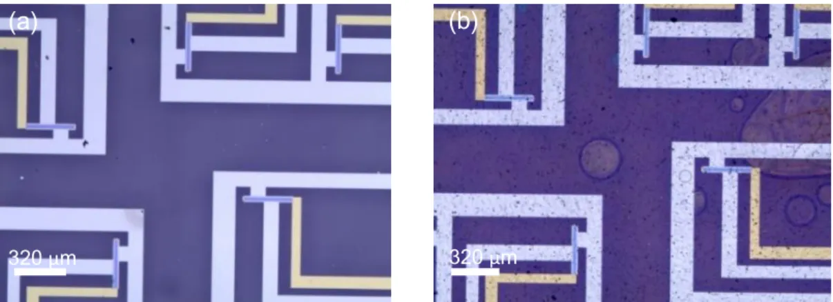
The Kapton used as substrate is a commercially available polymer. The calculations requiring its properties relied on the datasheet [61]. However, characteristics like the roughness of the Kapton were measured using the profilometer, since its surface, shown on the optical microscope in Figure 4-9, was not smooth.
Figure 4-9: Optical microscope image of the TFTs fabricated on (a) glass substrate; (b) Kapton substrate.
As seen in the 3D measurements from Figure E-1, Figure E-2 and Figure E-3 (representative of the sample K75, K50 and K25, respectively), the surface is not totally flat, presenting peaks throughout the surface. From these 3D maps, it was possible to determine the average roughness of the substrate, which is presented in Table 4-3, for the several thicknesses.
(a)
(b)
Table 4-3: Roughness values for samples K75, K50 and K25.
K75 K50 K25
Average Roughnes (nm) 58 67 105
RMS Roughnes (nm) 95 94 128
Peak to Valley Heigh (nm) 2379 1388 1810
The obtained root mean squase (RMS) roughness is not the most ideal, especially on the thinnest substrate. However, this value is probably higher than the real one, due to the substrates’ flexible nature. During the measurement, the substrates were not totally flat, meaning this could increase the measured roughness. For example, the 3D map of the K25 substrate, Figure E-3,in appendix E, shows with high probability the previous situation, since one of the corners is purple. Also, since transistors’ dimensions of width and length are in the order of magnitude of micrometers, substrate’s roughness creates pinholes that could possibly affect TFTs properties.
4.3.2
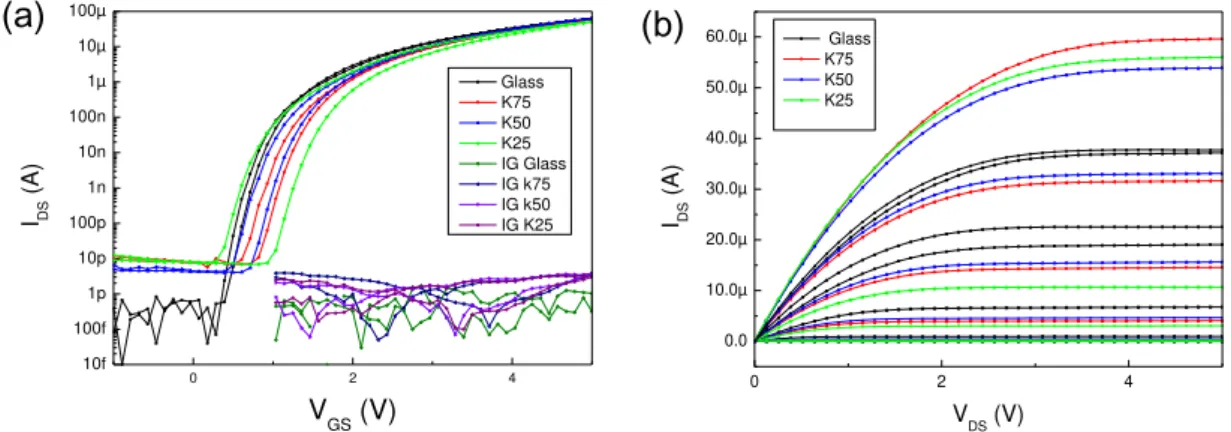
IGZO TFTs
To study the electrical properties of TFTs on the different substrates, and to characterise the influence of bending on the transistors, the characteristic curves of TFTs were determined. From them, the parameters of TFTs, such as the Ion/Ioff ratio, Von, leakage current (IG), hysteresis, mobilitiy (μsat) and threshold voltage (VT) were obtained.
18 Influence of uniaxial bending on IGZO TFTs: A study of materials and device
0 2 4
10f 100f 1p 10p 100p 1n 10n 100n 1µ 10µ 100µ IDS (A)
VGS (V)
Glass K75 K50 K25 IG Glass IG k75 IG k50 IG K25
0 2 4
0.0 10.0µ 20.0µ 30.0µ 40.0µ 50.0µ 60.0µ IDS (A)
VDS (V) Glass
K75 K50 K25
Figure 4-11: Characteristic curves of TFTs fabricated in Glass substrate (black), K75 (red), K50 (blue), and K25 (green): (a) Transfer characteristic curve, where the IG starts at 1 V for ease of
comprehension of the graph, and (b) Output characteristic curve.
Table 4-4 summarizes the results for the parameters of the transistors in the different substrates. Comparing the results, it is possible to see that the Ion/Ioff of the glass substrate transistors is more than an order of magnitude higher than the Kapton ones, due to the higher surface roughness of the Kapton substrates. The Ion/Ioff is very similar between the Kapton substrate transistors. The leakage current increases with the decrease in thickness of the substrate. Nonetheless, it is still a very low value. The mobility of the transistors is around 6 cm2V-1s-1, which is a lower value than the usually published ones in the literature, due to the IGZO used. The IGZO has the composition of 1:1:1 molar ratio, presenting less concentration of indium than other IGZO compositions, which is known to decrease the mobility [69].
Table 4-4: Summary of IGZO TFTs parameters, in glass and polymer substrates.
Glass K75 K50 K25
Ion/Ioff (2.3 ± 4.3) ×108 (7.7 ± 3.2) ×106 (11 ± 5.9) ×106 (7.4 ± 5.2) ×106
Von (V) 0.30 ± 0.15 0.51 ± 0.08 0.27 ± 0.23 0.26 ± 0.19
IG (pA) 2.1 ± 1.3 5.6 ± 3.9 35.0 ± 70.0 57.0 ± 120.0
Hysteresis (V) 0.12 ± 0.06 0.15 ± 0.06 0.46 ± 0.15 0.33 ± 0.00
μsat (cm2V-1s-1) 5.9 ± 1.7 6.6 ± 0.3 6.3 ± 0.5 5.5 ± 0.6
VT (V) 2.95 ± 0.10 3.12 ± 0.06 2.97 ± 0.15 2.97 ± 0.10
Nonetheless, the transistors on Kapton substrates still have very good performances and are suitable for bending tests.
4.3.3
Iddle shelf Time
Since TFTs were fabricated in thick rigid glass substrates, and in flexible thinner substrates, the influence of time on their performance was studied, to understand if the different substrates yield different results with the aging of the devices.
0 2 4 10f 100f 1p 10p 100p 1n 10n 100n 1µ 10µ 100µ IDS (A)
VGS (V)
ID Glass ID Glass (3 weeks) IG Glass IG Glass (3 weeks)
0 2 4
0.0 10.0µ 20.0µ 30.0µ 40.0µ 50.0µ 60.0µ 70.0µ 80.0µ 90.0µ IDS (A) V
DS (V)
ID Glass ID Glass (3 weeks)
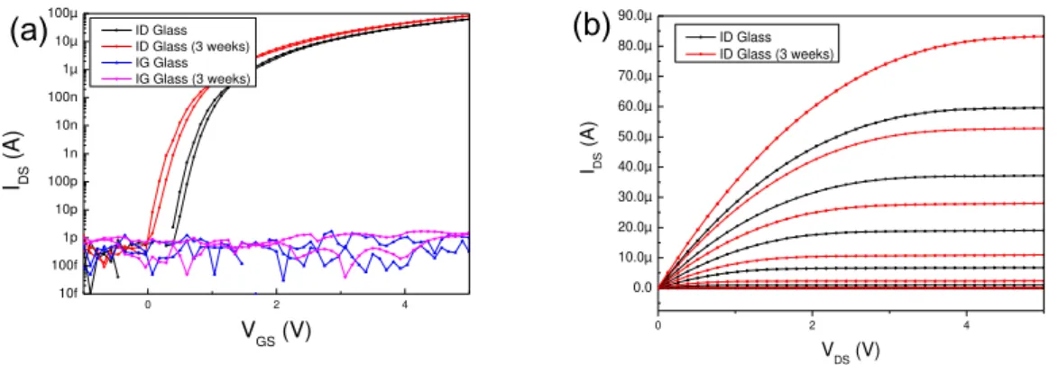
Figure 4-12: Characteristic curves of IGZO TFTs fabricated on corning glass right after production (black), and three weeks after production (red): (a) Transfer characteristic curve, and (b) output characteristic curve.
As seen in Figure 4-12, the transistors fabricated on glass shift to more negative values after three weeks. However, the performance of TFTs regarding Ion/Ioff, IG and mobility, presented in Table 4-5, achieve better values since TFTs were aged in an air-based atmosphere. The IGZO semiconductor becomes more conductive with time, because of the desorption of the oxygen atoms in the metal-oxide-metal lattice [32].
Table 4-5: Summary of IGZO TFTs parameters fabricated on Corning glass after production and after three weeks, in an oxygen rich environment.
Ion/Ioff (108)
Von (V) IG (pA) Hysteresis (V) μsat (cm2V-1s-1)
VT (V)
Glass 2.3 ± 4.3 0.30 ± 0.15 2.1 ± 1.3 0.12 ± 0.06 5.9 ± 1.7 2.95 ± 0.10
Glass
(3 weeks) 6.3 ± 9.4 -0.08 ± 0.18 1.6 ± 0.8 0.11 ± 0.00 6.6 ± 0.3 2.93 ± 0.09
However, unlike what happens with TFTs on a glass substrate, TFTs fabricated on a thin polyimide substrate have an increase in leakage current, that translated in a decrease of Ion/Ioff, visually represented in Figure 4-13. This happens due to the higher gas permeability of the polyimide substrate, and because of the thinner nature of the flexible substrate regarding the glass substrate [12]. Nonetheless, when comparing the transistors regarding Von, hysteresis, mobility and VT, they present the same behaviour as TFTs on corning glass.
20 Influence of uniaxial bending on IGZO TFTs: A study of materials and device
0 2 4
10f 100f 1p 10p 100p 1n 10n 100n 1µ 10µ 100µ IDS (A) V
GS (V)
ID K25 ID K25 (1 month) IG K25 IG K25 (1 month)
0 2 4
-10.0µ 0.0 10.0µ 20.0µ 30.0µ 40.0µ 50.0µ 60.0µ 70.0µ 80.0µ IDS (A)
VDS (V)
ID K25 ID K25 (1 month)
Figure 4-13: Characteristic curves of TFTs fabricated on a kapton substrate (25 μm) after fabrication (black) and after one-month (red): (a) Transfer characteristic curve, and (b) output characteristic curve.
Table 4-6: Summary of IGZO TFTs parameters fabricated on Kapton substrate (25 um), after production and after one month in an oxygenated atmosphere.
Ion/Ioff (106)
Von (V) IG (nA) Hysteresis (V) μsat (cm2V-1s-1)
VT (V)
K25 7.4 ± 5.2 0.26 ± 0.186 574 ± 12.3 0.33 ± 0.00 5.52 ± 0.56 2.97 ± 0.10
K25 (after
1 month) 0.8 ± 0.3 0.01 ± 0.06 4.2 ± 12.3 0.29 ± 0.09 6.26 ± 0.80 2.98 ± 0.08
4.3.4
Peel-Off (Metal Blade)
Since during the fabrication of the transistors, the substrate is glued to the glass, a peel-off process in necessary to have free-standing samples. In this substrate, the peel-off is done mechanically with a metal blade, since the resin used to glue the substrate to the carrier glass does not dissolve without compromising the layers of this samples.
Figure 4-14:Characteristic curves of TFTs fabricated on a K75glued to carrier substrate (black), after delamination (red) and after delamination and annealing (blue): (a) Transfer characteristic curve, and (b) output characteristic curve.
0 2 4
10f 100f 1p 10p 100p 1n 10n 100n 1µ 10µ 100µ IDS (A)
VGS (V)
ID K75 ID K75 Del ID K75 Del RT IG K75 IG K75 Del IG K75 Del RT
0 2 4
0.0 10.0µ 20.0µ 30.0µ 40.0µ 50.0µ 60.0µ IDS (A)
VDS (V)
ID K75 ID K75 Del ID K75 Del RT
(a)
(b)
After the delamination, Von shifted to more positive values and the Ion/Ioff ratio diminished, as seen in Figure 4-14. However, the transistors, with the increase in time and thermal treatment, somewhat recuperated, achieving a better Ion/Ioff and shifting Von to less positive values. After analysing Table 4-7, it is seen that IG increased significantly after the delamination, and that both IG and hysteresis did not recover
Table 4-7: Summary of IGZO TFTs parameters, in the K75 substrate, before delamination, after delamination, and delamination and annealing.
K75 K75 Delaminated K75 Delaminated RT
Ion/Ioff (7.7 ± 3.2) × 106 (3.7 ± 3.4) × 106 (4.3 ± 2.1) × 106
Von (V) 0.51 ± 0.08 1.39 ± 0.40 0.92 ± 0.22
IG (pA) 5.6 ± 4.0 73.7e ± 170 97.4 ± 234.9
Hysteresis (V) 0.15 ± 0.05 0.20 ± 0.04 0.27 ± 0.06
μsat (cm2V-1s-1) 6.6 ± 0.3 5.3 ± 1.5 5.2 ± 0.4
VT (V) 3.12 ± 0.06 3.94 ± 0.33 3.62 ± 0.10
Although the peel-off process is not the most ideal, for 75 μm thick substrates it yields good results.
4.3.5
Bending
The transfer curves presented until now were determined while transistors were in a flat condition. Since this work focuses on the mechanical reliability of transistors under mechanical uniaxial stress, transfer curves of the transistors while under bending were made. The system uses moulds with radii 45, 25 and 15 mm. Giventhe location of the pads and the system in use, smaller radii were not possible to measure. In Appendix F, there are several pictures of the TFT matrix under a bending measurement with radius of 25 mm.
22 Influence of uniaxial bending on IGZO TFTs: A study of materials and device
0 2 4
10f 100f 1p 10p 100p 1n 10n 100n 1µ 10µ 100µ I DS (A)
VGS (V)
ID flat1 ID T45 ID C45 ID flat 2 ID T25 ID C25
0 2 4
10f 100f 1p 10p 100p 1n 10n 100n 1µ 10µ 100µ I DS (A)
VGS (V)
ID flat 1 ID t45 ID c45
Figure 4-16: Characteristic curves of TFTs under bending with radii of 45, 25 and 15 mm: (a) transfer curve for TFTs with channel perpendicular to bending direction; (b) transfer curve for TFTs with channel parallel to bending direction
As it is possible to observe in the graphs of Figure 4-16, the transistors shift positively after each consequent measurement, both for when the channel is perpendicular, Table G-1, or parallel to the bending direction, Table G-2 in Appendix G, having no apparent pattern when the channel is under compression or tension. However, as the radius decreases, the performance of TFTs appears to degrade.
Measurements were made on the TFTs after three days, while flat (flat 3.1 on Table G-1 and G- 2), to see if the TFTs recover. In both occasions, this occurred with an increase in mobility and a negative Von shift, showing that the bending stress is reversible.
However, considering the measurements’ sequence regarding the gradual diminish of bending radius and given the necessity of doing various measurements on the same transistors, TFT’ operation changes could also be explained due to the bias stress, and not because of the decrease in bending radius. To test this hypothesis, measurements of TFTs were done randomly from which the Table 4-8 was obtained and the graphs from Figure H-1 in Appendix H were obtained The positive Von shift does not depend on the bending radius. When diminishing or increasing the radius the positive Von shift always occurs for consequent measurements. So, although the bending radii of 45, 25 and 15 mm does not affect the TFTs behaviour, it is important to consider the inflicted electrical stress. This effect on the transistors can also be observed on the transistors when doing three consecutive measurements when the transistors did not have any mechanical force applied, represented in Figure H-2 from Appendix H.
Table 4-8:Summary of IGZO TFTs, fabricated on the K75 substrate in bending and flat conditions, with radii 45, 25 and 15 mm
Ion/Ioff (× 106)
Von (V)
IG (pA)
Hysteresis (V)
μsat (cm2V-1s-1)
VT (V)
Before
peel-off 18.6 ± 10.8 0.55 ± 0.06 14.7 ± 19.2 0.40 ± 0.08 6.26 ± 1.82 3.14 ± 0.04
After
peel-off 11.0±5.41 1.4 ± 1.1 64.0±90.8 0.425±0.05 7.94 ± 3.22 5.05±2.34
T25 6.2±3.89 0.8±0.14 617±867 0.4±0.0 7.17 ± 3.87 3.84±0.104
flat2 7.13±2.57 1.1±0.57 896±200 0.55±0.07 7.81±2.56 4.85±1.05
T15 16.9±17.6 1.6±0.7 1730±2420 0.5±0.14 8.16±2.22 5.71±1.27
Flat 3 15.1±12.9 1.85±0.49 1450±1990 0.6±0.14 8.53±2.79 6.43±1.22
C25 19.3±17.6 2.15±0.21 1730±2390 0.6±0.1 9.34±2.45 6.72±1.09
Flat 4 47.4±49.5 2.25±0.35 3190±4430 0.75±0.07 10.6±0.7 7.61±1.04
C45 58.4±69.7 2.75±0.21 3080±4280 0.9±0.28 11.3±1.79 8.45±0.28
4.3.6
Substrate Peel-off
The peel-off process is very dependent on the user. Although the K75 sample could still yield functioning transistors, some part of the sample cracked, which made the measurements on the pads of some transistors not possible, as seen in Figure I-1, from Appendix I.
Although the K75 delaminated without cracking most of the sample, the same did not happen with the K50 and K25 samples. The peel-off is done with a metal blade, and, even if this type of delamination works well for thicker substrates, the thinner substrates could not withstand this process and cracked, which is represented in Figure I-2, from Appendix I.
24 Influence of uniaxial bending on IGZO TFTs: A study of materials and device Figure 4-17: SEM images of the K25 delaminated sample: (a) surface with the SE2 detector, (b)
cross-section of crack in TFT.
Analysing the SEM images, it is possible to see that the substrate cracks where the dielectric is in contact with the substrate. However, the bottom molybdenum (gate contact) can withstand the process. This means that, although the substrate cracks, these cracks do not propagate through the bottom contact, which results on the multilayer to remain reliable. To test this, measurements were done of the transfer curves of the transistors, with the microprobe on the transistors (and not on the pads), as schemed in Figure I-3, from appendix I.
0 2 4 6
100f 1p 10p 100p 1n 10n 100n 1µ 10µ 100µ IDS (A)
VGS (V)
ID (before delamination) ID (after delamination) IG (before delamination) IG (after delamination)
0 2 4 6
0.0 10.0µ 20.0µ 30.0µ 40.0µ 50.0µ 60.0µ 70.0µ 80.0µ IDS (A)
VDS (V) ID (before delamination) ID (after delamination)
Figure 4-18: Characteristic curves of a TFT in the K25 sample before and after delamination, with probes on TFTs: (a) Transfer curve; (b) Output characteristic curve.
It is then possible to affirm that, although the peel-off process cracks the dielectric multilayer and substrate, it is generally not enough for the transistor (on top of the gate electrode) to stop working. The main consequence of this would be that, although the transistors would still be intact, the circuit would not be able to propagate the signal and no current would be possible to obtain from the drain to the source (IDS).
Gate Drain
Source
Substrate
Channel Dielectric
100 μm 1 μm
![Figure 1-1: Market Forecast for Asia Pacific Flexible Electronics Market by Application (Consumer Electronics, Automotive, Healthcare, Industrial) (USD Million) until 2024 [3]](https://thumb-eu.123doks.com/thumbv2/123dok_br/16693496.743730/25.892.234.703.318.581/forecast-flexible-electronics-application-electronics-automotive-healthcare-industrial.webp)
![Figure 2-5: Examples of state of the art methods for better TFT flexibility: (a) double gate TFT structures [42]; (b) nanowires [43]; (c) mesh and strip pattering layers [44]](https://thumb-eu.123doks.com/thumbv2/123dok_br/16693496.743730/30.892.125.779.309.466/figure-examples-methods-better-flexibility-structures-nanowires-pattering.webp)