João Carlos Ferreira de Almeida Casaleiro
LicenciadoAnalysis and Design of Sinusoidal Quadrature
RC-Oscillators
Dissertação para obtenção do Grau de Doutor em
Engenharia Electrotécnica e de Computadores
Orientador: Luís Augusto Bica Gomes de Oliveira, Professor Auxiliar, Universidade Nova de Lisboa
Júri
Presidente: Prof. Dr. Paulo da Costa Luís da Fonseca Pinto Arguentes: Prof. Dr. João Manuel Torres Caldinhas Simões Vaz
Prof. Dr. Vítor Manuel Grade Tavares Vogais: Prof. Dr. Igor Filanovsky
Prof. Dr. Jorge Manuel dos Santos Ribeiro Fernandes Prof. Dr. Luís Humberto Viseu Melo
Analysis and Design of Sinusoidal Quadrature RC-Oscillators
Copyright © João Carlos Ferreira de Almeida Casaleiro, Faculdade de Ciências e Tecnologia, Universidade NOVA de Lisboa.
A
C K N O W L E D G E M E N T S
I would like to express my sincere thanks to my supervisor Prof. Dr. Luís Augusto Bica Gomes de Oliveira for the continuous support, for his patience and motivation. His supervision helped me focus on the research and writing of this thesis. Besides my supervisor, I would like to thank Prof. Dr. Igor M. Filanovsky for his long lessons on differential equations and on Van der Pol oscillators, which were essential for the research, and for his suggestions to clarify the text.
Further, I would like to thank the other members of my thesis committee: Prof. Dr. João Goes and Prof. Dr. Manuel Medeiros Silva for their suggestions to focus the research. I wish to present my special thanks to Prof. Dr. Manuel Medeiros Silva for the contribution to the thesis’s quality, for the helpful discussions about the capacitive coupling theory, and his illuminating suggestions to clarify the text. In addition, I thank my fellow lab mates in UNINOVA for the support with the simulations and the stimulating discussions. Also, I thank my friends in CEDET for the overall support and encouragement.
I acknowledge the support given by the following institutions:
• Instituto Superior de Engenharia de Lisboa – ISEL, for the 6-month sabbatical leave for the writing of this thesis.
• Portuguese Foundation for Science and Technology (FCT/MCTES) (CTS multi-annual funding) through PIDDAC program funds and under projects DISRUPTIVE (EXCL/EEI-ELC/0261/2012) and PEST (PEST-OEEEI/UI0066/2014), for the financial support.
A
B S T R A C T
integrator oscillator study, it was found that the quadrature error can be eliminated by adjusting the transconductances to compensate the capacitance mismatch. However, to obtain outputs in perfect quadrature one must allow some amplitude error.
R
E S U M O
simulações mostraram que o ruído de fase diminui com o aumento do fator de acoplamento. Assim sendo, não existe compromisso entre o erro de quadratura e o ruído de fase do oscilador. A teoria do oscilador com dois integradores revelou que o erro de quadratura pode ser eliminado, ajustando as transcondutâncias de forma a compensarem a assimetria das capacidades. No entanto, para obter saídas em perfeita quadratura tem de existir alguma diferença nas amplitudes.
C
O N T E N T S
List of Figures xv
List of Tables xix
1 Introduction 1
1.1 Background and motivation . . . 1
1.1.1 Quadrature signal generation . . . 2
1.2 Organization of the thesis . . . 6
1.3 Main contributions . . . 7
2 Sinusoidal oscillators 9 2.1 Introduction . . . 9
2.2 Sinusoidal oscillator models . . . 9
2.3 Amplitude control . . . 15
2.3.1 Equilibrium points and stability . . . 16
2.3.2 Negative-resistance circuits . . . 20
2.4 Frequency selectivity . . . 22
3 Injection Locking 27 3.1 Introduction . . . 27
3.2 Parallel VDPO . . . 29
3.3 Series VDPO . . . 34
3.3.1 Single external source . . . 35
3.3.2 Double external source . . . 37
3.4 Conclusion . . . 38
4 Active couplingRC−oscillator 39 4.1 Introduction . . . 39
4.2 SingleRC−oscillator . . . 40
4.2.1 Start-up conditions . . . 43
4.2.2 Quality factor . . . 44
4.2.3 Design and simulation result . . . 45
4.3.1 Incremental model . . . 47
4.3.2 Quadrature oscillator without mismatches . . . 49
4.3.3 Stability of the equilibrium points . . . 50
4.3.4 Quadrature oscillator with mismatches . . . 52
4.4 Simulation results . . . 54
4.5 Conclusions . . . 56
5 Capacitive couplingRC−oscillator 59 5.1 Introduction . . . 59
5.2 Quadrature oscillator . . . 61
5.2.1 Two-port modelling of capacitive coupling networks . . . 61
5.2.2 Incremental model . . . 64
5.2.3 Oscillators without mismatches . . . 67
5.2.4 Stability of the equilibrium points . . . 69
5.2.5 Mode selection . . . 74
5.2.6 Capacitive coupling oscillator with mismatches . . . 74
5.3 Experimental results . . . 83
5.4 Conclusion . . . 87
6 Two-integrator oscillator 89 6.1 Introduction . . . 89
6.2 Quadrature oscillator . . . 91
6.2.1 Transconductance amplifier . . . 91
6.2.2 Negative resistance circuit . . . 93
6.2.3 Incremental model . . . 94
6.2.4 Oscillator without mismatches . . . 95
6.2.5 Stability of the equilibrium points . . . 97
6.2.6 Oscillator with mismatches . . . 98
6.3 Simulation results . . . 102
6.4 Conclusions . . . 105
7 Conclusions and future research 107 7.1 Conclusions . . . 107
7.2 Future research . . . 109
Appendix A The MOSFET transconductance with weak nonlinearity 111 A.1 Strong inversion . . . 111
A.2 Weak inversion . . . 113
Appendix B Reducing VDP homogeneous equation to the first order 115
C O N T E N T S
Appendix D Impact of the mismatches in the capacitive coupled oscillator 123 D.1 Oscillation frequency . . . 123 D.2 Amplitude error . . . 126 D.3 Phase error . . . 129
L
I S T O F
F
I G U R E S
Fig. 1.1 Low-IF receiver front-end block diagram. . . 2
Fig. 1.2 Direct upconversion transmitter block diagram. . . 2
Fig. 1.3 RC-CRnetwork circuit . . . 3
Fig. 1.4 PassiveRCpolyphase filter with n stages. . . 3
Fig. 1.5 Digital divider-by-two (a) circuit, (b) waveforms, and (c) waveforms with phase error. . . 4
Fig. 2.1 Oscillator feedback model. . . 10
Fig. 2.2 Oscillator negative-resistance model. . . 11
Fig. 2.3 ParallelLC−oscillator. . . 12
Fig. 2.4 ParallelLC−oscillator rearranged in a feedback model. . . 12
Fig. 2.5 Root locus. . . 13
Fig. 2.6 Time solutions for amplitude (a) decay, (b) steady, and (c) growth. . . 13
Fig. 2.7 Negative-resistance model of (a) parallel, (b) seriesLC−oscillator. . . 14
Fig. 2.8 Conceptually automatic amplitude control. . . 15
Fig. 2.9 Parallel Van der Pol oscillator. . . 16
Fig. 2.10 Van der Pol oscillator (a) phase diagram, (b) time-domain solution. . . 18
Fig. 2.11 Amplitude curve of the Van der Pol oscillator. . . 19
Fig. 2.12 Negative resistance circuit. . . 20
Fig. 2.13 Negative resistance small-signal equivalent circuit. . . 21
Fig. 2.14 Negative resistance circuit (a) and the small-signal equivalent (b). . . 22
Fig. 2.15 Loop gain frequency response. . . 24
Fig. 3.1 Beat. . . 28
Fig. 3.2 Injection-lock parallel VDPO . . . 29
Fig. 3.3 Phase curve of the injection-lock parallel VDPO (a) and the time solution of path path P (b). . . 31
Fig. 3.4 Injection Lock phase curve. . . 32
Fig. 3.5 Amplitude phase curve of the injection locking . . . 33
Fig. 3.6 Amplitude as a function of the oscillation frequency. . . 34
Fig. 3.7 Driven series Van der Pol oscillator. . . 35
Fig. 3.8 Phase curve of the series VDPO. . . 36
Fig. 3.10 Driven series Van der Pol oscillator with double injection. . . 37
Fig. 4.1 SingleRC−oscillator (a) circuit and (b) small-signal equivalent circuit. . . 40
Fig. 4.2 Equivalent circuit of a singleRC−oscillator. . . 41
Fig. 4.3 Oscillation (a) amplitude and (b) frequency. . . 45
Fig. 4.4 Quadrature oscillator with active coupling. . . 47
Fig. 4.5 Active coupling small-signal equivalent circuit. . . 48
Fig. 4.6 Series active coupling. . . 52
Fig. 4.7 Impact of the resistance and capacitances mismatches on the amplitude error, using the circuit parameters: R=210Ω, I =600 µA, andIcp=100 µA(α= gm0≈0.758mS). . . 55
Fig. 4.8 Impact of the resistance and capacitances mismatches on the phase error, using the circuit parameters:R=210Ω,I=600 µA, andIcp=100 µA(α=gm0≈0.758 mS). . . 55
Fig. 4.9 Phase error as a function of the coupling strength, using the circuit parameters: R=210Ω,I=600 µA. . . 56
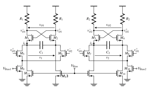
Fig. 5.1 Quadrature oscillator with capacitive coupling circuit. . . 60
Fig. 5.2 Capacitive network currents. . . 61
Fig. 5.3 Incremental circuit of a singleRC−oscillator (a) and simplified circuit (b). . . . 62
Fig. 5.4 Coupling with two-port networks. . . 63
Fig. 5.5 Coupled VDPOs. . . 64
Fig. 5.6 Phase space of the capacitive coupling oscillator. . . 71
Fig. 5.7 Capacitive coupling (a) phase-portrait and (b) transient for path
P
. . . 72Fig. 5.8 Oscillation frequency of the capacitive coupling. . . 77
Fig. 5.9 Simulation results for the amplitude error of the capacitive coupling. . . 79
Fig. 5.10 Simulated phase error. . . 83
Fig. 5.11 Phase noise and phase error. . . 83
Fig. 5.12 Prototype circuit of the capacitive coupling oscillator. . . 84
Fig. 5.13 3-bit binary weighted capacitor array (a), photo of the daughterboard (b), the microphotos of the capacitive coupling QVCOs with capacitor array (c), and without capacitor array (d). . . 85
Fig. 5.14 Frequency of oscillation with the oscillators uncoupled and coupled (CX=20fF). 85 Fig. 5.15 Relation between the oscillation frequency and the coupling strength. . . 86
Fig. 5.16 Measured phase noise. . . 86
Fig. 6.1 Conceptual model of the two integrator oscillator. . . 90
Fig. 6.2 Two integrator oscillator. . . 91
LI S T O F FI G U R E S
Fig. 6.5 Negative resistance circuit. . . 93
Fig. 6.6 Negative resistance equivalent circuit. . . 94
Fig. 6.7 Two integrator small-signal equivalent circuit model. . . 95
Fig. 6.8 Impact of the resistance mismatches on the amplitude error. . . 102
Fig. 6.9 Phase error as function of transconductance. . . 103
L
I S T O F
T
A B L E S
5.1 Comparison of state-of-the-art nearly sinusoidalRC−Oscillators with the same circuit topology. . . 87
A
C R O N Y M S
AAC Automatic amplitude control
CMOS Complementary metal-oxide-semiconductor FoM Figure-of-merit
ILFD Injection-locked frequency divider IoT Internet-of-things
IRR Image rejection ratio
ISM Industrial, scientific and medical KCL Kirchhoff’s current law
KVL Kirchhoff’s voltage law MIMO Multi-input multi-output
MOSFET Metal-oxide-semiconductor field effect transistor OFDM Orthogonal frequency division multiplexing QAM Quadrature amplitude modulation
QO Quadrature oscillator
QPSK Quadrature phase-shift keying
QVCO Quadrature voltage-controlled oscillator RF Radio frequency
SNR Signal-to-noise ratio THD Total harmonic distortion VDP Van der Pol
VDPO Van der Pol oscillator
C
H
A
P
T
E
R
1
I
N T R O D U C T I O N
Contents
1.1 Background and motivation . . . 1 1.1.1 Quadrature signal generation . . . 2 1.2 Organization of the thesis . . . 6 1.3 Main contributions . . . 7
1.1
Background and motivation
The objective of an oscillator circuit is to generate a periodic signal. Radio frequency circuits require sinusoidal oscillators (or second-order oscillators) with a stable amplitude, frequency and phase. Digital circuits and analog-to-digital converters require square-wave signals, known as clock signal. These signals are generated by relaxation oscillators (also called first-order oscillators), a topic that is outside the scope of this thesis and will not be further discussed. In this thesis, the investigation is focused on sinusoidal oscillators.
LNA
LO1 I
Q LO2
Q I
+
+-+
+ +BB I
BB Q LNA- Low Noise Amplifier
LO- Local quadrature oscillador BB- Base band
Figure 1.1: Low-IF receiver front-end block diagram.
BB I
BB Q
LO I
Q
+
+
-PA
BB- Base Band
LO- Local quadrature oscillator PA- Power Amplifier
Figure 1.2: Direct upconversion transmitter block diagram.
of applications, such as wireless sensor network (WSN), home automation, healthcare, smart energy, and many others. Moreover, in modern receivers the cost and size reduction are important requirements. The minimization of external components reduces the equipment cost. Full integration poses several challenges. For instance, the Low-IF receiver requires image cancellation. If quadrature signals are available, the image-rejection filters requiring a large die area can be avoided [1, 3].
Modern RF transmitters, like the direct upconversion shown in Fig. 1.2, using spectrum efficient modulations, such as orthogonal frequency division multiplexing (OFDM) also require QO with accurate quadrature signals. The quadrature error can limit the achievable signal-to-noise ratio (SNR) at the receiver and the size of supported constellation and data rates. Currently, signal processing techniques in the digital domain are used to compensate the quadrature error [4].
1.1.1 Quadrature signal generation
1 . 1 B AC K G RO U N D A N D M OT I VAT I O N
Vin
C R
VI
R
C VQ
Figure 1.3:RC-CRnetwork circuit
Vin−
Vin
Vin+
R1
C1
R1
C1
R1
C1
R1
C1
R2
C2
R2
C2
R2
C2
R2
C2
Rn
Cn
Rn
Cn
Rn
Cn
Rn
Cn
Io+
Qo+
Io−
Qo−
Figure 1.4: PassiveRCpolyphase filter with n stages.
1.1.1.1 RC-CRnetwork
This method splits the input signalVin in two, passing it in theRCandCRbranches, as shown
Fig. 1.3. TheCRbranch is a high-pass filter that shifts the signal by -45 ° and theRCbranch is a low-pass filter that shifts the signal by +45 °, at the pole frequencyωp≈1/(RC). Although, the
Master D D
Q Q
CLK
Slave D D
Q Q
CLK
vin
vI vQ
(a)
v
inv
Iv
Qt
(b)
v
inv
Iv
Qt
Error(c)
Figure 1.5: Digital divider-by-two (a) circuit, (b) waveforms, and (c) waveforms with phase error.
between them. Hence, in practical circuit there are amplitude- and quadrature-errors. To minimise the errors more stages can be added to the network, as shown in Fig. 1.4. A multi-stageRC−CR network is known as a polyphase filter. With more stages, the errors decrease and the operating bandwidth increases, but the signal loss increases considerably.
1.1.1.2 Frequency division
Frequency dividers are wideband quadrature generators. However, the divider-by-two method uses twice the nominal frequency which increases the power requirements, especially at high frequencies [2]. The divider consists of two latches connected in a master/slave configuration, as shown in Fig. 1.5(a). A square-wave input signal with 50% duty-cycle is required to generate two quadrature signals, as shown in Fig. 1.5(b). If the input signal does not have a 50% duty-cycle, then the output signals have a quadrature error, as shown in Fig. 1.5(c). This problem can be solved by using a divider-by-four, but in this case the frequency of the input signal must be four times the desired operating frequency.
The divider-by-two based on latches is inadequate for quadrature sinusoidal signals because the outputs are square-waves. Hence, it requires additional filtering that needs a large chip area to cope with the components mismatches. For sinusoidal outputs dynamic frequency dividers, such as the injection-locked frequency divider (ILFD) [5, 6] or the regenerative divider [7, 8], are more adequate.
1 . 1 B AC K G RO U N D A N D M OT I VAT I O N
1.1.1.3 Coupled oscillators
The closed-loop approaches, include coupled oscillators and ring oscillators. The best are the QOs based on two coupledLC−oscillators: they have the lowest phase-noise and phase error [9]. Recently it was also shown that they can achieve perfect quadrature [10]. However, coupled LC−oscillators require two inductors, which, depending on the frequency, can occupy a large die area. Moreover, inductors do not scale down with the technology, and designing inductors with acceptable quality factor (Q>5) requires the use of thick top metal layers, increasing the chip cost [11]. Inductorless oscillators, like the two-integrator oscillator or the coupledRC-oscillators, are viable alternatives to avoid the use of inductors. Although, in comparison with the coupled LC−oscillators both have poor phase-noise performance [9], for industrial, scientific and medical (ISM) band, the phase-noise of inductorless oscillators may satisfy the requirements. For instance, the phase-noise specification for 2.4-GHz ISM band at the offset of 1 MHz from the carrier is -110 dBc/Hz for Bluetooth and -88 dBc/Hz for Zigbee; these values are within the performance
capability of inductorless oscillators [12].
The analysis of sinusoidal oscillators using the linear positive feedback model usually is sufficient for deriving the oscillation frequency. However, due to the circuit linearization, as will be shown below, the amplitude limiter mechanism is lost, since it is dependent of the circuit nonlinearities. A large-signal analysis can overcome this limitation, but leads to long and complicated equations that do not help the designer. In this thesis an analysis, based on the weak nonlinearity of the transistors’ transconductances, is presented. This approach allows to avoid a large-signal analysis.
Coupled oscillators consist of two identical oscillators connected by either an active or a passive network. Several active coupling methods were proposed; they can be grouped into parallel or series topologies. The parallel topology was first proposed in [13] forLC−oscillators, with the coupling amplifier transistors in parallel with the oscillators’ core. In the series topology, proposed in [14], the transistors are in series with the oscillators’ core. A comprehensive comparison between these two topologies forLC−oscillators can be found in [15]. The disadvantage of the parallel topologies is the use of two extra gain blocks, which increases the power dissipation [2]. The series topology reuses the current of the oscillator, but the output swing is limited. Since the trend in future complementary metal-oxide-semiconductor (CMOS) technologies is to lower the supply voltages towards 0.5-0.7V [16], this topology is not useful for future designs.
In passive coupling, the amplifiers are substituted by passive elements (usually inductors or capacitors). The coupling based on inductors [17] and transformers [18, 19], requires a higher area than active coupling. Capacitive coupling ofLC−oscillators has shown interesting results [20]; as opposed to traditional active coupling, it does not increase the power consumption. However, the area minimization is still limited by the inductors and the oscillation frequency is lower [21].
capacitors do not add noise, we expect a 3 dB phase-noise improvement (due to the coupling), and with a marginal increase of the power, a figure-of-merit (FoM) comparable to that of the best state-of-the-artRC−oscillators is achieved. Contrarily to what might be expected, with the increase of the coupling capacitances (higher coupling strength) the oscillation frequency increases [22]. We present the theory to explain this behaviour, and we derive the equations for the frequency, phase-error and amplitude mismatch, which are validated by simulation. The theory shows that the phase-error is proportional to the amplitude mismatch, indicating that an automatic phase-error minimization based on the amplitude mismatch is possible. We also study bimodal oscillations and phase ambiguity, for this coupling topology, comparing it with other circuits [23]. To validate the theory, a 2.4-GHzquadrature voltage-controlled oscillator (QVCO) based on twoRC−oscillators with capacitive coupling was fabricated, in standard 130nmCMOS process.
1.2
Organization of the thesis
This thesis is organised into seven chapters. In the second chapter, an overview of sinusoidal oscillators models is presented: we describe the positive-feedback and the negative-resistance models. Afterwards, a survey of the automatic amplitude control methods is presented. We focus mainly on the method that uses the intrinsic nonlinearities of the oscillator to limit the amplitude. The Van der Pol oscillator (VDPO) is used as an example and is analysed using both models. To conclude the single sinusoidal oscillator modelling we describe the frequency selectivity and introduce the concept of the oscillator’s quality factor.
In Chapter 3 we analyse driven oscillators. The oscillator is driven by an external periodic signal (locking signal) by injecting a current. Both the parallel and series topologies are studied, and their locking range is derived. The VDPO is used for the analysis. We use the VDPO as a base oscillator for the analysis because its nonlinearities are similar to the nonlinearities of the inductorless oscillators studied in the next chapters.
In Chapter 4 we present the analysis of the actively cross-coupledRC−oscillator, which is a QO that consists of twoRC−oscillators coupled by transconductance amplifiers. First, we derive the singleRC−oscillator equations which show that a singleRC−oscillator can be modelled by the series VDPO. Afterwards, we analyse the quadrature oscillator, deriving the frequency, amplitude-, and phase-error equations. A stability analysis of the equilibrium points is presented. The theoretical results are validated by simulation.
In Chapter 5 we study the capacitive couplingRC−oscillator regarding oscillation frequency, amplitude- and phase-error. We focus the investigation on the relation between the coupling and the quadrature generation, on the impact of the coupling strength on the frequency, amplitude- and phase-error, and the impact of the mismatches on the amplitude- and phase-errors. We derive the equations for the frequency, amplitude- and phase-error as a function of the circuits mismatches. The theoretical results are validated by simulation.
amplitude-1 . 3 M A I N C O N T R I B U T I O N S
and phase-error. We derive the equation for these key parameters as a function of the circuits mismatches. The theoretical results are validated by simulation.
Finally, in Chapter 7 we present the conclusions.
1.3
Main contributions
Several papers in international conferences and journals were published. To the best of the author’s knowledge, the main original contributions of this work are:
• A study (in Chapter 4) of the quadrature generation in active coupling RC−oscillators working in the sinusoidal regime. The research is focused on the impact of the mismatches and of the coupling strength on the frequency, amplitude- and phase-errors. The analysis in this chapter differs from other research works because weak coupling strengths are assumed. Other research works analysed this oscillator assuming a strong coupling (coupling amplifiers work as hard limiters) making the coupling signal a square wave. The theoretical results were validated by simulation.
• A study (in Chapter 5) of the quadrature generation in capacitive couplingRC−oscillators. The research is focused on the impact of the coupling strength on the frequency, amplitude-and phase-errors [24]. A prototype at 2.4 GHz was designed to confirm the theoretical results.
• A study (in Chapter 6), using the Van der Pol (VDP) approximation, of the two-integrator oscillator in the linear regime. The research is focused on the impact of the coupling strength on the frequency, amplitude- and phase-errors [25]. The theoretical results are validated by simulation.
A minor contribution is the improvement of the model of the single RC−oscillator (in Chapter 4). We show the relation between the circuit elements and the VDP parameters. There is a special focus on the metal-oxide-semiconductor field effect transistor (MOSFET) transconductance with weak nonlinearities. We analyse these nonlinearities for the strong, moderate and weak inversion (in Appendix A).
C
H
A
P
T
E
R
2
S
I N U S O I D A L O S C I L L A T O R S
Contents
2.1 Introduction . . . 9 2.2 Sinusoidal oscillator models . . . 9 2.3 Amplitude control . . . 15 2.3.1 Equilibrium points and stability . . . 16 2.3.2 Negative-resistance circuits . . . 20 2.4 Frequency selectivity . . . 22
2.1
Introduction
In this chapter we review two basic models of the sinusoidal oscillator. We first describe the linear positive-feedback model and the associated Barkhausen criterion. Next, we focus on the model of negative-resistance oscillator. For both models, the parallel and series topologies are described. We review the amplitude control techniques with the main focus on the amplitude limiting by nonlinearities using the VDPO as an example. The stability of the single VDPO is studied. Two implementations of a negative-resistance circuit are presented and, at the end of the chapter, we briefly discuss the frequency control.
2.2
Sinusoidal oscillator models
+ H(s)
β(s)
Xe
Xf
Xi Xo
Figure 2.1: Oscillator feedback model.
composed of a forward network,H(s), a feedback network,β(s), and an adder that sums the input, Xi, and feedback,Xf, signals. The function of the feedback network is to sense the output,Xo, and
convert it to a feedback signal,
Xf =β(s)Xo,
The adder output signal is
Xe=Xi+β(s)Xo,
which is applied to the forward network resulting in
Xo[1−β(s)H(s)] =H(s)Xi. (2.1)
An important aspect to note from (2.1) is that for a zero input, i.e.Xi=0, the output can be a
nonzero signal, if the left-hand side is zero, i.e. 1−H(s)β(s) =0. For oscillators, this particular case (Xi=0) is known as the free-running mode, and the model of Fig. 2.1 is reduced to a
closed-loop including the forward and feedback networks. In the next chapter, we will discuss a more general case, known as driven mode, whereXi,0 and the input is used to couple or synchronize
with other oscillators.
From (2.1) we can derive the network function
Af(s) =
Xo(s)
Xi(s)
= H(s)
1−H(s)β(s). (2.2)
For a steady-state oscillation to be maintained, the system poles1must be purely imaginary, i.e. 1−H(s)β(s) =0 withs=±jω0, leading to the condition that the loop gain isH(s)β(s) =1. This condition, known as the Barkhausen criterion, can be split into two conditions, that must be met simultaneously. These two conditions concern the magnitude of the loop gain
|H(s)β(s)|=1,
2 . 2 S I N U S O I DA L O S C I L L AT O R M O D E L S
Negative
Resistance Resonator ZN(s)
Z(s)
Figure 2.2: Oscillator negative-resistance model.
and the phase
arg[H(s)β(s)] =0.
To stabilize the oscillation frequency the networksH(s),β(s)or both, are frequency-selective networks (resonators) that force the Barkhausen criteria to be met at a specific frequency,ω0, as we will show in Section 2.4.
An important aspect of the Barkhausen criterion is that it is a necessary, but not sufficient, condition for the oscillation to occur [3]. For instance, if we have a system withβ=1 and
|H(s)|>1, for any value ofs, there is an exponential increase of the output, but no oscillation occurs since there are no complex-conjugate poles [3]. Another example is at start-up, where the magnitude of the loop gain must be above unity|H(s)β(s)|>1 [2]. For this reason, the oscillator
loop gain is always designed slightly higher than one: the difference is known as excess loop gain. However, a loop gain higher than one will force the amplitude to grow, which is desirable at start-up, but should be reduced to unity at steady-state. This gain control mechanism, in the majority of oscillators, is due to non-linearities, making the feedback model unsuited to analyze this mechanism because it is based on the linearization of the system.
An alternative model, described by Kurokawa in [30] and Strauss in [31], is the negative-resistance model, shown in Fig. 2.2, which models the circuit as two one-port networks. The resonator is a frequency-selective network and defines the oscillation frequency. It can be made of passive or active elements. Usually, inLC−oscillators the resonator is a passive network, and inRC−oscillators the resonator has active elements. In either case, the resonator is not lossless, with an impedanceZ(ω) =R+jX(ω), which causes a fraction of the energy to be dissipated on the lumped parasitic resistance,R. The equivalent impedance of the negative resistance network is assumed to beZN(A,ω) =R(A,ω) +jX(A,ω). The impedanceZN is dependent of the oscillation
amplitude,A, due to the circuit nonlinearities. To maintain the oscillation, the negative resistance circuit must compensate the loss inR, leading to the steady-state oscillating conditionZ(ω) =
−ZN(A,ω). For the oscillation to start, the negative resistance should supply more energy then the
K0vo C L R
vo
Figure 2.3: ParallelLC−oscillator.
Ii Vo
C L R
+
−
Vo
K0Vo
β(s)
H(s)
Figure 2.4: ParallelLC−oscillator rearranged in a feedback model.
As an example, theLC−oscillator of Fig. 2.3 will be analysed using both models. Rearranging the circuit as shown in Fig. 2.4 it becomes clear that the feedback transconductance,β(s), is
β(s) = Ii
Vo
=K0, (2.3)
and the transimpedance is
H(s) =Vo
Ii
= s
1
C
s2+sRC1 +LC1 . (2.4)
Substituting (2.3) and (2.4) into (2.1), one obtains the characteristic equation
s2+s 1
RC(1−K0R) + 1
LC =0, (2.5) from which it is possible to obtain the oscillation condition for the loop gain
K0R≥1, (2.6)
and the oscillation frequency
ω0=√1
LC.
2 . 2 S I N U S O I DA L O S C I L L AT O R M O D E L S
σ jω
jω0
−jω0
K0R=1
K0R=1
K0R>1
K0R>1 0<K0R<1
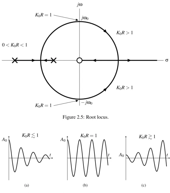
Figure 2.5: Root locus.
A0 K0R.1
t
(a)
A0 K0R=1
t
(b)
A0
K0R&1
t
(c)
Figure 2.6: Time solutions for amplitude (a) decay, (b) steady, and (c) growth.
Using (2.2) and K0 as a system parameter, we can plot the root locus and draw the same conclusion of (2.6), as shown in Fig. 2.5.
The time-domain solution of (2.5), for a loop gain near one,K0R≈1, is
vo(t)≈A0e−
(1−K0R)
RC tcos(ω0t), (2.7)
whereA0is the initial amplitude. From (2.7), or Fig. 2.5, three possible particular solution can be obtained, as shown in Fig. 2.6. For a loop gain slightly below unity,K0R.1, the oscillation can start, but cannot be maintained because the amplitude will decay exponentially until the oscillation stops. For a loop gain equal to unity,K0R=1, the loss inRis compensated, and the oscillation amplitude will be steady. For a loop gain with an excess,K0R&1, the oscillation amplitude will grow exponentially.
Negative-Resistance Resonator
K0vo
in vo i
C L R
(a)
+
−
1
K0i
vo i L
C
R
(b)
Figure 2.7: Negative-resistance model of (a) parallel, (b) seriesLC−oscillator.
Rearranging the circuit as shown in Fig. 2.7(a), it is clear that the resonator impedance is given by
Z(s) =Vo
I =
sC1 s2+sRC1 +LC1 ,
and the negative impedance is
ZN=
Vo
In
=− 1
K0.
Applying Kurokawa’s method,Z(s) =−ZN(s), yields the same characteristic equation
s2+s 1
RC(1−K0R) + 1 LC =0.
Therefore, we can conclude that, for linear systems, both methods give the same result. The dual circuit (Fig. 2.7(b)) yields a similar result for the current,i. For clarity, we will refer to the first as parallelLC−oscillator and to the second the seriesLC−oscillator.
In the seriesLC−oscillator, the impedance of the resonator is
Z(s) =Vo
I =sL+ 1 sC+R, and the impedance of the negative-resistance block is
ZN(s) =Vo
IN
=− 1
K0.
Applying again the Kurokawa’s method one obtains the characteristic equation
s2+sR L
1− 1
K0R
+ 1
LC =0, which yields the time-domain solution
i(t)≈A0e−
R L
1− 1
K0R
t
cos(ω0t). (2.8)
2 . 3 A M P L I T U D E C O N T RO L
+ Amplifier Oscillator
Peak detector
-Xre f Xout
Figure 2.8: Conceptually automatic amplitude control.
an amplitude control technique to reduce the loop gain to one,K0R=1 and to keep it at this value. In the next section such techniques are discussed in detail.
2.3
Amplitude control
Sinusoidal oscillators require an excess loop gain to ensure startup, leading to an exponential growth of the oscillation amplitude. The amplitude must be regulated, or controlled, to avoid unwanted harmonics and distortion due to the clipping. In Fig. 2.8, a conceptual diagram of an automatic amplitude control (AAC) based on a negative feedback of the amplitude is shown. This type of AAC circuit works as follows: the output amplitude is measured, using a peak detector, and compares it with a reference,Xre f. If the amplitude is larger than Xre f the oscillator’s gain
is proportionally reduced and if the amplitude is lower the gain is increased, until the amplitude stabilizes at the reference level, i.e.Xout ≈Xre f.
Using an AAC circuit, as the one of Fig. 2.8, has several advantages: it ensures a correct startup; allows to set the optimum gain to reduce the total harmonic distortion and minimize the phase noise [32]; it maintains a constant output power regardless of the resonator quality factor, temperature and process variations [32]. The phase noise flattening, as reported in [33, 34, 35], is also an advantage. However, an AAC circuit increases the oscillator complexity, requiring more power and die area, and can become unstable [36, 37]. Another important aspect, often neglected, is to ensure an independent amplitude and frequency control. Otherwise a multi-input multi-output (MIMO), or multivariable, controller is required which increases the controller complexity. TheLC−oscillator is an example in which the variable independence is guaranteed, since the frequency is determined only by the resonant tank and the amplitude can be controlled by the negative-resistance (usually controlled by the bias current). However, this is not the case for the majority ofRC−oscillators, which leads to a more complex controller, therefore limiting the use of this technique for this type of oscillator.
Another common method to control the amplitude, usually for lower frequencies, is to use clamping elements (with a nonlinear characteristics), e.g. rectifier diodes. In comparison with the above method, this solution leads to higher harmonic distortion [38].
Negative-Resistance Resonator
K0vo−K2v3o
in vo i
C ic
L R
Figure 2.9: Parallel Van der Pol oscillator.
the VDPO in which the negative-resistance block has a linear term,K0vo, and a nonlinear term,
K2v3o, as shown in Fig. 2.9. The first generates the negative-resistance and the later regulates the amplitude growth.
We present the VDPO because many modern oscillators have similar behaviour presenting an equivalent characteristic equation as shown in [26, 39, 40]. For this reason, in the next chapter, we will use the VDPO to study several types of coupling.
Next we study the stability of this amplitude control mechanism and derive the oscillator solutions.
2.3.1 Equilibrium points and stability
Although Kurokawa has presented in [30] the conditions for stability, we will use a more general method to study the stability of the VDPO in detail. Since the circuit has a nonlinearity, it is simpler to derive the system dynamics in the time domain, rather than working in the frequency domain. Applying the Kirchhoff’s current law at nodevowe obtain
Cdvo dt +
1 L Z
vodt+
vo
R =K0vo−K2v 3
o, (2.9)
that can be simplified to a nonlinear second-order differential equation by differentiating and dividing both sides by the capacitanceC
d2vo
dt2 + 1 RC
(1−K0R) +3K2Rv2odvo
dt + 1
LCvo=0. (2.10) Equation (2.10) can be reduced to the general form of the VDPO
d2vo
dt2 −2 δ0−δ2v 2
o
dvo
dt +ω 2
0vo=0, (2.11)
where δ0 = (K0R−1)/(2RC) andδ2 =3K2R/(2RC) represent the negative-resistance and the amplitude limiter, respectively,ω0is the oscillator free-running frequency.
2 . 3 A M P L I T U D E C O N T RO L
dvo
dt = 1
Cic (2.12a)
dic
dt =2 δ0−δ2v 2
o
ic+ω20vo (2.12b)
where the relation between the output voltage,vo, and the current of the capacitance,ic.
From (2.12) we can determine the equilibrium points, also known as critical points, by making the left-hand side of both equations zero. In this case, there is a single equilibrium point atic=0
andvo=0. An equilibrium point is where the system stays in equilibrium (assuming a noiseless
system). From the mathematical point of view, this means that an amplitude zero is a solution for (2.11). Physically it means that if the oscillator start with the capacitance and inductance discharged (voltage and current zero) it will remains in that state permanently.
We start by studying the local stability near the equilibrium point based on the linearised system. We find the linear version of the system, for any point in the phase space, calculating its Jacobian matrix
J=
" ∂f
∂vo
∂f
∂ic
∂g
∂vo
∂g
∂ic
#
⇒
"
0 C1
−4δ2icvo−ω20 2 δ0−δ2v2o
#
, (2.13)
where f is a function representing the derivative of the output voltage, f =dvo/dt, andgis a
function representing the derivative of the capacitance current,g=dic/dt.
From the eigenvalues of the linearised system (eigenvalues of the Jacobian matrix) we can determine its stability. The eigenvalues are the roots of the characteristic polynomial that is obtain from
|J−λI|=0⇒
0−λ C1
−4δ2icvo−ω02 2 δ0−δ2v2o
−λ
=0, (2.14) whereJis the Jacobian matrix (2.13),λis the eigenvalue andI is the identity matrix. From (2.14) we obtain the characteristic polynomial
λ2−Tλ+D=0, (2.15) whereT is the trace ofJandDis the determinant ofJ. For the VDPO the trace is
T =2 δ0−δ2v2o, (2.16) and determinant is
D= 1
C 4δ2icvo+ω 2
0. (2.17)
The stability conditions are: T<0 andD>0 for a stable point. For the equilibrium point at the origin we have
D(vo=0,ic=0) =
ω20
ic
vo
A
θ
Limit cycle Spiral source
Spiral sink
(a)
t vo
2qδ0
δ2
(b)
Figure 2.10: Van der Pol oscillator (a) phase diagram, (b) time-domain solution.
and
T(vo=0,ic=0) =2δ0>0, (2.19)
meaning that the equilibrium point is unstable if the trace of the Jacobian matrix is positive. Since δ0∼(K0R−1)we can safely say that the oscillation starts ifK0R>1, i.e. the equilibrium point
must be unstable. Furthermore, we can say that near the equilibrium point we have a spiral source, as shown in the phase diagram of Fig. 2.10(a), becauseT2<4D, resulting in two complex-conjugate eigenvalues. We can check this condition by solving (2.15) forλresulting
λ=T
2± 1 2
p
T2−4D, (2.20) which shows the eigenvalues expressed in terms of the trace,T, and determinate,D.
Since the system is an oscillator, we expect the existence of a stable limit cycle2. The existence of a stable limit cycle indicates that at some point, far from the equilibrium point, a spiral sink must exist beyond the limit cycle. A complex-conjugate eigenvalues withT <0 is a necessary
condition for the existence of a spiral sink. From (2.16) it is clear that if, and only if, the output voltage is abovevo>
p
δ0/δ2thenT <0 and, therefore, a spiral sink and a limit cycle exists. Based on the qualitative analysis of the VDPO, without explicitly determined the solution, we can conclude that the system has an unstable equilibrium point at the origin and a stable limit cycle that limits the oscillation amplitude, see Fig. 2.10(a). Since a stable limit cycle exists, the solution is a sinusoidal signal as shown in Fig. 2.10(b).
We can make a simpler qualitative analysis, assuming that the output signal,vois sinusoidal
vo(t) =A(t)cos(ω0t+φ). (2.21)
Using the harmonic balance method presented in [41], consisting of substituting (2.21) into (2.11) that is rewritten here for clarity,
2 . 3 A M P L I T U D E C O N T RO L
A
0 2qδ0
δ2
dA
dt
Repeller
Attractor
Figure 2.11: Amplitude curve of the Van der Pol oscillator.
d2vo
dt2 −2 δ0−δ2v 2
o
dvo
dt +ω 2 0vo=0,
the amplitude and phase derivatives are obtained, see Appendix B. Assuming a slow variation of the amplitude we obtain
dA
dt =δ0A− 1 4δ2A
3 (2.22a)
dφ
dt =0, (2.22b)
For the phase,φ, since its derivative is zero means that any constant phase is valid. The absolute phase value will depend on the initial conditions of the circuit and will be maintained indefinitely in steady-state.
For the amplitude, three equilibrium points:A=0,A=2pδ0/δ2andA=−2pδ0/δ2can be determined from Section 2.3.1. However, we will consider only positive values for the amplitude since the negative values can be represented by a phaseφ=π. The plot of (2.22a) is shown in Fig. 2.11. A qualitative analysis of (2.22a) and Fig. 2.11, shows that the equilibrium pointA=0 is
unstable, becausedA/dt>0 forA>0, meaning that the oscillator can start with a zero amplitude, but any deviation from the equilibrium point and the amplitude will increase, and it never goes back. The second equilibrium pointA=2pδ0/δ2is an attractor because for an amplitude below the equilibrium pointdA/dt>0 and for amplitudes above the equilibrium pointdA/dt>0. We also know that this attractor is stable because it is related to the stable limit cycle determined before, see Fig. 2.10(a).
The (2.22) can also be used to obtain the analytical solution for the amplitude since it is a separable first-order equation [41]. The general solution is given by
Z 1
δ0A−14δ2A3dA=
Z
I
levelM
5M
6v
i=
−
v
oR
NIlevel
2
+
i
o Ilevel2−
i
oFigure 2.12: Negative resistance circuit.
1 2δ0ln
4A2
4δ0−δ2A2
=t−T0,
from which results the transient amplitude response
A(t) =2
s
δ0
δ2+A0e−2δ0t,
(2.23)
whereA0=4δ−01e2δ0T0 is a parameter that defines the initial amplitude of the circuit, i.e. fort=0. For steady-state, i.e.t→∞, the oscillation amplitude given by (2.23) is reduced to
A=2 s
δ0
δ2. (2.24)
The solution for the parallel topology of VDPO withK0R>1 is obtained by substituting (2.23) into (2.21) resulting
vo(t) =2
s
δ0
δ2+A0e−2δ0tcos(ω0t+φ).
A similar solution for the series topology is obtained. Notice however that the result is expressed in terms of the current and not the voltage.
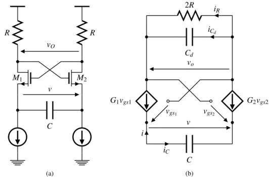
2.3.2 Negative-resistance circuits
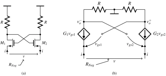
In modern oscillators the negative-resistance is often implemented by a cross-coupled differential pair, as shown in Fig. 2.12. Here, we discard the capacitances,CgsandCgd, of transistorsM1and
M2, since they can be lumped with the oscillator capacitance,C, resulting the simplified signal model of Fig. 2.13. From Fig. 2.13 we obtain
io=−G1vgs1 (2.25a)
io=G2vgs2 (2.25b)
2 . 3 A M P L I T U D E C O N T RO L
G
1v
gs1G
2v
gs2i
oi
oR
Nv
i=
−
v
ov
gs1v
gs2Figure 2.13: Negative resistance small-signal equivalent circuit.
Substituting (2.25a) and (2.25b) into (2.25c) we obtain the equivalent circuit resistance
RN=
v
i =−
G1+G2
G1G2 . (2.26)
whereGiis the signal dependent transconductance of thei−th transistor, modelled by
Gi=gm0+2Kvgsi, (2.27)
where K is a parameter dependent on the transistors dimensions and technology, gm0 is the
transistors’ transconductance assuming no mismatch andvgsiis the gate to source voltage of the
i−th transistor, see Appendix A. In differential mode we get
vgs1=
vi
2 (2.28a)
vgs2=−vi
2. (2.28b)
Substituting (2.28) into (2.27) and (2.26) results the, approximated, resistance of the circuit of Fig. 2.12
RN≈
2
−gm0+ K
2
gm0v 2
i
, (2.29)
where it is clear thatRNegis a negative resistance in parallel with a nonlinear resistance that depends
on the incremental voltage,v2i.
Another negative-resistance circuit often used is shown in Fig. 2.14(a). From its small-signal equivalent circuit (Fig. 2.14(b)) we obtain
i=−G1vgs1 (2.30a)
i=G2vgs2 (2.30b)
vo=v+o −v−o =−2Ri (2.30c)
M1 M2
R R
i i
v
RNeg
(a)
G1vgs1 G2vgs2
R R
vgs1 vgs2
i i
v−o v+o
RNeg
v
(b)
Figure 2.14: Negative resistance circuit (a) and the small-signal equivalent (b).
Substituting (2.30a), (2.30b) and (2.30c) into (2.30d) and rearranging the equation results the equivalent resistance of the circuit
RNeg=
v
i =
G1+G2 G1G2
−2R=2 1
gm0−gKm20v2− R
!
, (2.31)
From (2.31) we conclude that the equivalent resistance of the circuit (Fig. 2.14(a)) is a negative resistance in series with a nonlinear positive resistance. Because of this, instead of the parallel, the series VDPO approximation is used.
2.4
Frequency selectivity
The oscillation frequency of a sinusoidal oscillator is forced by the resonator. From the feedback model perspective, the resonator makes the required phase-shift so that the loop gain phase be 2π at the oscillation frequency. For the negative-resistance model, the resonator is a band-pass filter that attenuates unwanted frequencies passing only the frequency of its resonance,ω0. This usually forces a free-running oscillator, like those we study so far, to have an oscillation frequency equal to the resonant frequency, or close to it if we consider the circuit’s parasitic elements. However, that is not the case for coupled oscillators, as we will show in the following chapters.
2 . 4 F R E Q U E N C Y S E L E C T I V I T Y
noise spectrum shape is modelled by the equation proposed by Leeson in [42]. The phase noise along withQare the common figures of merit for oscillators. Here, we will not discuss the phase noise topic; a comprehensive description can be found in [2, 3, 9, 11, 43]. We will focus on the definitions ofQand their equivalences.
In literature [2, 3], the general definition of theQis
Q=2π Maximum Energy stored
Energy dissipated per cycle, (2.32) which physically means the number of oscillations that a resonator does with the maximum energy stored in one cycle. From the general definition, we can derive theQof a resonator network. For the parallelRLCresonator the voltage is the same for all elements. Hence, the maximum energy stored per cycle is related to the maximum voltage,A, on the capacitor, so that
EC=
1 2CA
2
, (2.33)
whereAis the oscillation amplitude (maximum voltage). The energy dissipated per cycle in the resistor is
ER=
Z T
0 P(t)dt=
Z T
0 v2(t)
R dt,
where v(t) =Acos(ω0t), T is the oscillation period and R is the resistance value. Using the trigonometric identity cos2ω0t=1
2(1+cos 2ω0t)we get
ER=
1 2
1 RA
2T. (2.34)
Substituting (2.33) and (2.34) into (2.32) results the well-known quality factor of the parallel RLCcircuit
Q=2π 1 2CA2 1 21RA2T
=ω0RC=R r
C
L. (2.35)
For the series RLC resonator it is the current that is common to all elements. Hence, the maximum energy stored per cycle is related to the maximum current in the inductor
EL=
1 2LA
2, (2.36)
whereAis the amplitude of the current. Reusing the energy dissipation equation so that
ER=
Z T
0 Ri 2(t)
dt=1
2RA
2T. (2.37)
Substituting (2.36) and (2.37) into (2.32) results
Q=2π
1 2LA2 1 2RA2T
=ω0L
R=
1 R
r L
C. (2.38)
1 √ 2 1
|H(jω)β(jω)| K0R
≈1
ω1 ω0 ω2
∆ω
-3dB
ω
Figure 2.15: Loop gain frequency response.
easily grouped e.g. microwave circuits. However, if the exactQcannot be determined, it should be measurable. In 1966 Leeson presented in [42] another definition forQthat solves this problem. The Leeson’s definition relates the resonant frequency and the -3dB bandwidth of the resonator
Q= ω0
∆ω, (2.39)
where ω0 is the resonant frequency and ∆ω is the -3dB bandwidth. This definition allows to measure theQfrom the resonator’s frequency response. No formal proof was presented in [42]. The proof that both definitions are equivalent was derived in [44]. Take the loop gain of the LC−oscillator of Section 2.2, that we rewrite here for clarity, and assumeK0R≈1
H(s)β(s) = s
1
RC
s2+sRC1 +LC1 ,
make the square of its magnitude equal to 12
|H(jω)β(jω)|2= ω
2 1
RC
2
ω20−ω22+ω2 RC1 2 =
1 2,
which is equivalent to a -3dB attenuation of the loop gain, as shown in Fig. 2.15. Solving forωwe obtain the polynomial
ω2±ω 1
RC−ω
2 0=0, with the positive roots:
ω1=−2RC1 +
q 1
RC
2
+4ω2
0, ω2=2RC1 +
q 1
RC
2
+4ω2 0,
2 . 4 F R E Q U E N C Y S E L E C T I V I T Y
∆ω=ω2−ω1= 1
RC. (2.40)
Substituting (2.40) into (2.39) forω=ω0results
Q=ω01 RC
=R r
C
L, (2.41)
which is equal to (2.35). Hence, we can conclude that both definitions yield the same result for second order resonators [2]. A similar conclusion can be drawn for the series RLC resonator. However, for oscillators with distributed elements, which cannot be reduced to a second-orderRLC circuit, the Leeson definition forQis not accurate, as explained in [11, 45].
A third definition in Clarke-Hess [44] and in Rhea [46], based on the feedback model, defined Qas the phase slope at the resonance frequency
Q=−1
2ω0 ∂θ
∂ω,
latter it was showed that this definition only can be applied to oscillators with resonators since it only considers the phase for the frequency stability. The definition fails for resonatorless oscillators like the two-integrator and the phase-shift oscillator [11].
A fourth definition proposed by Razavi in [11], called the open-loopQ, is based on the open-loop gain derivatives of the magnitude and phase,
Q=ω0
2 s
dA dω
2
+
dθ dω
2
, (2.42)
whereAis the magnitude andθis the phase of the loop gain. This definition is especially useful for analysis using the feedback model. A similar definition based on the Rhea definition, was proposed by Randall and Hock in [47], using the phase slope or group delay to determine the quality factor. They use the S-parameters to describe the open loop gain and from it theQ.
More recently, the definition proposed by Razavi was extended by Ohira in [48] and generalized to one- and two-port passive networks and in [49] to active networks as well. Ohira defines theQ factor as "the logarithmic derivative of port impedance"
Q=ω0
2
d
dωln(Z(jω))
=
ω0 2
1
|Z|
dZ dω
, (2.43)
whereZis the resonator impedance. Using the resonators impedance presented in Section 2.2 we can verify the equivalence between the Ohira’s definition and the other four definitions. Starting with the seriesRLCresonator, we know that the impedance is
Z(s) =sL+ 1
sC+R, usings= jωthe magnitude of the impedance is
|Z(jω)|=
s
ωL− 1
ωC 2
and the derivative is
dZ
(jω)
dω =
L+ 1
ω2C
=
ω2LC+1
ω2C
. (2.45)
Substituting (2.44) and (2.45) into (2.43) withω=ω0results the expectedQof a seriesRLC circuit
Q= ω0
2 1 R
2
ω20C=
1 R
r L C.
For the parallelRLC, the impedance is
Z(s) = s
1
C
s2+sRC1 +ω20, usings= jωthe magnitude of the impedance is
|Z(jω)|= ω
1
C
q
ω20−ω22+ω2 RC1 2
, (2.46)
and the derivative is
dZ
(jω)
dω
=2R2C. (2.47) Substituting (2.46) and (2.47) into (2.43) withω=ω0results the expectedQof a parallelRLC circuit
Q=ω0
2 1 R2R
2C=R r
C L.
The fifth method yield the same result for second order resonators, therefore, we can conclude that they are equivalent. Since we will use the VDPO as a basic oscillator to study the coupled oscillators it is pertinent to write the Van der Pol equation in terms ofQ. Writing the VDPO in terms ofQyields an advantage since the series and parallel topologies can be described by a single equation. The VDPO coefficientsδ0andδ2are described in terms ofQas:
δ0= ω0
2Q(K0R−1),δ2=
ω0
2Q(3K2R), from which the characteristic equation is
s2+ω0
Q
(K0R−1) +3K2RA2s+ω20=0,
and the differential equations is
d2xo
dt2 + ω0
Q
(K0R−1) +3K2Rx2odxo
dt +ω 2 0xo=0,
C
H
A
P
T
E
R
3
I
N J E C T I O N
L
O C K I N G
Contents
3.1 Introduction . . . 27 3.2 Parallel VDPO . . . 29 3.3 Series VDPO . . . 34 3.3.1 Single external source . . . 35 3.3.2 Double external source . . . 37 3.4 Conclusion . . . 38
3.1
Introduction
In Chapter 2 we studied the series and parallel topology of sinusoidal oscillators in free-running mode, in which the oscillator input is zero. In this chapter we study a more general case, known as driven mode, in which the oscillator input is connected to an external periodic signal generator (a nonzero input). We use the VDPO to study the coupling and derive the equations for the oscillation frequency, amplitude, and phase. We consider both the series and parallel topologies of the VDPO since we want to apply the results to the study of the coupledRC−oscillator (which is modelled by the series VDPO) and the Two-Integrator (modelled by the parallel VDPO). We start by describing the synchronization of a single oscillator with an external sinusoidal source, then in the following chapters we substitute the external source by a second oscillator and study its influence on the quadrature oscillator key parameters.
2π
ωinj−ω0
2π
ωinj+ω0
t
Figure 3.1: Beat.
be locked with a sub-harmonic of its free-running frequency, thus implementing a divide-by-two or divide-by-three circuit, as explained in [53]. Another useful application is the improvement of an oscillator noise by direct injection the signal of a reference oscillator (with low phase-noise); the advantage of this method is the reduction of the phase-noise without requiring additional circuits and power. A comprehensive study of the above applications can be found in [52]. In this chapter we focus on using the injection-locking theory to study coupled oscillators.
Injection-locking occurs when an oscillator is driven by an external periodic signal (locking signal) and the injected current, or voltage, forces the oscillator to change its frequency, synchronizing it with the locking signal. However, this synchronization only occurs if the locking frequency is within a band (dependent of the oscillator parameters), commonly known as locking range. Otherwise, if the frequency is either below or above the locking range, the output will be a high frequency sinusoid (with the sum of the external and free-running frequencies) modulated in amplitude by a low frequency sinusoid (the difference between the two frequencies), as shown in Fig. 3.1. This phenomenon is called Beat.
The locking range is an important parameter also for coupled oscillators because practical oscillators have mismatches and their oscillation frequencies may diverge. The mismatches and the parasitic elements should not separate the oscillation frequencies beyond the locking range, otherwise the locking between the two oscillators does not occur, leading to an undesired output signal, as shown in Fig. 3.1.
3 . 2 PA R A L L E L V D P O
iinj K0v−K2v3 C
iC
L iL
R iR
i
v
Figure 3.2: Injection-lock parallel VDPO
3.2
Parallel VDPO
In this section we study the injection-lock in the parallel VDPO. The results obtained here will be relevant to the study of the two-integrator oscillator, in Chapter 6, which consists of two integration stages coupled by transconductance amplifiers. The two-integrator oscillator can be modelled by two injection-locked stages, in which the output of a stage will drive the injection current on the other.
Let us analyse the parallel VDPO with an external sinusoidal current source (locking signal) in parallel, as shown in Fig. 3.2. Applying the Kirchhoff’s current law (KCL) we obtain
iC+iR+i+iL=iinj,
substituting the currents by their equations we get
Cdv dt +
1
Rv−K0v+K2v 3
+1
L Z
vdt=iinj,
Dividing both sides of the equation byCand differentiating one obtains
d2v
dt2−2 δ0−δ2v 2dv
dt +ω 2
0v=ω0R Q
diinj
dt , (3.1)
where
δ0= ω0
2Q(K0R−1), δ2= ω0 2Q3K2R,
andQis the quality factor of the parallelRLCcircuit. We call (3.1) the driven VDPO equation because the right-hand side is non zero. In mathematical terminology, this is a non-homogeneous differential equation.
From differential equations theory, we know that the general solution of a linear differential equation is the solution of the homogeneous equations,vH, plus the particular solution of the
non-homogeneous,vP
v(t) =vH(t) +vP(t). (3.2)
near the steady-state. Hence, assuming that the system is near steady-state and knowing that the solution is sinusoidal, (3.2) can be written as
v(t) =Vsin(ωt−φ) = (VH+VP)sin[ωt−(φH+φP)], (3.3)
whereVH andφH are the amplitude and phase of the homogeneous solution,VP andφP are the
amplitude and phase of the particular solution. The amplitude and phase derivatives of the homogeneous solution were already derived in (2.22) and the result is
dVH
dt =δ0VH− 1 4δ2V
3
H (3.4a)
dφH
dt =0. (3.4b)
To obtain the particular solution we first have to match the left- and right-hand sides of (3.1), writing the latter in terms of sinωtand cosωt. To do this, we assume a locking signal of the form
iinj=Iinjsin ωinjt−φinj. (3.5)
Using the trigonometric relationship cos(α+β) =cosαcosβ−sinαsinβin the derivative of (3.5), result in
diinj
dt =Iinjωinj
cos Ωt−φinjcosωt−sin Ωt−φinjsinωt, (3.6) whereΩ= ωinj−ωis the frequencies difference (it is zero when there is locking). Substituting (3.6) into (3.1) and, using the harmonic balance method, and neglecting the second term of (3.1) (see Appendix C for details) we obtain the amplitude and phase derivatives of the particular solution: dVP dt = ω0 Q · ωinj
2ω ·RIinjcos
ωinj−ωt+φ (3.7a) dφP
dt =
ω2−ω20
2ω − ω0 Q · ωinj 2ω · RIinj V sin
ωinj−ωt+φ, (3.7b)
whereφis the phase difference between the oscillator output and the locking signal. From (3.4) and (3.7) we obtain the amplitude and phase derivatives of the general solution
dV dt =
δ0V−1
4δ2V
3+ω0ωinj
2Qω RIinjcos
ωinj−ωt+φ (3.8a)
dφ dt =
ω2−ω20
2ω −
ω0ωinjRIinj
2QωV sin
ωinj−ω
t+φ. (3.8b)
3 . 2 PA R A L L E L V D P O
π
2 π 32π 2π
ω0Iinj
2QIosc
ω
inj =
ω 0
P 0
Unlocked
ω,ωinj
Locked
ω=ωinj
φ dφ
dt
(a)
t0 φ
iinj
v
t
(b)
Figure 3.3: Phase curve of the injection-lock parallel VDPO (a) and the time solution of path path P (b).
Assuming that the oscillator is lockedω=ωinj, (3.8) becomes
dV dt =
δ0V−1
4δ2V
3+ω0
2QRIinjcos(φ) (3.9a) dφ
dt =
ω2inj−ω20
2ωinj −
ω0 2Q·
Iinj
I sin(φ). (3.9b) whereIis the oscillator’s bias current (Figure 3.2).
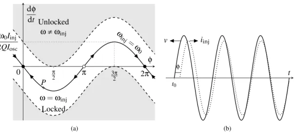
We analyse first the phase derivative given by (3.8) and illustrated in Fig. 3.3(a). In Fig. 3.3(a) the locking region (in which the oscillator frequency equals the locking frequency) is represented in white and the unlocking regions (whereω,ωinj) are shaded. The dashed curves represent the
boundary between the unlocking and locking regions. To better understand the circuit behaviour, consider the particular case of a locking signal with the same frequency of the free-running oscillator, ωinj=ω0, (represented in the figure by the solid curve). From (3.9) we find two
equilibrium points: a stable equilibrium point atφ=0 and an unstable atφ=π. Hence, in steady-state, the locking signal and the oscillator output will be in-phase.
Let us consider the signals of Fig. 3.3(b) with a phase differenceφ=π/3, which corresponds to
pointPin the phase curve of Fig. 3.3(a). At this point, the phase derivative is negative meaning that the oscillator phase will be forced to decrease until both signals are in-phase. Hence, as time passes the phase difference is reduced, as shown in Fig. 3.3(b). If we consider a phase difference higher thanπthe derivative is positive meaning that the phase will increase until it reaches aφ=2π.
From (3.9) we can see that the other curves (that will be within the white region) are offset versions of this particular case. For ωinj >ω0 the curve is shifted upwards and the stable
equilibrium point shifts to the right (increasing the phase difference). Forωinj<ω0 the curve is
ω0−∆ω
2 ω0+
∆ω
2
−π2
π
2
ω0
QI
ω0Iinj
ωinj
φ
Figure 3.4: Injection Lock phase curve.
until the high boundary is reached (higher dashed curve). At this point a single equilibrium point exists (atφ=π/2), but it is unstable, meaning that the oscillator cannot follow further the locking signal and enters the unlocking region. This frequency is the upper limit of the locking range,∆ω. On the opposite direction, if we decrease the frequency until the bottom limit is reached, the same happens (the only difference is that the unstable equilibrium point is atφ=3π/2=−π/2). From (3.9), we can analytically determine the locking range by equating the left-hand side to zero and solving toωinjfor the two boundary cases. Hence, forωinj<ω0andφ=−π/2,
ω2inj.min+ω0
Q · Iinj
I ωinj.min−ω 2
0=0, (3.10) so that the positive root is
ωinj.min=−
ω0 2Q
Iinj
I +
1 2
s 1
2Q Iinj
I 2
ω20+4ω20. (3.11)
Forωinj>ω0andφ=π/2,
ω2inj.max−ω0
Q · Iinj
I ωinj.max−ω 2
0=0, (3.12) so that the positive root is
ωinj.max=
ω0 2Q
Iinj
I +
1 2
s 1
2Q Iinj
I 2
ω20+4ω20. (3.13)
The difference between the maximum (3.13) and minimum (3.12) frequencies gives the locking range
∆ω=ωinj.max−ωinj.min=ω0 Q
Iinj
3 . 2 PA R A L L E L V D P O
−2qδ0
δ2 2
q
δ0
δ2 2
r
δ0+
ω0Iinj
2QI
δ2
ω0Iinj
2Q
φ=0
φ=±π2
0
V dV
dt
Figure 3.5: Amplitude phase curve of the injection locking
which is consistent with the locking range equation in [52].
By taking again (3.9), equating the left-hand side to zero, and solving the equation forφwe get
φ=arcsin Q
ω0 I Iinj
ω2inj−ω20
ωinj
!
, (3.15)
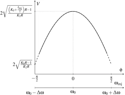
which relates the phase difference with the frequency of the locking signal, as shown in Fig. 3.4. From Fig. 3.4 we can see that the phase difference decreases with the increase of the locking frequency. Near the free-running frequency,ω0, the characteristic is almost linear with slope ωQI0I
inj.
Note that the graph in Fig. 3.4 is not defined for frequencies outside the locking range, since the oscillator is not locked and the phase is not constant.
Let us analyse now the amplitude derivative given by (3.8) and illustrated in Fig. 3.5 where the shaded areas correspond to states where the oscillator is unlocked. The white area corresponds to states where the oscillator is locked (3.9). We rewrite it here for convenience
dV dt =
δ0V−1
4δ2V
3+ω0