Novembro, 2014
Pedro de Abreu Avó Baião
Licenciado em Ciências de Engenharia de Materiais
Nanostructuring silicon probes via electrodeposition:
Characterization of electrode coatings for acute
in vivo
neural recordings
Dissertação para obtenção do Grau de Mestre em
Engenharia de Micro e Nanotecnologias
Orientador: Adam Kampff, Professor Doutor, Champalimaud Center for the Unknown
Co-orientador: Elvira Fortunato, Professora Doutora,
Faculdade de Ciências e Tecnologia da Universidade Nova de Lisboa
Júri:
Presidente: Prof. Doutor Rodrigo Ferrão Paiva Martins
i
NANOSTRUCTURING SILICON PROBES VIA ELECTRODEPOSITION: CHARACTERIZATIONOF ELECTRODE COATINGS FOR ACUTE IN VIVO NEURAL RECORDINGS
NANOSTRUCTURING SILICON PROBES VIA
ELECTRODEPOSI-TION: CHARACTERIZATION OF ELECTRODE COATINGS FOR
ACUTE
IN VIVO
NEURAL RECORDINGS
Copyright © Pedro de Abreu Avó Baião
Faculdade de Ciências e Tecnologia
Universidade Nova de Lisboa
ii
NANOSTRUCTURING SILICON PROBES VIA ELECTRODEPOSITION: CHARACTERIZATIONiii
NANOSTRUCTURING SILICON PROBES VIA ELECTRODEPOSITION: CHARACTERIZATIONOF ELECTRODE COATINGS FOR ACUTE IN VIVO NEURAL RECORDINGS
So the future is like a huge freight train barreling down the tracks, headed our way. Be-hind this train is the sweat and toil of thousands of scientists who are inventing the future in
their labs. You can hear the whistle of the train. It says: biotechnology, artificial intelligence,
nanotechnology, and telecommunications. However, the reaction of some is to say, “I am too old. I can’t learn this stuff. I will just lie down and get run over by the train.” However, the
re-action of the young, the energetic, and the ambitious is to say, “Get me on that train! This train
represents my future. It is my destiny. Get me in the driver’s seat.”
iv
NANOSTRUCTURING SILICON PROBES VIA ELECTRODEPOSITION: CHARACTERIZATIONv
NANOSTRUCTURING SILICON PROBES VIA ELECTRODEPOSITION: CHARACTERIZATIONOF ELECTRODE COATINGS FOR ACUTE IN VIVO NEURAL RECORDINGS Acknowledgements
I would like to thank everyone who have made this dissertation possible. It has been a trying and interesting time in my life. I know and I’m truly sorry for not mentioning everyone that fully supported me on this project and throughout my bachelors and master’s degree. But with that said, I dearly hope I’m able to make justice to everyone by honoring and paying tribute to them here. I would like to highlight and sincerely thank the following:
To Dr. Adam Kampff for giving me the chance to work alongside an amazing team at the Champalimaud Center of the Unknown (CCU) and an experience that will not be forgotten. It truly was an amazing opportunity to elaborate on such an interesting and daring topic with the possibility to contribute on improving further knowledge in this research field. I would also like to express my gratitude for the useful comments, remarks and engagement through the learning process of this master thesis.
To Prof. Elvira Fortunato from the moment I attended her Microelectronic I lectures till the moment was given complete trust to extend my work beyond CENIMAT/I3N. Also, being allowed work in her research group having full support and guidance. Along with Prof. Rodrigo Martins, and by putting a tremendous effort, expertise and passion for science, they built fully equipped laboratories and established crucial relations with national and international partners, creating the scientific and financial basis that allowed this and many other research works to be developed.
To Joana Neto for allowing me to work alongside her and continue to explore her work. The tremendous patience for inserting me in a topic I was completely oblivious and guiding me every day from the start till the end of my dissertation. Without her this project wouldn’t have been possible and I’m truly grateful for what she thought me and for the enormous help tackling many of the scientific and practical hurdles we’ve encountered along the way.
To Kinga Kocsis for being so helpful and having such an enormous patience in analyzing surgery recordings and introducing spike sorting methods. Data analysis would have been so much easier if you had been in Portugal helping us from the start of this project. Thank you
so
much
for the tremendous help you’ve offered and provided.I would also like to thank the rest of the members of the Intelligent Systems Lab at the CCU who I was proud to work alongside and discuss many topics with: George Dimitriadis, Gonçalo Lopes, Joana Nogueira, João Frazão and Pedro Lacerda.
vi
NANOSTRUCTURING SILICON PROBES VIA ELECTRODEPOSITION: CHARACTERIZATIONOF ELECTRODE COATINGS FOR ACUTE IN VIVO NEURAL RECORDINGS
To Lídia Santos for her insights on tungsten oxide synthesis and always being ready to help when needed. Together with Dra. Rita Branquinho, I was able to fully comprehend the elec-trochemical phenomena occurring on this project.
To everyone at CENIMAT/I3N that provided me a great work environment and an amaz-ing experience.
To my colleagues and friends who I’ve met at Faculdade de Ciências e Tecnologia (FCT) and who’ve accompanied me from the start of my bachelor’s in Materials Science until the end of my master’s in Micro and Nanotechnology: Alexandre Oliveira, Ana Catarina, Ana Kullberg, Ana Paula, Ana Rita, Daniel Matos, Gonçalo Rodrigues, Joana Fernandes Miguel Soares, Paul Grey, Pedro Loures, Ricardo Marreiros, Rita Pontes, Rute Almedia and Vasco Rodrigues. Also to my long date friends who’ve accompanied from my early stages till this moment: André Pontes and Luis Marques. Thanks for all the moments filled with stupidity and joy.
I would like to thank my loved ones, starting with my family, who have supported me throughout the entire process. To my mom and grandmother for putting up with me for the past 24 years and for making me the man I am today. A moment I truly want to dedicate to them. To my father, his wife and my siblings for their understanding in my absence in their lives and for the strength they gave me throughout the years.
vii
NANOSTRUCTURING SILICON PROBES VIA ELECTRODEPOSITION: CHARACTERIZATIONOF ELECTRODE COATINGS FOR ACUTE IN VIVO NEURAL RECORDINGS
Resumo
Para compreender o funcionamento do cérebro são necessárias ferramentas capazes de medir a atividade elétrica de neurónios a uma grande escala. Todavia, são necessários progressos para aumentar o número de neurónios registados e identificados simultaneamente com microeléctrodos existentes. Este projeto tem como objetivo avaliar como diferentes materiais podem modificar a eficiência da transferência de sinal entre o tecido neuronal e elétrodos.
Dessa forma, diversos materiais para revestimento (ouro, PEDOT, óxido de tungsténio, nanotubos de carbono) foram caracterizados em termos dos fenómenos eletroquímicos e eficiência de aquisição de sinal. Elétrodos de irídio (177-706 μm2) foram revestidos através de deposições galvanostáticas sob diferentes densidades de carga.
Através de espectroscopia de impedância (EIS) em solução salina foi determinado que o módulo da impedância a 1 kHz depende do material de revestimento e diminui um máximo de duas ordens de magnitude para PEDOT (1 MΩ para 25 kΩ). Os elétrodos foram também caracterizados por voltametria cíclica (CV) demonstrando um aumento de uma ordem de magnitude na capacidade de armazenamento de carga, alcançando um máximo de 84.1 mC/cm2 para o compósito PEDOT:nanopartículas de ouro (aumento de 38 vezes na capacidade).
Gravação da atividade neuronal espontânea no córtex foi efetuada em roedores anestesiados para avaliar o desempenho dos revestimentos de elétrodos.
viii
NANOSTRUCTURING SILICON PROBES VIA ELECTRODEPOSITION: CHARACTERIZATIONix
NANOSTRUCTURING SILICON PROBES VIA ELECTRODEPOSITION: CHARACTERIZATIONOF ELECTRODE COATINGS FOR ACUTE IN VIVO NEURAL RECORDINGS
Abstract
Understanding how the brain works will require tools capable of measuring neuron elec-trical activity at a network scale. However, considerable progress is still necessary to reliably increase the number of neurons that are recorded and identified simultaneously with existing mi-croelectrode arrays. This project aims to evaluate how different materials can modify the effi-ciency of signal transfer from the neural tissue to the electrode.
Therefore, various coating materials (gold, PEDOT, tungsten oxide and carbon nano-tubes) are characterized in terms of their underlying electrochemical processes and recording ef-ficacy. Iridium electrodes (177-706 μm2) are coated using galvanostatic deposition under different charge densities.
By performing electrochemical impedance spectroscopy in phosphate buffered saline it is determined that the impedance modulus at 1 kHz depends on the coating material and decreased up to a maximum of two orders of magnitude for PEDOT (from 1 MΩ to 25kΩ). The electrodes are furthermore characterized by cyclic voltammetry showing that charge storage capacity is im-proved by one order of magnitude reaching a maximum of 84.1 mC/cm2 for the PEDOT: gold nanoparticles composite (38 times the capacity of the pristine).
Neural recording of spontaneous activity within the cortex was performed in anesthetized rodents to evaluate electrode coating performance.
x
NANOSTRUCTURING SILICON PROBES VIA ELECTRODEPOSITION: CHARACTERIZATIONxi
NANOSTRUCTURING SILICON PROBES VIA ELECTRODEPOSITION: CHARACTERIZATIONOF ELECTRODE COATINGS FOR ACUTE IN VIVO NEURAL RECORDINGS Symbols
A Area of the electrodes (μm2)
CH Helmholtz capacitance (F)
CPE1 Constant phase element 1 (S.s1/2)
CPE2 Constant phase element 2 (S.s1/2)
CPE3 Constant phase element 3 (S.s1/2)
Csc Charge storage capacity (mC/cm2)
DOHP Distance to the Outer Helmholtz Plane
ε0 Vacuum permittivity (F/m)
εr Relative static permittivity (a.u)
n Phase of the CPE
P2Pavg Peak to Peak average amplitude value (μV)
RE Resistance of the electrolyte seen by the electrode (Ω) Rp Resistance of the porous structure (Ω)
RCT1 Charge transfer resistance 1 (Ω) RCT2 Charge transfer resistance 2 (Ω) SNR Signal to noise ratio (a.u)
STDV Standard deviation (μV)
Y0 Adjustable parameter containing the diffusion coefficient (S.s1/2)
Y0CPE1 Adjustable parameter containing the diffusion coefficient 1 (S.s1/2)
Y0CPE2 Adjustable parameter containing the diffusion coefficient 2 (S.s1/2)
Y0CPE3 Adjustable parameter containing the diffusion coefficient 3 (S.s1/2)
ω Angular frequency (rad/s)
W Warburg diffusion element (S.s1/2)
Z Impedance (Ω)
Zac Impedance value after coating (Ω)
Zdrop Impedance drop from the initial value to post-coating value (a.u)
Zi Impedance value before coating (Ω)
xii
NANOSTRUCTURING SILICON PROBES VIA ELECTRODEPOSITION: CHARACTERIZATIONxiii
NANOSTRUCTURING SILICON PROBES VIA ELECTRODEPOSITION: CHARACTERIZATIONOF ELECTRODE COATINGS FOR ACUTE IN VIVO NEURAL RECORDINGS Abbreviations
Au Gold
ALS Amyotrophic Lateral Sclerosis
Au NPs Gold Nanoparticles
C Carbon
Cl Chlorine
CNT Carbon Nanotubes
CV Cyclic Voltammetry
DLS Dynamic Light Scattering
ECM Extracellular membrane
EEG Electroencephalography
EF Extracellular Fluid
EDL Electrochemical Double Layer
EIS Electrochemical Impedance Spectroscopy
ECEI Electrode-Coating-Electrolyte Interface
fMRI functional Magnetic Resonance Imaging
FETs Field Effect Transistors
HDP High Density Probe
MEMS Microelectromechanical Systems
MW Multi-Wall
Na Sodium
O Oxygen
PEDOT Poly(3,4-ethylenedioxythiophene)
PET Positron Emission Tomography
P2P Peak-To-Peak Amplitude
PSS Poly(styrenesulfonate)
PVP Polyvinylpyrrolidone
R.E Reference Electrode
xiv
NANOSTRUCTURING SILICON PROBES VIA ELECTRODEPOSITION: CHARACTERIZATIONOF ELECTRODE COATINGS FOR ACUTE IN VIVO NEURAL RECORDINGS SDS Sodium Dodecyl Sulfate
SEM Scanning Electron Microscopy
Si Silicon
W Tungsten
XRD X-Ray Diffraction
WO3 Tungsten Oxide
WO3 NPs Tungsten Oxide Nanoparticles
xv
NANOSTRUCTURING SILICON PROBES VIA ELECTRODEPOSITION: CHARACTERIZATIONOF ELECTRODE COATINGS FOR ACUTE IN VIVO NEURAL RECORDINGS
Table of Contents
1. INTRODUCTION ... 1
1.1.OVERVIEW ... 1
1.2.ELECTRODE-TISSUE INTERFACE ... 3
1.3.ELECTRODE MODIFICATIONS ... 4
2. MATERIALS AND METHODS ... 7
2.1. SOLUTION-BASED SYNTHESIS ... 7
2.2.1. Commercial gold solution ... 7
2.1.2. Tetrachloroauric acid solution (HAuCl4) – Polyvinylpyrrolidone (PVP) ... 7
2.1.3. Gold nanoparticles (Au NPs) ... 7
2.1.4. Poly(3,4-ethylenedioxythiophene) – Poly(styrenesulfonate) (PEDOT:PSS) . 7 2.1.5. Tungsten oxide nanoparticles (WO3 NPs) ... 7
2.1.6. Carbon Nanotubes – Sodium dodecyl Sulfate (CNTs:SDS) ... 8
2.1.7. Carbon Nanotubes – Poly(3,4-ethylenedioxythiophene) composite (CNTs:PEDOT) ... 8
2.1.8. Gold Nanoparticles - Poly(3,4-ethylenedioxythiophene) composite (Au NPs:PEDOT) ... 8
2.2. SOLUTION CHARACTERIZATION ... 8
2.2.1. X-Ray Diffracion (XRD) ... 8
2.2.1. Dynamic Light scattering (DLS) ... 8
2.2.3. Scanning Electron Microscopy (SEM) ... 9
2.3. SILICON PROBES ... 9
2.3.1. Silicon probe characterization ... 9
2.3.2. Electrochemical characterization ... 9
2.3.3. Morphological characterization ... 9
2.3.4. Electrodeposition set-up ...10
2.4. ACUTE RECORDINGS ... 10
3. RESULTS ... 13
3.1. SOLUTION CHARACTERIZATION... 13
3.1.1. Au NPs ...13
3.1.2. Tungsten Oxide Nanoparticles (WO3 NPs) ...14
3.1.3. CNTs ...16
3.2. COATING CHARACTERIZATION ... 17
3.2.1. Commercial Gold Solution ...17
3.2.2. Au-PVP ...19
3.2.4. PEDOT:PSS ...23
3.2.5. PEDOT – Au NPs composite ...24
xvi
NANOSTRUCTURING SILICON PROBES VIA ELECTRODEPOSITION: CHARACTERIZATIONOF ELECTRODE COATINGS FOR ACUTE IN VIVO NEURAL RECORDINGS
3.2.7. WO3 ... 28
3.3. EQUIVALENT CIRCUIT MODELLING:ELECTRODE-COATING-ELECTROLYTE INTERFACE (ECEI) ... 29
4. CONCLUSIONS AND FUTURE PERSPECTIVES ... 33
5. REFERENCES ... 35
6. APPENDIX ... 39
SECTION A ... 39
SECTION B ... 40
SECTION C ... 49
SECTION D ... 53
SECTION E ... 54
SECTION F... 61
SECTION G ... 62
xvii
NANOSTRUCTURING SILICON PROBES VIA ELECTRODEPOSITION: CHARACTERIZATIONOF ELECTRODE COATINGS FOR ACUTE IN VIVO NEURAL RECORDINGS Figure Index
FIGURE 1.1–THE STRUCTURE OF A NEURON.AXONS ARE THE TRANSMITTING ELEMENT OF NEURONS:MOST AXONS IN THE CENTRAL NERVOUS SYSTEM ARE VERY THIN (BETWEEN 0.2 AND 20ΜM IN DIAMETER)
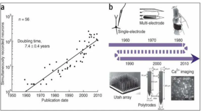
COMPARED WITH THE CELL BODY (50ΜM OR MORE).THE AXON TERMINALS OF THE PRESYNAPTIC NEURON TRANSMIT SIGNALS TO THE POSTSYNAPTIC CELLS (A). CONFIGURATION OF AN ACTION POTENTIAL:(B) PHASES OF AN ACTION POTENTIAL AND (C) INWARD AND OUTWARD CURRENT OF NA+ AND K+.[13] ... 2 FIGURE 1.2–EXPONENTIAL GROWTH IN THE NUMBER OF RECORDED NEURONS SEEN ON (A).THE NUMBER OF
SIMULTANEOUSLY RECORDED NEURONS DOUBLED APPROXIMATELY EVERY 7 YEARS;(B) SHOWS A TIMELINE OF RECORDING TECHNOLOGY DEVELOPMENT FROM SINGLE-ELECTRODE RECORDINGS TO MULTI-ELECTRODE ARRAYS AND IN VIVO IMAGING TECHNIQUES.[19] ... 3
FIGURE 1.3–GOUY-CHAPMAN-STERN MODEL OF THE ELECTROCHEMICAL DOUBLE LAYER (EDL).[27] ... 4
FIGURE 1.4–EQUIVALENT CIRCUIT OF A METAL MICROELECTRODE RECORDING FROM THE ISOPOTENTIAL LINE ‘EN’ OF A NEURON IN A CONDUCTOR VOLUME.[30] ... 4
FIGURE 1.5–OPTICAL MICROSCOSPE AND SEM IMAGES TAKEN OF MICROELECTRODES:(A) SILICON PROBE
(NEURONEXUS),(B) PRISTINE ELECTRODE,(C)AU:PVP COATED ELECTRODE AND (D)PEDOT:PSS
COATED ELECTRODE. ... 5
FIGURE 2.1–PICTURE FROM DIFFERENT SOLUTIONS PREPARED FOR ELECTRODEPOSITION.FROM LEFT TO RIGHT:EDOT:PSS, TUNGSTEN OXIDE NANOPARTICLES (WO3NPS), COMMERCIAL GOLD SOLUTION, AU:PVP SOLUTION, GOLD NANOPARTICLES SOLUTION, AND CARBON NANOTUBES SOLUTION. ... 8
FIGURE 2.2–PICTURE FROM THE NANOZ WITH THE TWO ELECTRODE CELL DEPOSITION SETUP (A).THE REFERENCE WIRE IS PLACED AROUND THE DEPOSITION CUP WHILE THE PROBE IS MAINTAINED AT A FIX AND EQUAL DISTANCE TO ALL POINTS OF THE REFERENCE WIRE (B). ... 10
FIGURE 3.1–AU NPS OBSERVED BY SEM:(A) SHOWS DISPERSED NANOPARTICLES AND (B) SHOWS THE PRESENCE OF BIG AGGLOMERATES OF NANOPARTICLES. ... 13
FIGURE 3.2–EDS SPECTRUM FOR AU NPS SAMPLES.PRESENCE OF AU NPS IS EVIDENT DUE TO THE GOLD PEAKS THROUGHOUT THE SPECTRUM. ... 14
FIGURE 3.3–WO3NPS OBSERVED ON SEM. ... 14 FIGURE 3.4-EDS SPECTRUM FOR WO3NPS SAMPLES.PRESENCE OF WO3NPS IS EVIDENT DUE TO THE GOLD
PEAKS THROUGHOUT THE SPECTRUM. ... 15
FIGURE 3.5 – XRD DIFFRACTOGRAMS OF: (A) WO3 SYNTHESIZED POWDER AND (B) ORTHORHOMBIC WO3.033H2O REFERENCE PATTERN (ICDD01-072-0199). ... 15 FIGURE 3.6-CNTS OBSERVED BY SEM:(A) SHOWS AN AGGLOMERATE OF CNTS WITH THEIR TYPICAL
CYLINDRICAL SHAPES AND (B) SHOWS THEIR HOLLOW STRUCTURE. ... 16 FIGURE 3.7-EDS SPECTRUM FOR CNT SAMPLES.PRESENCE OF C AND S INDICATE THAT CNTS AND SDS ARE
PRESENT ON THE SAMPLE ... 16
FIGURE 3.8-SURFACE MORPHOLOGY OF A PRISTINE ELECTRODE ON (A) AND A TYPICAL GOLD MODIFICATION ON (B),(C) AND (D). ... 17
FIGURE 3.9-ELECTROCHEMICAL CHARACTERIZATION OF NON-MODIFIED AND MODIFIED ELECTRODES (WITH COMMERCIAL GOLD SOLUTION):(A)EIS,(B) PHASE ANGLE,(C)NYQUIST PLOT AND (D)CV... 18
FIGURE 3.10 -SEM IMAGES FOR: (A) PRISTINE ELECTRODE,(B) MODIFIED WITH AU-PVP(-30 NA, 120
xviii
NANOSTRUCTURING SILICON PROBES VIA ELECTRODEPOSITION: CHARACTERIZATIONOF ELECTRODE COATINGS FOR ACUTE IN VIVO NEURAL RECORDINGS
FIGURE 3.11-ELECTROCHEMICAL CHARACTERIZATION OF NON-MODIFIED AND MODIFIED ELECTRODES WITH
AU-PVP SOLUTION:(A)EIS,(B) PHASE ANGLE,(C)NYQUIST PLOT AND (D)CV. ... 20
FIGURE 3.12-SEM IMAGES OF ELECTRODES COATED WITH AU NPS:(A) WELL DISTRIBUTED AMOUNT OF GOLD NANOPARTICLES AND (B) DENSE DISTRIBUTION OF AU NPS AT THE EDGE OF THE ELECTRODE. CONTAMINATION OUTSIDE THE ELECTRODE OBSERVED. ... 21
FIGURE 3.13-ELECTROCHEMICAL CHARACTERIZATION OF NON-MODIFIED AND MODIFIED ELECTRODES WITH
AU NPS:(A)EIS,(B) PHASE ANGLE,(C)NYQUIST PLOT AND (D)CV. ... 22
FIGURE 3.14–SEM IMAGES OF A PEDOT MODIFIED ELECTRODE WITH +30 NA FOR A PERIOD OF 5 SECONDS.
... 23
FIGURE 3.15-ELECTROCHEMICAL CHARACTERIZATION OF NON-MODIFIED AND MODIFIED ELECTRODES WITH
PEDOT/PSS:(A)EIS,(B) PHASE ANGLE,(C)NYQUIST PLOT AND (D)CV. ... 24
FIGURE 3.16–SEM IMAGES OF ELECTRODES MODIFIED WITH PEDOT AND AU NPS:(A)PEDOT:AU NPS COATED ELECTRODE AND (B) BACKSCATTERED ELECTRON IMAGE SHOWING GOLD NANOPARTICLES CLUSTERS ON TOP OF THE METAL LINES. ... 25
FIGURE 3.17 - ELECTROCHEMICAL CHARACTERIZATION OF NON-MODIFIED AND MODIFIED ELECTRODES
(WITH PEDOT:PSS AND AU NPS):(A)EIS,(B) PHASE ANGLE,(C)NYQUIST PLOT AND (D)CV. ... 25
FIGURE 3.18 - SCANNING ELECTRON MICROSCOPY (SEMFIB, ZEISS AURIGA) IMAGES OF ELECTRODES MODIFIED WITH PEDOT:CNT COMPOSITES:(A) PRISTINE ELECTRODE,(B),(C) AND (D)PEDOT:CNT
MODIFIED ELECTRODES WITH DIFFERENT CONCENTRATION OF CNTS:11%(V/V),20%(V/V) AND 47% (V/V), RESPECTIVELY.ELECTRODE AREA SHOWN IN RED. ... 26
FIGURE 3.19-ELECTROCHEMICAL CHARACTERIZATION OF NON-MODIFIED AND MODIFIED ELECTRODES WITH
PEDOT:CNT COMPOSITE:(A)EIS,(B) PHASE ANGLE,(C)NYQUIST PLOT AND (D)CV. ... 27
FIGURE 3.20-SEM IMAGES OF ELECTRODES COATED WITH WO3NPS:(A) DEPOSITED NEAR A METAL LINE
AND (B) DENSE DISTRIBUTION OF WO3NPS AT THE EDGE OF THE ELECTRODE. CONTAMINATION
OUTSIDE THE ELECTRODE OBSERVED. ... 28
FIGURE 3.21 - ELECTROCHEMICAL CHARACTERIZATION OF NON-MODIFIED AND MODIFIED ELECTRODES
(WITH WO3NPS):(A)EIS,(B) PHASE ANGLE,(C)NYQUIST PLOT AND (D)CV. ... 29 FIGURE 3.22 - ELECTRODE-COATING-ELECTROLYTE INTERFACE COMPONENTS SCHEME: (A) SHOWS THE
REPRESENTATION OF THE IMPEDANCE OF THE COATING-ELECTROLYTE INTERFACE AND (B) SHOWS THE EQUIVALENT CIRCUIT USED TO FIT THE IMPEDANCE SPECTRA. ... 29
FIGURE 3.23 – HIGH DENSITY 32 CHANNEL PROBE FROM NEURONEXUS: (A) SHOWS THE SITE NUMBER LAYOUT ON THE PROBE,(B) THE MODIFICATION LAYOUT WITH DIFFERENT MATERIALS AND (C) PROBE IMAGE WITH THE STANDARDS. ... 30
FIGURE 3.24–CELL ACTIVITY FROM MULTIPLE RECORDINGS TAKEN FROM THE TIP OF THE HDP.APPENDIX
SECTION G PRESENTS THE LOCATION OF THE RECORDINGS WITH THE CORRESPONDING BRAIN ATLAS MAP. ... 31
FIGURE 3.25–NEURAL SPONTANEOUS ACTIVITY WITHIN THE CORTEX FOR A PEDOT MODIFIED ELECTRODE: (A) HIGH-PASS FILTERED DATA CONTAINING 30 SECONDS OF INFORMATION,(B) ZOOM IN THE FILTERED DATA,(C) AND (D) SPIKE AVERAGE AND STANDARD DEVIATION OBTAINED AFTER APPLYING A VOLTAGE THRESHOLD (-100ΜV). ... 31
FIGURE 6.1–OPTICAL MICROSCOPE IMAGES TAKEN FOR MULTIPLE SILICON PROBE CONFIGURATIONS USED DURING THIS WORK. ... 39
xix
NANOSTRUCTURING SILICON PROBES VIA ELECTRODEPOSITION: CHARACTERIZATIONOF ELECTRODE COATINGS FOR ACUTE IN VIVO NEURAL RECORDINGS
FIGURE 6.3-IMPEDANCE DROP AFTER DEPOSITION FOR DIFFERENT COATING TIMES AND STABILITY AFTER ONE DAY
GIVEN BY IMPEDANCE RISING. ... 50
FIGURE 6.4-IMPEDANCE DROP AFTER DEPOSITION FOR DIFFERENT COATING TIMES AND STABILITY AFTER ONE DAY GIVEN BY IMPEDANCE RISING. ... 50
FIGURE 6.5-IMPEDANCE DROP AFTER DEPOSITION FOR DIFFERENT COATING TIMES AND STABILITY AFTER ONE DAY GIVEN BY IMPEDANCE RISING. ... 51
FIGURE 6.6-IMPEDANCE DROP AFTER DEPOSITION FOR DIFFERENT COATING TIMES AND STABILITY AFTER ONE DAY GIVEN BY IMPEDANCE RISING. ... 51
FIGURE 6.7 - IMPEDANCE DROP FOR PEDOT:CNT MODIFICATIONS AFTER DEPOSITION FOR DIFFERENT COATING CONCENTRATIONS AND STABILITY AFTER ONE DAY (GIVEN BY IMPEDANCE RISING). ... 52
FIGURE 6.8 -IMPEDANCE DROP FOR WO3 MODIFICATIONS AFTER DEPOSITION FOR DIFFERENT COATING
CONCENTRATIONS AND STABILITY AFTER ONE DAY (GIVEN BY IMPEDANCE RISING).NO DATA FOR 1
DAY AFTER DEPOSITION IS SHOWN THE IMPEDANCE RETURN TO ITS ORIGINAL VALUES. ... 52
FIGURE 6.9-ELECTROCHEMICAL IMPEDANCE SPECTROSCOPY SPECTRA GIVEN BY GAMRY ECHEM ANALYST
SOFTWARE.BODE PLOT ON (A) AND NIQUIST PLOT ON (B) FOR A PRISTINE ELECTRODE WITH THE RESPECTIVE DATA FITTING. ... 55
FIGURE 6.10 - ELECTROCHEMICAL IMPEDANCE SPECTROSCOPY SPECTRA GIVEN BY GAMRY ECHEM
ANALYST SOFTWARE. BODE PLOT ON (A) AND NIQUIST PLOT ON (B) FOR A COMMERCIAL GOLD SOLUTION COATING WITH THE RESPECTIVE DATA FITTING. ... 56
FIGURE 6.11 - ELECTROCHEMICAL IMPEDANCE SPECTROSCOPY SPECTRA GIVEN BY GAMRY ECHEM
ANALYST SOFTWARE. BODE PLOT ON (A) AND NIQUIST PLOT ON (B) FOR GOLD NANOPARTICLES COATING WITH THE RESPECTIVE DATA FITTING. ... 57
FIGURE 6.12 - ELECTROCHEMICAL IMPEDANCE SPECTROSCOPY SPECTRA GIVEN BY GAMRY ECHEM
ANALYST SOFTWARE.BODE PLOT ON (A) AND NIQUIST PLOT ON (B) FOR A PEDOT COATING WITH THE RESPECTIVE DATA FITTING. ... 58
FIGURE 6.13 - ELECTROCHEMICAL IMPEDANCE SPECTROSCOPY SPECTRA GIVEN BY GAMRY ECHEM
ANALYST SOFTWARE. BODE PLOT ON (A) AND NIQUIST PLOT ON (B) FOR A GOLD NANOFLAKES COATING WITH THE RESPECTIVE DATA FITTING. ... 59
FIGURE 6.14 - ELECTROCHEMICAL IMPEDANCE SPECTROSCOPY SPECTRA GIVEN BY GAMRY ECHEM
ANALYST SOFTWARE.BODE PLOT ON (A) AND NYQUIST PLOT ON (B) FOR A PEDOT:CNT COATING WITH THE RESPECTIVE DATA FITTING. ... 60
FIGURE 6.15 – ATLAS MAP OF THE RODENTS’ BRAIN WHERE THE PROBE WAS INSERTED (RED ARROW POINTING INSERTION REGION).INSERTION COORDINATES ARE AP(Y)3.24 MM,ML(X)1.75 MM AND
xx
NANOSTRUCTURING SILICON PROBES VIA ELECTRODEPOSITION: CHARACTERIZATIONxxi
NANOSTRUCTURING SILICON PROBES VIA ELECTRODEPOSITION: CHARACTERIZATIONOF ELECTRODE COATINGS FOR ACUTE IN VIVO NEURAL RECORDINGS Table Index
TABLE 3.1-AVERAGE DIAMETER AND STANDARD DEVIATION OBTAINED BY DLS AND SEM IMAGES FOR
AU NPS. ... 13
TABLE 3.2–EDS QUANTITATIVE ELEMENT ANALYSIS OF AVERAGE WEIGHT % AND AVERAGE ATOMIC %.
... 13
TABLE 3.3-AVERAGE DIAMETER AND STANDARD DEVIATION OBTAINED BY DLS AND SEM IMAGES FOR
WO3NPS. ... 14 TABLE 3.4-EDS ANALYSIS OF AVERAGE WEIGHT % AND AVERAGE ATOMIC %. ... 15
TABLE 3.5-EDS ANALYSIS OF AVERAGE WEIGHT % AND AVERAGE ATOMIC %. ... 16
TABLE 6.1-IMPEDANCE VALUES AND CHARGE STORAGE CAPACITY OBTAINED FOR GOLD DEPOSITIONS WITH DIFFERENT COATING TIMES. ... 49
TABLE 6.2–IMPEDANCE VALUES AND CHARGE STORAGE CAPACITY OBTAINED FOR GOLD NANOFLAKES DEPOSITIONS WITH DIFFERENT COATING TIMES. ... 49
TABLE 6.3–IMPEDANCE VALUES (AT 1004HZ) AND CHARGE STORAGE CAPACITY OBTAINED FOR GOLD DEPOSITIONS WITH DIFFERENT COATING TIMES. ... 50
TABLE 6.4–IMPEDANCE VALUES (AT 1004HZ) AND CHARGE STORAGE CAPACITY OBTAINED FOR GOLD DEPOSITIONS WITH DIFFERENT COATING TIMES. ... 50
TABLE 6.5-IMPEDANCE VALUES (AT 1004HZ) AND CHARGE STORAGE CAPACITY OBTAINED FOR GOLD DEPOSITIONS WITH DIFFERENT COATING TIMES. ... 51
TABLE 6.6-IMPEDANCE VALUES (AT 1004HZ) AND CHARGE STORAGE CAPACITY OBTAINED FOR GOLD DEPOSITIONS WITH DIFFERENT COATING TIMES. ... 51
TABLE 6.7-IMPEDANCE VALUES (AT 1004HZ) AND CHARGE STORAGE CAPACITY OBTAINED FOR GOLD DEPOSITIONS WITH DIFFERENT COATING TIMES. ... 52
TABLE 6.8–BEST RESULTS OBTAINED FOR DIFFERING ELECTRODE COATINGS. ... 53
TABLE 6.9-LIST OF ELEMENTS, CORRESPONDING SYMBOLS AND RELATIONS OF ADMITTANCE AND
IMPEDANCE. ... 54
TABLE 6.10-EQUIVALENT CIRCUIT PARAMETERS CALCULATED VIA GAMRY ECHEM ANALYST SOFTWARE FOR FITTING THE DATA FROM A PRISTINE ELECTRODE. ... 55
TABLE 6.11-EQUIVALENT CIRCUIT PARAMETERS CALCULATED VIA GAMRY ECHEM ANALYST SOFTWARE FOR FITTING THE DATA FROM AN ELECTRODE MODIFIED WITH A COMMERCIAL GOLD SOLUTION. ... 56
TABLE 6.12-EQUIVALENT CIRCUIT PARAMETERS CALCULATED VIA GAMRY ECHEM ANALYST SOFTWARE FOR FITTING THE DATA FROM AN ELECTRODE MODIFIED WITH GOLD NANOPARTICLES. ... 57
TABLE 6.13-EQUIVALENT CIRCUIT PARAMETERS CALCULATED VIA GAMRY ECHEM ANALYST SOFTWARE FOR FITTING THE DATA FROM AN ELECTRODE MODIFIED WITH PEDOT:PSS. ... 58
TABLE 6.14-EQUIVALENT CIRCUIT PARAMETERS CALCULATED VIA GAMRY ECHEM ANALYST SOFTWARE FOR FITTING THE DATA FROM AN ELECTRODE MODIFIED WITH GOLD NANOFLAKES. ... 59
TABLE 6.15-EQUIVALENT CIRCUIT PARAMETERS CALCULATED VIA GAMRY ECHEM ANALYST SOFTWARE FOR FITTING THE DATA FROM AN ELECTRODE MODIFIED WITH A SOLUTION OF PEDOT AND CARBON
NANOTUBES. ... 60
TABLE 6.16–ACUTE NEURAL EXPERIMENT DATA FROM DIFFERENT RECORDINGS. ... 61
TABLE 6.17–ELECTRODEPOSITION PARAMETERS USED FOR COATINGS WITH DIFFERENT MATERIALS. ... 62
xxii
NANOSTRUCTURING SILICON PROBES VIA ELECTRODEPOSITION: CHARACTERIZATIONxxiii
NANOSTRUCTURING SILICON PROBES VIA ELECTRODEPOSITION: CHARACTERIZATION1
NANOSTRUCTURING SILICON PROBES VIA ELECTRODEPOSITION: CHARACTERIZATIONOF ELECTRODE COATINGS FOR ACUTE IN VIVO NEURAL RECORDINGS
1.
Introduction
1.1. Overview
Steady progress in biology and medicine has led to major advances in our comprehension of how complex living systems function. However, one of the ultimate challenges facing science and engineering remains – understanding how the brain works. Developing a theory explaining brain functionality would not only be a major advance in the field of biology, but it would also open paths allowing the comprehension of the pathophysiology of neurological and neuropsychi-atric diseases such as Alzheimer’s, Parkinson’s, Amyotrophic Lateral Sclerosis (ALS), Dementia and Epilepsy. [1] But even with the enormous efforts and substantial progress made by neurosci-entists trying to comprehend the molecular and cellular components of neural circuits both in humans and in animals, an all-encompassing theory explaining how the brain works is yet to be found. [2]
Hence, continued progress in neuroscience is vital yet with approximately eighty-five bil-lion neurons, one hundred trilbil-lion synapses and over one hundred chemical neurotransmitters in the human brain, this is an overwhelming task. Communication between neurons is the cellular basis for thinking, decision making and control of muscular movement. [3]
Neurons are specialized cells that input, process, store and output information through elec-trical and chemical signals in four basic paths: (i) Ca2+ evoked exocytosis with chemical neuro-transmission, (ii) gap junction electronic coupling, (iii) secretion of neurosteroids, nitric oxide and derivatives of the arachidonic acid acting in paracrine manner, and (iv) cellular adhesive protein interaction with scaffold protein reorganization. [4] At rest, the neuron’s cell membrane has an excess of positive charges at the extracellular surface, and the cytoplasm an excess of negative charge. The charge separation gives rise to a voltage across the membrane called mem-brane potential [5]. Temporary changes in the current flow into and out of the cell produce elec-trical signals that drive a potential across the cell membrane – action potential (Figure 1.1). These produce a large transmembrane voltage change due to the ionic movement across the membrane through voltage-gated channels in the vicinity of the soma (axon hillock) that can be detected in the extracellular environment by placing a conductor in close proximity to the neuron. The elec-trodes record a combined extracellular signal gathered from all the spiking neurons in its vicinity and the contribution of a single neuron depends on its distance to the electrode. [6, 7]
2
NANOSTRUCTURING SILICON PROBES VIA ELECTRODEPOSITION: CHARACTERIZATIONOF ELECTRODE COATINGS FOR ACUTE IN VIVO NEURAL RECORDINGS
understanding of neural network behavior, drug discovery pharmacology and cell-based biosen-sors. [8] In one hand, the use of non-invasive tools allows whole brain imaging through different available techniques (electroencephalography (EEG), positron emission tomography (PET) and functional magnetic resonance imaging (fMRI)) that span the scale of both spatial and temporal resolution. [9] On the other hand, by using invasive techniques it’s possible to visualize popul a-tions and networks of neurons. [10,11,12]
Figure 1.1 – The structure of a neuron. Axons are the transmitting element of neurons: Most axons in the central
nervous system are very thin (between 0.2 and 20 μm in diameter) compared with the cell body (50 μm or more).
The axon terminals of the presynaptic neuron transmit signals to the postsynaptic cells (a). Configuration of an action potential: (b) phases of an action potential and (c) inward and outward current of Na+ and K+. [13]
Therefore, the use of invasive tools to record the electrical brain activity has led to sig-nificant advances in basic neuroscience. [14] In the past, neuroscience research focused on the recording of single neurons due to their available tools (single wires for example). However, the need of retrieving information from complex neuron networks has led to the creation of new systems such as arrays of wires, silicon shafts and other complex micro machined silicon systems; all of these with a capability for probing simultaneously more individual neurons. [15]
3
NANOSTRUCTURING SILICON PROBES VIA ELECTRODEPOSITION: CHARACTERIZATIONOF ELECTRODE COATINGS FOR ACUTE IN VIVO NEURAL RECORDINGS
Figure 1.2 – Exponential growth in the number of recorded neurons seen on (a). The number of simultaneously recorded neurons doubled approximately every 7 years; (b) shows a timeline of recording technology develop-ment from single-electrode recordings to multi-electrode arrays and in vivo imaging techniques. [19]
As shown in Figure 1.2, the development from single-electrode recordings to multi-elec-trode arrays and in vivo imaging techniques has increased the number of simultaneously recorded neurons. Optical imaging of multiple single neurons is a recent promising development in this field. However, this approach is too slow to monitor action potentials and is not practical for monitoring deep cortical activity. [20] To achieve high spatial resolution of neural recording with extracellular probes, efforts are underway to produce ultra-high density probes with small elec-trodes (< 10 μm) arranged in dense arrays. [21] Micro and nanosystems technology allow for the arrangement of multiple microelectrodes on the same substrate over small distances. Thus, there is a possibility for simultaneous recording from many neurons. However, to accomplish this task, and in order to optimize the recorded data and allow identification of all adjacent neurons, a high quality signal from the nearby tissue must be obtained. [22, 23] With current electrodes, there are problems and fundamental limits for the current materials used in respect to charge storage ca-pacity and impedance. Therefore, it is desired to develop microelectrodes for simultaneous mon-itoring of neural activity from multiple neurons in order to record in vivo neural activity from the largest number of neurons possible distributed in different places throughout the brain. [24] Im-proving existing tools, as proposed in this thesis, promotes a connection between neuroscience and nanotechnology and allow both the possibility of mapping neuronal circuits and to compre-hend brain functionality. [25]
1.2. Electrode-tissue interface
4
NANOSTRUCTURING SILICON PROBES VIA ELECTRODEPOSITION: CHARACTERIZATIONOF ELECTRODE COATINGS FOR ACUTE IN VIVO NEURAL RECORDINGS
Figure 1.3 – Gouy-Chapman-Stern model of the Electrochemical Double Layer (EDL). [27]
The exact nature of this charge distribution depends on the conductor material, the surface properties of the microelectrode, as well as on the amplitude and frequency of the electrical sig-nals involved, and is the key for understanding the signal transduction across the electrode-tissue interface. [22]
1.3. Electrode modifications
For recording electrodes, different materials have been used such as platinum, gold, tung-sten, iridium and even stainless steel taking usually in consideration the impedance magnitude at 1 kHz (biological relevant frequency of a neural action potential). [28, 29]
Figure 1.4 – Equivalent circuit of a metal microelectrode recording from the isopotential line ‘en’ of a neuron in a conductor volume. [30]
Metal electrode-tissue interface can be represented by a parallel ReCe combination in se-ries with the resistances, Rm and RS, due to the metal interconnects and the solution, respectively. The frequency-dependent impedance Z (jω), where j is the imaginary number and ω is the angular frequency.
𝑍 (𝑗𝜔) = 𝑍′+ 𝑗𝑍′′ = 𝑅
𝑠+1 + (𝜔𝑅𝑅𝑒
𝑒𝐶𝑒)2− 𝑗
𝜔𝑅𝑒2𝐶𝑒 1 + (𝜔𝑅𝑒𝐶𝑒)2
Where Rs = RS + Rmis the lumped series resistance, and Z’ and Z’’ are the real (resistance) and imaginary (reactance) part of the impedance. For recording electrodes, the impedance magnitude
5
NANOSTRUCTURING SILICON PROBES VIA ELECTRODEPOSITION: CHARACTERIZATIONOF ELECTRODE COATINGS FOR ACUTE IN VIVO NEURAL RECORDINGS
at 1 kHz is very important since this is the characteristic frequency of a neural action potential (1 ms). For such a high frequency, Eq. 1.1 can be approximated by:
𝑍 (𝑗𝜔) = 𝑅𝑠+ 𝑗𝜔𝐶1 𝑒
Since Rs<< (1/ωCe) we obtain:
|𝑍|(𝜔) ≈𝜔𝐶1 𝑒
Taking in consideration the Guy-Chapman-Stern theory, the electrodes capacitance is given by Equation 1.4 where CHis the Helmholtz capacitance, ε0 the vacuum permittivity, εr the dielectric constant, A the electrodes area and dOHP the distance to the Outer Helmholtz Plane (Figure 1.3). Since impedance scales inversely with the capacitance, miniaturizing the electrodes area (for the design of probes with multiple micro and nanoelectrodes) would increase their impedance. [31]
𝐶𝐻=𝜀𝑑0𝜀𝑟𝐴 𝑂𝐻𝑃
The design of these small electrodes that are biocompatible, highly conductive, with a high tough-ness, long-term resilience to the biological environment and with the desired impedance values depends on new approaches concerning their fabrication. [32] Conventional materials used to make these electrodes do not provide significantly low impedance at such scales. Therefore, there’s a need in modifying these electrodes either by replacing the pristine material or by coating them with nanostructures or porous materials leading to lower impedance values and a wide range of new properties such as improved conductivity or increase charge storage capacity. [31]
Figure 1.5 – Optical microscospe and SEM images taken of microelectrodes: (a) silicon probe (Neuronexus), (b) pristine electrode, (c) Au:PVP coated electrode and (d) PEDOT:PSS coated electrode.
Eq. 1.2
Eq. 1.3
Eq. 1.4
(a) (b)
6
NANOSTRUCTURING SILICON PROBES VIA ELECTRODEPOSITION: CHARACTERIZATION7
NANOSTRUCTURING SILICON PROBES VIA ELECTRODEPOSITION: CHARACTERIZATIONOF ELECTRODE COATINGS FOR ACUTE IN VIVO NEURAL RECORDINGS
2.
Materials and Methods
The work abridged in this dissertation involved the synthesis and characterizations of a broad range of solutions and their electrodeposition on silicon probe’s electrodes. Following the electrodeposition, electrochemical and morphological characterizations were performed. To con-clude the work, neural recordings of spontaneous activity within the motor cortex were performed in anesthetized rodents to evaluate the performance of the electrode’s coatings. This chapter sum-marizes relevant techniques used.
2.1. Solution-based synthesis
2.2.1. Commercial gold solution
Commercial non-cyanide gold solution was obtained from Neuralynx.
2.1.2. Tetrachloroauric acid solution (HAuCl4) – Polyvinylpyrrolidone (PVP)
Gold solution synthesis was obtained by mixing a 25 mM tetrachloroauric acid solution (Sigma-Aldrich, 99.9%) with polyvinylpyrrolidone (20% (w/v); Sigma-(Sigma-Aldrich, MW = 10 000). [33]
2.1.3. Gold nanoparticles (Au NPs)
Synthesis of gold nanoparticles was done via the citrate reduction method. A solution consisting of 1 mM of tetrachloroauric acid (Sigma-Aldrich, 99.9%) was heated on a hot plate with a mag-netic stirrer until it reached the boiling point. To this solution, 1% (w/v) trisodium citrate (AnalaR NORMAPUR, 100%) was added quickly and continuously stired. After the addition of the so-dium citrate solution, stirring continued until the solution turned red. [34]
2.1.4. Poly(3,4-ethylenedioxythiophene) – Poly(styrenesulfonate) (PEDOT:PSS)
Initial preparation of EDOT:PSS is achieved by mixing 0.01 M of EDOT (Sigma-Aldrich, 97%, MW = 142.18) in water and adding 0.1 M of PSS (Sigma-Aldrich, MW = 1000000). The solution must be vigorously stirred to dissolve the EDOT. PEDOT:PSS is obtained after the polymeriza-tion process during electrodeposipolymeriza-tion.
2.1.5. Tungsten oxide nanoparticles (WO3 NPs)
8
NANOSTRUCTURING SILICON PROBES VIA ELECTRODEPOSITION: CHARACTERIZATIONOF ELECTRODE COATINGS FOR ACUTE IN VIVO NEURAL RECORDINGS 2.1.6. Carbon Nanotubes – Sodium dodecyl Sulfate (CNTs:SDS)
For the preparation of the carbon nanotubes solution, 1.6 mg of CNTs (Multi-Wall (MW) CNTs, NANOCYLTM) were added to a solution containing 0.3% (w/v) SDS (Sigma-Aldrich, 98.5%). The solution was then submitted to 45 minutes of an ultrasonic bath (Bandelin Sonorex) followed by sonication (Sonics VibraCell) for a period of 2 minutes. The final solution product was then collected by centrifugation at 4000 rpm for 90 minutes (Focus Instruments). [36]
2.1.7. Carbon Nanotubes – Poly(3,4-ethylenedioxythiophene) composite (CNTs:PEDOT)
Composite mixtures of carbon nanotubes with PEDOT:PSS were obtained by mixing the previous CNTs:SDS solution with EDOT:PSS solution at three different volume ratios, respectively: 11% (v/v), 20% (v/v) and 50% (v/v). PEDOT:PSS is obtained after the polymerization process during electrodeposition.
2.1.8. Gold Nanoparticles - Poly(3,4-ethylenedioxythiophene) composite (Au NPs:PEDOT)
Composite mixtures of gold nanoparticles with EDOT:PSS were obtained by mixing the previous gold nanoparticle solution with EDOT:PSS solution at three different volume ratios respectively: 11% (v/v), 20% (v/v) and 47% (v/v). PEDOT:PSS is obtained after the polymerization process during electrodeposition.
After the synthesis all solutions were stored at low temperatures (4 - 6 ºC) in order to prevent deterioration. Later the solutions were used for electrodeposition at room temperature.
Figure 2.1 – Picture from different solutions prepared for electrodeposition. From left to right: EDOT:PSS, tungsten oxide nanoparticles (WO3 NPs), commercial gold solution, Au:PVP solution, gold nanoparticles
solu-tion, and carbon nanotubes solution.
2.2. Solution Characterization
2.2.1. X-Ray Diffracion (XRD)
Structural characterization of tungsten oxide powder was performed by X-ray diffraction (XPert PRO, PANalytical).
2.2.1. Dynamic Light scattering (DLS)
9
NANOSTRUCTURING SILICON PROBES VIA ELECTRODEPOSITION: CHARACTERIZATIONOF ELECTRODE COATINGS FOR ACUTE IN VIVO NEURAL RECORDINGS 2.2.3. Scanning Electron Microscopy (SEM)
Gold and tungsten oxide nanoparticles morphology and size were confirmed by scanning electron microscopy (SEM-FIB, Zeiss Auriga).
2.2.4. Energy-dispersive X-ray Spectroscopy (EDS)
Elemental analysis and chemical characterization of the electrode coatings was performed by en-ergy-dispersive x-ray spectroscopy (SEM-FIB, Zeiss Auriga).
2.3. Silicon Probes
Silicon probes (polytrodes from Neuronexus) with different configurations were used (Appendix Section A):
- One shank: 16 electrodes with a diameter of 30 μm; - One shank: 32 electrodes with a diameter of 15 μm;
- Two shank: 8 electrodes per shank presenting a tetrode configuration - in total 16 electrodes with a diameter of 20 μm;
- Four shank: 8 electrodes per shank presenting a tetrode configuration - in total 32 electrodes with a diameter of 20 μm;
- Eight shank: 4 electrodes per shank presenting a tetrode configuration - in total 32 electrodes with a diameter of 20 μm.
2.3.1. Silicon probe characterization
Prior to surgery, all electrode arrays were evaluated in terms of morphological and electrochem-ical performance.
2.3.2. Electrochemical characterization
A Gamry Instruments Potentiostat (Gamry Instruments, Reference 3000) was used with a three electrode cell configuration where the silicon probe’s electrodes were connect as the working electrodes, a platinum wire served as counter electrode and an Ag/AgCl wire as the reference electrode. Every microelectrode was characterized in a phosphate buffered saline solution (PBS 1x) by electrochemical impedance spectroscopy (EIS) (1 MHz to 1 Hz) and cyclic voltammetry (CV) (voltage range from -0.2 to 0.8 V, ν = 0.1 V s-1). The fitting of the impedance spectra was carried out using Gamry Echem Analyst software by testing different models for each solution. All electrochemical data was then compared to pristine (non-modified) microelectrodes and also between different coatings. Moreover, NanoZ (Neuralynx) was used to measure impedance at 1 kHz with a two electrode cell configuration – probes were connected as working electrodes and the reference electrode was an Ag/AgCL wire (Science Products GmbH, E-255).
2.3.3. Morphological characterization
10
NANOSTRUCTURING SILICON PROBES VIA ELECTRODEPOSITION: CHARACTERIZATIONOF ELECTRODE COATINGS FOR ACUTE IN VIVO NEURAL RECORDINGS 2.3.4. Electrodeposition set-up
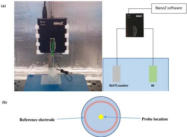
The electrochemical depositions were done with the NanoZ hardware through a galvanostatic deposition process (constant current and varied time). Moreover, NanoZ was used with a two electrode cell configuration as shown in Figure 2.2.
Figure 2.2 – Picture from the NanoZ with the two electrode cell deposition setup (a). The reference wire is placed around the deposition cup while the probe is maintained at a fix and equal distance to all points of the reference wire (b).
By using the ‘Manual Control’ from the software it’s possible to select individual probe elec-trodes. For each probe, an electrode array map must be created. Deposition process starts after selecting the deposition current.
2.4. Acute Recordings
For in vivo experiments we utilize anesthetized rodents (Long Evans) that are head-stabilized in
a stereotaxic frame and receiving intraperitoneal injections to maintain an adequate depth of an-esthesia during the surgery (Ketamine and Medetomidine, respectively, 1 g/10 mL and 1 mg/ml). Equipment for monitoring animal health (body temperate) as well as a video system for dorsal craniotomy and durotomy were integrated into the setup.
Anesthetized rodents undergo a surgical procedure to remove the skin and expose the skull above the targeted brain regions. An image of the exposed skull is acquired. Landmarks on the skull are then identified and used to target the brain region of interest with the help of a rat brain atlas in stereotaxic coordinates. [37] A craniotomy (4 x 2 mm) was made above the targeted brain region
Reference electrode Probe location
(a)
11
NANOSTRUCTURING SILICON PROBES VIA ELECTRODEPOSITION: CHARACTERIZATIONOF ELECTRODE COATINGS FOR ACUTE IN VIVO NEURAL RECORDINGS
and the dura matter was removed to expose the brain surface where the brain vasculature, is vis-ible. It was possible to evaluate the superficial damage that occurs during the probe insertion/ex-traction.
The high density electrode array silicon (Poly3-25s, Neuronexus Technologies) was then inserted to target the layer 5 of cortex. The silicon probe is on a micromanipulator that was lowered at a constant velocity (1 –5 μm s-1). Spontaneously neural activity was recorded from each electrode site available on the probe (32 electrodes). An open-source electrophysiology acquisition board (Open Ephys) was used along with a RDH2000 series digital electrophysiology interface chip that filter, amplify, and multiplex 32 channels (Intan Technologies). Electrodes are connected to one side of the chip, and digital data streams out the other side after analog-to-digital conversion with 16-bit resolution. The acquisition of extracellular traces sampled at 30 kSamples/s in a fre-quency band from 0.1 to 7500 Hz was performed for subsequent offline analysis.
12
NANOSTRUCTURING SILICON PROBES VIA ELECTRODEPOSITION: CHARACTERIZATION13
NANOSTRUCTURING SILICON PROBES VIA ELECTRODEPOSITION: CHARACTERIZATIONOF ELECTRODE COATINGS FOR ACUTE IN VIVO NEURAL RECORDINGS
3.
Results
3.1. Solution characterization 3.1.1. Au NPs
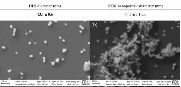
Au NPs morphology was evaluated via SEM. Even though some agglomerates can be seen (Figure 3.1), the nanoparticles have a spherical shape with an average diameter value close to 15 nm (14.5 ± 3.1 nm), corresponding to what is obtained through this technique in literature. [34] Additionally, by Dynamic Light Scattering (DLS), the nanoparticles dispersion was charac-terized with a mean hydrodynamic diameter of 13.1 ± 0.6 nm which is in accordance with SEM images.
Table 3.1 - Average diameter and standard deviation obtained by DLS and SEM images for Au NPs.
DLS diameter (nm) SEM nanoparticle diameter (nm)
13.1 ± 0.6 14.5 ± 3.1 nm
Figure 3.1 – Au NPs observed by SEM: (a) shows dispersed nanoparticles and (b) shows the presence of big agglomerates of nanoparticles.
A chemical analysis of the produced nanoparticles was performed by EDS to determine the syn-thesis quality. Table 3.2 and Figure 3.2 show the presence of gold (Au) corresponding to the nanoparticles and also to other chemical elements. Silicon (Si) and oxygen (O) are present due to the presence of the silicon wafer, and sodium (Na) and chlorine (Cl) appear due to the use of sodium citrate (Na3C6H5O7) and gold salts (HAuCl4) during the nanoparticle synthesis.
Table 3.2 – EDS quantitative element analysis of average weight % and average atomic %.
Average Weight % Average Atomic %
O K 10.84 22.43
Na K 2.78 4.05
Si K 57.55 67.65
Cl K 1.24 1.17
(a)
14
NANOSTRUCTURING SILICON PROBES VIA ELECTRODEPOSITION: CHARACTERIZATIONOF ELECTRODE COATINGS FOR ACUTE IN VIVO NEURAL RECORDINGS
Au M 27.59 4.70
Figure 3.2 – EDS spectrum for Au NPs samples. Presence of Au NPs is evident due to the gold peaks through-out the spectrum.
3.1.2. Tungsten Oxide Nanoparticles (WO3 NPs)
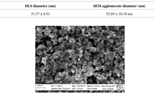
For the WO3 NPs, the hydrothermal synthesis was chosen due to the low manufacture temperatures, easy morphologic and structural control of the nanoparticles and good reproduci-bility. [35] The morphology of WO3 NPs was obtained via SEM. The nanoparticles present a non-uniform shape and are largely agglomerated to each other. The average diameter values obtained are close to 53 nm (52.69 ± 10.10 nm), corresponding to what is described in literature. [35] Also by DLS, the nanoparticle dispersion was characterized with a mean hydrodynamic diameter of 51.57 ± 6.91 nm which is in accordance with SEM images (Figure 3.3).
Table 3.3 - Average diameter and standard deviation obtained by DLS and SEM images for WO3 NPs.
DLS diameter (nm) SEM agglomerate diameter (nm)
51.57 ± 6.91 52.69 ± 10.10 nm
15
NANOSTRUCTURING SILICON PROBES VIA ELECTRODEPOSITION: CHARACTERIZATIONOF ELECTRODE COATINGS FOR ACUTE IN VIVO NEURAL RECORDINGS
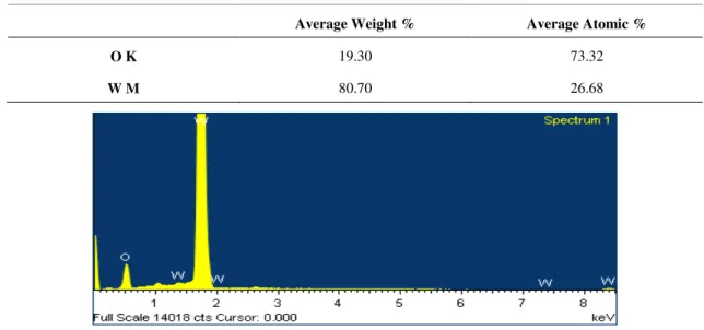
The analysis of the chemical composition of the nanoparticles was obtained by EDS. Table 3.4 and Figure 3.4 show the presence of high amounts of tungsten (W) corresponding to the nanoparticles. Other chemical elements were also detected (Si, K, Na and Cl) due to reasons already specified above.
Table 3.4 - EDS analysis of average weight % and average atomic %.
Average Weight % Average Atomic %
O K 19.30 73.32
W M 80.70 26.68
Figure 3.4 - EDS spectrum for WO3 NPs samples. Presence of WO3 NPs is evident due to the gold peaks
throughout the spectrum.
The crystallographic structure obtained for these nanoparticles was characterized by XRD (Figure 3.5). The structure obtained can be attributed to orthorhombic hydrated tungsten oxide (ortho-WO3.0.33H2O). All diffraction peaks can be indexed to the reference pattern ICDD 01-072-0199, except in the case of the marked peaks which are probably due to structure distor-tion caused by the lack of total formadistor-tion of the nanoparticles. This leads to a wide range of nanoparticle sizes and broad XRD peaks which are typical for structures with low crystallinity or nanocrystallinity. [35]
Figure 3.5 – XRD diffractograms of: (a) WO3 synthesized powder and (b) orthorhombic WO3.033H2O reference
16
NANOSTRUCTURING SILICON PROBES VIA ELECTRODEPOSITION: CHARACTERIZATIONOF ELECTRODE COATINGS FOR ACUTE IN VIVO NEURAL RECORDINGS 3.1.3. CNTs
The morphology of the CNTs was evaluated via SEM. Hollow cylindrical shaped CNTs were observed and can be seen in Figure 3.6. The average diameter values obtained by SEM are close to 11 nm (11.08 ± 1.65 nm).
Figure 3.6 - CNTs observed by SEM: (a) shows an agglomerate of CNTs with their typical cylindrical shapes and (b) shows their hollow structure.
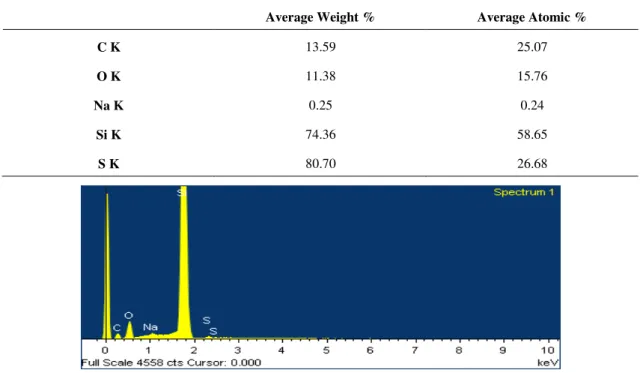
The analysis of the chemical composition of the CNTs was obtained by EDS. Table 3.5 and Figure 3.7 show the presence of high amounts of carbon (C) corresponding to the CNTs. Other chemical elements were also detected, with sulphur (S) and sodium (Na) being the result of the use of sodium dodecyl sulfate (SDS: CH3(CH2)11OSO3Na) as a dispersing agent for the CNTs.
Table 3.5 - EDS analysis of average weight % and average atomic %.
Average Weight % Average Atomic %
C K 13.59 25.07
O K 11.38 15.76
Na K 0.25 0.24
Si K 74.36 58.65
S K 80.70 26.68
17
NANOSTRUCTURING SILICON PROBES VIA ELECTRODEPOSITION: CHARACTERIZATIONOF ELECTRODE COATINGS FOR ACUTE IN VIVO NEURAL RECORDINGS 3.2. Coating characterization
Different parameters were used in order to ascertain which would be the optimal modifi-cation to be used on the silicon probes’ electrodes with the diameters presented on the previous chapter. It’s known that a low deposition current would yield a poor modification of the electrode and a high deposition current value could lead to a contamination outside the electrode (conse-quently lead to short-circuit between them). Moreover, the impedance drop, stability over time (normally a period of a few days/to a week) and low material contamination outside the electrodes were taken into consideration.
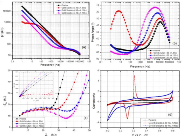
3.2.1. Commercial Gold Solution
Commercial gold solution has been used as the standard material for coating electrodes. [38] During this work, gold deposition parameters will be assessed for future reference in order to optimize the coating process.
Figure 3.8 - Surface morphology of a pristine electrode on (a) and a typical gold modification on (b), (c) and (d).
Figure 3.8 shows the morphological differences between a pristine electrode and a gold coated electrode. A smooth surface is observed on Figure 3.8 (a) (pristine electrode) while a more rough surface is seen on Figure 3.8 (b) (gold coated electrode). This increase in surface area is one of the key aspects in lowering the impedance modulus at 1 kHz (frequency for neurons ac-tivity, action potential). The results presented on Figure 3.9 for gold coated electrodes (commer-cial gold solution) show a change in impedance (lower impedance values by increasing deposition times) and charge storage capacity (higher charge storage capacity by increasing deposition
(a)
(b)
18
NANOSTRUCTURING SILICON PROBES VIA ELECTRODEPOSITION: CHARACTERIZATIONOF ELECTRODE COATINGS FOR ACUTE IN VIVO NEURAL RECORDINGS
times). Different behaviors/ electrochemical performances were observed for the different depo-sition times which will be discussed in detail.
Figure 3.9 - Electrochemical characterization of non-modified and modified electrodes (with commercial gold solution): (a) EIS, (b) phase angle, (c) Nyquist plot and (d) CV.
19
NANOSTRUCTURING SILICON PROBES VIA ELECTRODEPOSITION: CHARACTERIZATIONOF ELECTRODE COATINGS FOR ACUTE IN VIVO NEURAL RECORDINGS
iridium electrodes) means that depositions below 90 seconds aren’t ideal for coating these elec-trodes. The response given at 1004 Hz shows that an electrode coating with a 180 second depo-sition (-30 nA) yields a lower impedance value. Though this may seem as the ideal parameters to obtain a higher impedance drop, a higher structural instability is attained meaning that the struc-tures formed on top of the electrodes tend to deteriorate in a short period of time leading to an increase in the impedance value.
The electrochemical stability of these gold coatings was evaluated by CV (cycle number 3 was used in total of 7 cycles) and a higher overall capacity was achieved for depositions with higher times. The highest capacity obtained (total area under the CV curve calculated on Echem Gamry Analyst) was 6.65 mC/cm2 (11.7 nF) for a 180 second deposition which corresponds to approximately 3 times the capacity of a pristine electrode. The characteristic redox peaks indi-cating the presence of gold on the electrodes are seen at approximately 50 mV and 200 mV. [39] The data presented on Table 6.1 and Figure 6.2 (Appendix Section C) shows the variation in impedance before and after deposition, also taking in consideration the impedance values one day after deposition in order to assess stability of the coatings and, charge storage capacity for each coating.
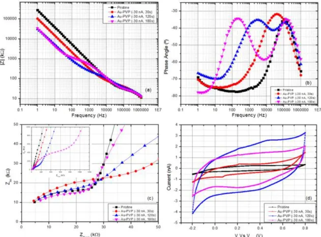
3.2.2. Au-PVP
Figure 3.10 - SEM images for: (a) pristine electrode, (b) modified with Au-PVP (-30 nA, 120 seconds) and (c) modified with Au-PVP (-30 nA, 180 seconds).
The optimal parameters obtained for the Gold-PVP solution were -30 nA during a con-tinuous deposition of 120 seconds. A lower deposition time (30 seconds) wouldn’t be enough for
(a)
(b)
20
NANOSTRUCTURING SILICON PROBES VIA ELECTRODEPOSITION: CHARACTERIZATIONOF ELECTRODE COATINGS FOR ACUTE IN VIVO NEURAL RECORDINGS
the formation of nanostructures and for the complete coverage of the electrode. A higher deposi-tion time (180 seconds) would yield in the agglomeradeposi-tion of gold disenabling the formadeposi-tion of nanostructure (Figure 3.10). Also, longer deposition times create a structure that stretches beyond the limits of the electrodes area which demonstrates to be highly unstable since, after one day, the electrodes impedance returns to its initial value. Moreover, the acidity of the solution (pH value of 2.5) for higher deposition times can lead to unwanted damage influencing the electrodes im-pedance. The morphological differences between the pristine electrode and the Au-PVP coated electrodes can be cleared observed on Figure 3.10 with a highly rough structure due to the nanostructures formed on top of the electrodes (highest increased surface area observed on Figure 3.10 (b) for a 120 second deposition).
Figure 3.11 - Electrochemical characterization of non-modified and modified electrodes with Au-PVP solution: (a) EIS, (b) phase angle, (c) Nyquist plot and (d) CV.
21
NANOSTRUCTURING SILICON PROBES VIA ELECTRODEPOSITION: CHARACTERIZATIONOF ELECTRODE COATINGS FOR ACUTE IN VIVO NEURAL RECORDINGS
KHz and 200 Hz, respectively). These can also be seen in the Nyquist plots (Figure 3.11 (c)) by the display of two semi-circles.
The second peak (second time constant) may be linked with the external and porous layer formed by the Au-PVP coating. [40] Electrodes coated with the optimal parameters described previously, showed a better stability and higher overall capacity when compared to a pristine and commercial gold modified electrode. The highest charge storage capacity obtained was 19.46 mC/cm2 (34.4 nF) for a 120 second deposition which represents approximately 9 times the capac-ity of a pristine electrode. The characteristic redox peaks indicating the presence of gold on the electrodes are seen at approximately 50 mV and 200 mV. The data presented on Table 6.2 and Figure 6.3 (Appendix Section C) shows the variation in impedance obtained before and after deposition, also taking in consideration the impedance values one day after deposition in order to assess stability of the coatings) and charge storage capacity for each coating.
3.2.3. Au NPs
Due to their small size (around 15 nm), gold nanoparticles are expected to yield a rugged nanostructure on top of the electrodes increasing total surface area. Several parameters were used, modifying both current and time as well as type of deposition (pulsed or continuous deposition). It was found in one hand that continuous depositions below 10 seconds resulted in low or virtually no deposition on top of the electrodes and in another hand high deposition times (above 120 seconds) would contaminate the entire probe. Therefore, small pulsed depositions were used in order to avoid the contamination. Also, the amount of nanoparticles deposited on top of the trodes was rather small but there was a uniform distribution of nanoparticles on top of the elec-trodes. This way, it was possible to avoid aggregation of nanoparticles. [41,42] Morphologically, the gold nanoparticles tend to aggregate in a coral like structure on top of the electrodes increasing the total surface area.
Figure 3.12 -SEM images of electrodes coated with Au NPs: (a) well distributed amount of gold nanoparticles and (b) dense distribution of Au NPs at the edge of the electrode. Contamination outside the electrode observed.
Outside of the electrode Electrode
22
NANOSTRUCTURING SILICON PROBES VIA ELECTRODEPOSITION: CHARACTERIZATIONOF ELECTRODE COATINGS FOR ACUTE IN VIVO NEURAL RECORDINGS
The results showed that throughout the frequency range, gold nanoparticle coated elec-trodes displayed a slight decrease on the impedance modulus (Figure 3.13 (a)) and an increase on the charge storage capacity (Figure 3.13 (d)).
Figure 3.13 - Electrochemical characterization of non-modified and modified electrodes with Au NPs: (a) EIS, (b) phase angle, (c) Nyquist plot and (d) CV.
23
NANOSTRUCTURING SILICON PROBES VIA ELECTRODEPOSITION: CHARACTERIZATIONOF ELECTRODE COATINGS FOR ACUTE IN VIVO NEURAL RECORDINGS 3.2.4. PEDOT:PSS
Conducting polymers have been the focus of extensive studies and due to their electronic and ionic conductivity, they provide low impedance and high storage charge capacitance. [45] In addition, these materials are complemented with pseudocapacitance due to redox reactions and chemisorption processes that take place at the electrode surfaces of conducting polymers. Im-portantly, this kind of capacitance is faradaic in nature, rather than being associated with poten-tial-dependent accumulation of electrostatic charge. [27]
Figure 3.14 – SEM images of a PEDOT modified electrode with +30 nA for a period of 5 seconds.
Figure 3.14 shows a trans-lucid coating on top of the electrodes. Compared to metals, these conducting polymer coatings presented a relatively soft material when coated onto the elec-trodes surface. With the NanoZ equipment, under galvanostatic conditions, the working potential usually starts at values above +1.0 V and rapidly decreases (almost instantaneously) indicating a decline in the impedance modulus. The parameters used to provide the best coating are +30 nA for a 5 second deposition. With a deposition time of 15 seconds, there is a high probability of short circuiting nearby electrodes in these high density probes since the coating area is broader than the electrode area. So, with increased deposition time, the outgrowth of PEDOT is a factor to be taken under consideration. By lowering the deposition time to 5 seconds, it’s possible to achieve lower impedance modulus drops (7% less, Appendix Section C). Since this difference is not considerably high, the 5 second protocol was adopted. By using the PEDOT:PSS coating, it was possible to achieve impedance drops by two orders of magnitude (from values as high as 1 MΩ to values as low as 20 kΩ (Figure 3.16 (a)).
PEDOT:PSS coatings showed an improvement in electrode performance both in terms of impedance magnitude (high impedance drop, between 90 and 100%) and charge storage capacity (about 17 times more charge storage capacity). At high frequencies (between 10 kHz and 1 MHz) the data obtained from a deposition of 15 seconds and 5 seconds are fairly similar, as seen on Figure 3.15. The actual changes only occur at the mid/ low frequency range (1 Hz and 1000 Hz) where a longer deposition causes a higher impedance drop on the electrodes. This difference is
24
NANOSTRUCTURING SILICON PROBES VIA ELECTRODEPOSITION: CHARACTERIZATIONOF ELECTRODE COATINGS FOR ACUTE IN VIVO NEURAL RECORDINGS
due to the formation of a higher coating area on top of the electrodes due to the longer polymeri-zation time.
The behavior seen on the Nyquist plots (Figure 3.15 (c)) represents a system with an initial kinetic behavior followed by a diffusive regime. In the transition regime into the diffusive behavior, the charge transfer resistance is higher for the lower time deposition which is consistent with the smaller drop in impedance. Since these values only differ slightly, they are both considered a high and stable improvement over the pristine electrodes. Charge capacity increased with higher dep-osition times as expected and the highest value obtained was 36.44 mC/cm2 (44.1 nF) which corresponds to about 17 times the capacity of a pristine electrode. Table 6.4 and Figure 6.5 (Ap-pendix Section C) show the variation in impedance obtained and charge storage capacity for each coating.
3.2.5. PEDOT – Au NPs composite
An increase in charge storage capacity (of 1 order of magnitude) and a decrease in the impedance magnitude at 1 kHz (2 orders of magnitude) has already been shown for PEDOT:PSS coatings. By adding nanoparticles to their surface, the total electrode area is likely to increase. From Figure 3.16, it’s possible to see the presence of nanoparticles on the PEDOT:PSS matrix. Different gold nanoparticle concentrations were used (as seen on the previous section, Materials and Methods) and it was concluded that a low ratio of gold nanoparticles:PEDOT needs to be
25
NANOSTRUCTURING SILICON PROBES VIA ELECTRODEPOSITION: CHARACTERIZATIONOF ELECTRODE COATINGS FOR ACUTE IN VIVO NEURAL RECORDINGS
used in order to avoid nanoparticle agglomeration and allow the polymerization process for PEDOT. The visible increase in surface area (dispersed agglomerated nanoparticles add roughness to the surface) was expected to yield a higher charge storage capacity.
Figure 3.16 – SEM images of electrodes modified with PEDOT and Au NPs: (a) PEDOT:Au NPs coated electrode and (b) backscattered electron image showing gold nanoparticles clusters on top of the metal lines.
Electrochemical characterization showed that by adding Au NPs to PEDOT:PSS the overall charge storage capacity increases even though the impedance drop at 1 kHz was not sig-nificant (lower impedance drop than for a PEDOT:PSS coating).
Figure 3.17 - Electrochemical characterization of non-modified and modified electrodes (with PEDOT:PSS and Au NPs): (a) EIS, (b) phase angle, (c) Nyquist plot and (d) CV.
![Figure 1.3 – Gouy-Chapman-Stern model of the Electrochemical Double Layer (EDL). [27]](https://thumb-eu.123doks.com/thumbv2/123dok_br/16694906.743779/32.892.290.558.125.360/figure-gouy-chapman-stern-model-electrochemical-double-layer.webp)