*e-mail: [email protected]
Grain Size Effect on the Electrical Response of SnO
2Thin and
Thick Film Gas Sensors
Raluca Savua*, Miguel Adolfo Ponceb, Ednan Joannia, Paulo Roberto Buenoa,
Miriam Castrob, Mario Cilensea, José Arana Varelaa, Elson Longoa
a
Laboratório Interdisciplinar de Eletroquímica e Cerâmica – LIEC,
Instituto de Química – UNESP,
Rua Francisco Degni, s/n, 14800-900 Araraquara - SP, Brazil
b
Catalizadores y Superficies, INTEMA-Facultad de Ingeniería,
Av. J.B. Justo, 4302 Mar del Plata, Argentina
Received: September 18, 2008; Revised: January 1, 2009
Porous nano and micro crystalline tin oxide films were deposited by RF Magnetron Sputtering and doctor blade techniques, respectively. Electrical resistance and impedance spectroscopy measurements, as a function of temperature and atmosphere, were performed in order to determine the influence of the microstructure and working conditions over the electrical response of the sensors. The conductivity of all samples increases with the temperature and decreases in oxygen, as expected for an n-type semiconducting material. The impedance plots indicated the existence of two time constants related to the grains and the grain boundaries. The Nyquist diagrams at low frequencies revealed the changes that took place in the grain boundary region, with the contribution of the grains being indicated by the formation of a second semicircle at high frequencies. The better sensing performance of the doctor bladed samples can be explained by their lower initial resistance values, bigger grain sizes and higher porosity.
Keywords: semiconductors, impedance spectroscopy, electrical properties
1. Introduction
Semiconducting oxide sensors have been intensively studied due
to their high sensitivity to a large number of gases1-14. The most studied
among those oxides is pure or doped tin oxide (SnO2) obtained in
different forms, from powders and bulk ceramics2-5, to thick and thin
films4-14. Tin oxide is a wide band gap (3.6 eV) n-type
semiconduc-tor, having its conductivity depending upon oxygen vacancies that act as donors10.
Bulk sensors, which represent important analytical devices for air monitoring in domestic and industrial environments, exhibit some shortcomings that can be circumvented by modern film technologies. Gas sensors, in thin or thick film forms, are more promising detectors due to their potentially low cost, ruggedness and low electric power
consumption1. Another important advantage in the use of micro and
nanostructured films is the high surface to volume ratio, offering faster responses and higher sensibilities. Regardless of the method used for fabrication, the microstructural characteristics of the material are responsible for the sensing performance of the devices. It is well known that the electrical resistance of metal oxide semiconductors can be affected by temperature as well as by the ambient gases. For gas sensing applications the desirable characteristics are high porosity, small grain size and either low or high conductivity (for reducing or
oxidizing gases, respectively)1-17.
Sputtering is a preferred technique among the physical vapor deposition (PVD) methods due to the wide choice of materials to work with, better step coverage, the possibility to deposit over large areas
and better adhesion between the films and the substrate1,10-13,15.
The sensing characteristics of film based devices (sensitivity, response and recovery time) are greatly affected by film structure, morphology and thickness. These parameters are to be controlled by choosing the preparation method, which has to include, among other characteristics, good reproducibility and low cost. The doctor-blade
technique has several advantages for producing thick layers suitable for gas sensing applications, such as easy precursor preparation, homogeneous composition, easy control of film thickness and very low cost18-21.
Lately, impedance spectroscopy has increasingly been applied for studying a variety of electronic devices, being a unique tool for a detailed characterization of the interaction of gas sensors with the surrounding environment. The frequency response measurements can bring information not only about the changes in the electrical resist-ance within the device, but also about effects arising from different sources like grains and bulk boundaries, intergranular contacts and grain/electrode contacts2,3,8,9,13,16,17.
In this paper, a comparative study of porous SnO2 films deposited
by RF sputtering and doctor blade techniques is reported. The influ-ence of the deposition parameters over the grain size and morphology of the films, as well as the effect of these conditions on the electrical behavior of the samples are discussed.
2. Experimental Procedure
Alumina substrates with sputtered interdigitated gold electrodes were used for depositing tin oxide films by RF Magnetron Sputter-ing and doctor blade techniques (geometry shown in Figure 1). For the sputtered films, the high vacuum chamber was evacuated until at
least 10–2 Pa before each deposition in order to avoid contamination
by residual gases. A 2” SnO2 commercial target (SCI Engineered
giving rise to films approximately 500 nm thick (value measured in real time by an Inficon XTC/2 deposition controller coupled to an oscillating quartz crystal mass sensor). After the deposition, the samples were heat-treated in air at 500 °C for 30 minutes. For the
doc-tor blade technique, commercial high-purity SnO2 powder (Probus,
medium particle size 0.4 μm) was ground until a medium particle
size of 0.1 μm. In order to obtain a larger amount of oxygen
vacan-cies, a calcination process was carried out at 1300 °C for 2 hours in
N2 atmosphere. The powders were quenched in liquid nitrogen and
ground again until a medium particle size of 500 nm was obtained. In order to determine the particle size distributions of the powders the X ray sedimentation technique was employed using a Micromeritics Sedigraph particle size analyzer. Pastes made up of these powders and an organic binder (glycerol), were prepared, having the solid/
organic binder ratio of 1/2. Using the doctor blade technique21,22,
thick film sensing devices were made by spreading the obtained paste onto insulating alumina substrate with gold sputtered interdigitated electrodes (Figure 1). Finally, in order to improve the adhesion to the substrate and to promote partial sintering, the samples were thermally treated in an electrical oven for 2 hours at 500 °C, in air at atmospheric
pressure. The mean thickness of the films was ~500 μm, as measured
using a Mitutoyo BH506 profilometer.
The degree of cristallinity, the grain sizes, the phases present in the films and their orientation were assessed by X ray diffraction (XRD
– Rigaku Rint 2000) using the Kα line of Cu in a θ-2θ configuration.
Field-Emission Scanning Electron Microscopy (FE-SEM, Zeiss®
Supra 35), with an operating voltage of 5 kV, was used for observing the surface morphology, the size and shape of the grains, the poros-ity of the films and for measuring film thicknesses on cross-section images. Due to the difficulty of cutting the alumina substrates for film thickness measurements, silicon substrates were used as control samples. During the sputtering deposition, they were placed close to the alumina substrates, in a way that the same deposition conditions were applied to both sets of substrates. For the thickness evaluation, the films deposited on silicon were transversally cut and attached to a metallic support using carbon tape. Due to the semiconducting nature of the samples, no metallic coating was needed. For surface imaging, all the samples were just attached to the metallic stubs us-ing carbon tape. The sensors were tested in a custom made chamber with independent control of temperature, pressure, gas composition and flow rate. The impedance and electrical resistance measurements were performed in an AC mode, being carried out using an impedance
analyzer (Agilent 4294A) with a frequency sweep from 40 Hz to 110 MHz and an amplitude of 0.5 V. The real part of the impedance at 40 Hz frequency was considered as the resistance value of the samples during testing. The sensors were tested at atmospheric pressure, in
air, 100 sccm O2 and 100 sccm N2 (with an Omel rotameter calibrated
for N2 at 21 °C, 760 mmHg) using different temperatures in the range
from 50 to 350 °C. For the electrical resistance measurements, the
samples were maintained in nitrogen atmosphere (100 sccm N2) until
the temperature was stabilized; at this point the nitrogen flow was
stopped, 100 sccm O2 was injected in the chamber and the
measure-ments were started. After half an hour in oxidizing atmosphere, the film was exposed again to nitrogen and the change in the electrical resistance was registered. This cycle, having the total duration of one hour, was repeated for all samples.
3. Results and Discussion
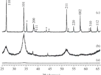
Figure 2 shows typical XRD patterns for all the samples. With
the exception of peaks from the Al2O3 substrate, all the peaks can
be indexed to the tetragonal rutile structure of tin oxide (JCPDS card 41-1445). The grain sizes of the as-deposited and heat-treated sputtered samples (Figures 2a and 2b) are very small, as indicated by the broad peaks in the diffractogram. The film heat-treated in air at 500 °C for 30 minutes (Figure 2b) exhibits a higher degree of cristallinity with partial (101) preferential orientation. The peaks from the doctor bladed films (Figure 2c) show no preferential orientation, being narrow and intense (comparable with typical results for bulk samples) due to the large grains sizes.
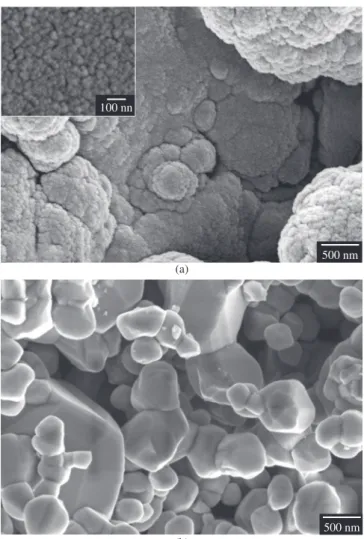
Figure 3 presents high-resolution FE-SEM images of films deposited by sputtering (Figure 3a) and doctor blade (Figure 3b), respectively. The as-deposited sputtered tin oxide thin films ( Figure 3a) show good uniformity with very small grains; the grain size is approximately 30 nm, as can be observed in the inset. The apparent aggregates present in the SEM image are actually due to the conformal tin oxide films closely following the surface topography of the unpolished alumina substrates. This is a typical result for sput-ter - coated samples. The cross section images (acquired from the sample deposited onto silicon substrates) revealed a film thickness of approximately 500 nm. After the heat treatment, the mean grain size increases to approximately 50 nm with small cracks appearing on the film surface as a consequence of the onset of sintering. For the doctor-bladed samples, one can observe in Figure 3b that the grain
4 mm
gap
Au electrodes
Alumina substrate
15 mm
SnO2 film
Figure 1. Schematic drawing showing the geometry and dimensions for the sputtered and doctor-bladed samples.
Figure 2. X ray diffraction patterns of films obtained by: a) sputtering, as deposited; b) sputtering, after heat treatment and c) doctor blade. The peaks marked with an asterisk are from the alumina substrate.
110 101
200
111
211
220
002
310 112
*
* * * *
(c)
(b)
(a)
2θ(degrees)
sizes are less uniform and at least ten times larger than the sputtered
ones. The film presents bigger pores, being approximately 100 μm
thick after the heat treatment.
Figure 4 shows the electrical resistance of the sensors with time, after changing the surrounding atmosphere from nitrogen to oxygen
and back to nitrogen. The measurements were conducted at 150 and 200 °C for both doctor bladed and sputtered samples. The electrical resistance increases with the injection of oxygen, as expected for an n-type semiconductor. At 150 °C working temperature, the resist-ance of the doctor bladed films increases by more than one order of magnitude, whereas for the sputtered sample the effect is smaller. The response of the sensors is relatively fast, with the resistance stabilizing after approximately 10 minutes for doctor bladed and 15 minutes for sputtered samples. The best response, both in terms of sensibility and response time, was obtained for the doctor bladed film, which also exhibits the steadiest behavior at 200 °C. When the atmosphere is changed back to nitrogen, the resistance drops and the final values registered are similar to the initial values.
The improved performance of the doctor bladed samples when compared to the sputtered ones can be explained by their lower initial resistance values (better sensitivity), bigger grain sizes and higher
500 nm 100 nn
500 nm (a)
(b)
Figure 3. FE-SEM images of the films deposited by: a) sputtering and b) doctor-blade techniques. The inset shows a higher magnification where the small sputtered grains can be observed.
1 x 10⁶
1 x 10⁷
1 x 10⁵
1 x 10⁵
0 0
2 x 10⁵
2 x 10⁶ 2 x 10⁶
4 x 10⁶ 4 x 10⁶
6 x 10⁶ 6 x 10⁶
2 x 10⁵
3 x 10⁵
3 x 10⁵
5 x 10⁵
1 x 10⁵
Z’ ( )
Z” (
)
0 0
5 x 10⁴ 1 x 10⁵
5 x 10³ Doctor blade
Sputtering
Heat-treated sputtering
(a)
0 0
1 x 10⁴ 1 x 10⁴ 1 x 10⁷
1 x 10⁷ 1 x 10 6
1 x 10⁶
1 x 10³
1 x 10³
1 x 10⁶
1 x 10⁷
1.85 x 10⁷
2 x 10³ 3 x 10³
0 0
2 x 10⁴ 2 x 10⁴
2 x 10³
3 x 10⁴ 3 x 10⁴
3 x 10³
4 x 10⁴ 4 x 10⁴
5 x 10⁴ 5 x 10⁴
Z’ ( )
Z” (
)
1.85 x 10⁷
(b)
0 500 1000 1500 2000 2500 3000 3500 4000
Time (seconds)
Resistance (
)
Sputtering 150 °C Doctor blade 150 °C Sputtering 200 °C Doctor blade 200 °C
Figure 4. Changes in the electrical resistance with time for doctor-bladed and sputtered samples kept in nitrogen, exposed to oxygen and back to nitrogen atmosphere at 150 and 200 °C.
porosity (faster response times). The sensitivity and the response times are better for all samples at the 200 °C working temperature (Figure 4) due to the higher rate of gas adsorption/desorption at elevated temperatures.
Resistance vs. time curves can be understood considering the existence of potential barriers between grains that are responsible for the change in the electrical response of the material. The interaction of oxygen with grain surfaces produces the transfer of electrons from the bulk to the surface. From this process, the barrier height and the depletion width become larger and, as a consequence, the sample
resistance increases21. The impedance of polycrystalline samples is
described by a complex behavior, due to the contribution of different system components like grain boundaries, grains, pores and metal-lic contacts. The impedance responses in air, for the 50 and 350 °C temperatures selected for data analysis are presented in Figure 5. The
disordered deep bulk trap location in SnO2 grains could be the
phe-nomenon that modifies the Debye-like response. Usually the electrical behavior of tin oxide thick films is modeled with an (RC) parallel
equivalent circuit. However, in our previous works23,24 regarding the
impedance frequency response technique, experiments have shown that a more sophisticated model should be considered. Distinctively, expected deep traps, with a distribution of activation energies, imply a distributed impedance element (Davidson-Cole model). The electrode effects could also be incorporated, but primarily a single semicircle could be usually attributed to a single relaxation process, indicating that at the measured-frequency range and at 50 °C (Figure 5a) only the semicircle corresponding to the grain boundary contribution is observed8.
As one can notice for the 350 °C working temperature ( Figure 5b), in the high frequency region the semicircles exhibit a small deforma-tion, indicating the presence of a second time constant due to the con-tribution from the grains. The electrical resistance at low frequencies, measured at 350 °C, is at least two orders of magnitude smaller than the one measured at 50 °C. This can be assigned to the temperature influence on the conductivity of n-type semiconductors, which also improves the oxygen diffusion across the film.
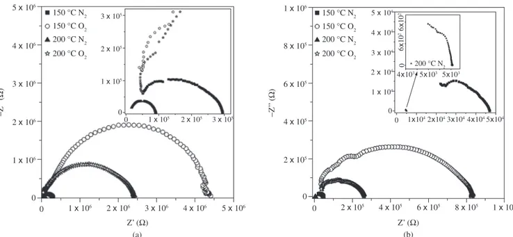
Further measurements were performed in order to study the response of devices with dissimilar grain sizes upon exposure to
different gases. Figure 6 show the Nyquist plots of the sputtered and doctor bladed films measured in oxygen and nitrogen at 150 and 200 °C. As can be noticed, the surrounding atmosphere has a large influence in the electrical behavior of the sensors. The impedance plots for both nanocrystalline (Figure 6a) and microcrystalline (Figure 6b) samples are formed by two arcs showing, once again, the existence of a second time constant. The formation of the second semicircle at high frequencies points out the contribution of the bulk grains to the electrical behavior of the films. In our case, the influence of electrodes can be neglected in the impedance measurements.
The increasing concern in the detection of toxic and flammable gases calls for the development of highly sensitive devices. The
inter-est has long been more focused in the variation of Rgb measured at low
Zreal frequencies than in the deep trap contributions. The pattern of
the Nyquist diagrams at low frequencies reveals the changes that take place in the grain boundary region of the sensors. The deformation of the plot is more evident for the doctor bladed film at the lowest temperature of 150 °C used for impedance analyses in gas atmosphere. This behavior is due to the chemical reaction at the surface and in the grain boundary region that takes place when oxidizing agents are present in the surrounding atmosphere. The presence of nitrogen helps removing the oxygen adsorbed at the surface of the grains, reducing the sample resistivity. Oxidizing agents lead to a depletion of charge carriers within the surface layer and grain boundaries, whereas reduc-ing agents, due to desorption of oxygen, increase the charge carrier
concentration4. This chemical reaction also changes the disordered
deep bulk trap location in SnO2 grains and this phenomenon could
be also modifying the Debye-like response.
4. Conclusions
The influence of the deposition techniques over the microstruc-ture and electrical properties of tin oxide thin and thick films were studied in this work. X ray diffraction patterns revealed that, for the two depositions methods, the films are composed of rutile tin oxide. FE-SEM images showed that the sputtered samples had uniform equiaxial grains having a mean particle size of approximately 30 nm, whereas the doctor bladed films exhibited less uniform grains, at least
5 x 10⁶
5 x 10⁶ 4 x 10⁶
4 x 10⁶ 3 x 10⁶
3 x 10⁵
3 x 10⁵
3 x 10⁶ 2 x 10⁶
2 x 10⁵
2 x 10⁵
2 x 10⁶ 1 x 10⁶
1 x 10⁵
1 x 10⁵
1 x 10⁶ 0
0
Z’ ( )
Z’
’ (
)
150 °C N2
150 °C O2
200 °C N2
200 °C O2
(a)
150 °C N2
150 °C O2 200 °C N2
200 °C O2
Z’ ( )
Z’
’ (
)
1 x 10⁶
1 x 10⁶ 8 x 10⁵
8 x 10⁵ 6 x 10⁵
6 x 10⁵ 4 x 10⁵
4 x 10⁵ 2 x 10⁵
2 x 10⁵ 0
0
5 x 10⁴
4 x 10⁴
3 x 10⁴
2 x 10⁴
1 x 10⁴
1x1042x1043x1044x1045x104
0 0
200 °C N2
6
x
10
2
6
x
10
2
0
4x10³ 5x10³ 5x10³
(b)
ten times larger than the sputtered ones. Atmospheres have a strong influence over the grains and grain boundaries, dictating the electri-cal behavior of the devices. The electrielectri-cal resistance of the samples made by both methods was strongly influenced by the atmosphere,
even at the relatively low working temperature of 150 °C. The good
sensing performance of the doctor bladed samples can be explained by their lower initial resistance values, bigger grain sizes and higher porosity. The improved sensitivity and response times at the 200 °C working temperature are due to the higher rate of gas adsorption/ desorption. The impedance plots as a function of temperature and gas indicated the existence of two time constants related to the grains and the grain boundaries. The contribution of the grains to the electrical behavior of the films led to the formation of a second semicircle at high frequencies and the pattern of the Nyquist diagrams at low frequencies revealed the changes that took place in the grain boundary region. Work is now in progress for the construction of a theoretical model that could help in understanding and quantifying these contributions.
Acknowledgements
The authors gratefully acknowledge the financial support from the Brazilian research funding agencies FAPESP and CNPq.
References
1. Eranna G, Joshi BC, Runthala DP, Gupta RP. Oxide Materials for Development of Integrated Gas Sensors-A Comprehensive Review. Critical Reviews in Solid State and Materials Sciences. 2004; 29(3-4):111-188.
2. Chakraborty S, Sen A, Maiti HS. Complex plane impedance plot as a figure of merit for tin dioxide-based methane sensors. Sensors and Actuators B-Chemical. 2006; 119(2):431-434.
3. Hetznecker A, Kohler H, Guth U. Enhanced studies on the mechanism of gas selectivity and electronic interactions of SnO2/Na+-ionic conductors. Sensors and Actuators B-Chemical. 2007; 120(2):378-385.
4. Hulser TP, Wiggers H, Kruis FE, Lorke A. Nanostructured gas sensors and electrical characterization of deposited SnO2 nanoparticles in ambient gas atmosphere. Sensors and Actuators B-Chemical. 2005; 109(1):13-18.
5. Hwang JH, Edwards DD, Kammler DR, Mason TO. Point defects and electrical properties of Sn-doped In-based transparent conducting oxides. Solid State Ionics. 2000; 129(1-4):135-144.
6. Heilig A, Bârsan N, Weimar U, Schweizer-Berberich M, Gardner JW, Göpel W. Gas identification by modulating temperatures of SnO2-based thick film sensors. Sensors and Actuators B-Chemical. 1997; 43(1-3): 45-51.
7. Sakai G, Baik NS, Miura N, Yamazoe N. Gas sensing properties of tin oxide thin films fabricated from hydrothermally treated nanoparticles: Dependence of CO and H2 response on film thickness. Sensors and Actuators B-Chemical. 2001; 77(1-2):116-121.
8. Ling Z, Leach C, Freer R. A time resolved study of the response of a WO3 gas sensor to NO2 using AC impedance spectroscopy. Sensors and Actuators B-Chemical. 2002; 87(2):215-221.
9. Ghiotti G, Chiorino A, Martinelli G, Carotta MC. Moisture effects on pure and Pd-doped SnO2 thick films analysed by FTIR spectroscopy and conductance measurements. Sensors and Actuators B-Chemical. 1995; 25(1-3):520-524.
10. Vlachos DS, Papadopoulos CA, Avaritsiotis JN. Dependence of sensitivity of SnOx thin-film gas sensors on vacancy defects. Journal of Applied Physics. 1996; 80(10):6050-6054.
11. Zakrzewska K, Radecka M, Przewoznik J, Kowalski K, Czuba P. Microstructure and photoelectrochemical characterization of the TiO2– SnO2 system. Thin Solid Films. 2005; 490(1): 101-107.
12. Serrini P, Briois V, Horrillo MC, Traversa A, Manes L. Chemical composition and crystalline structure of SnO2 thin films used as gas sensor. Thin Solid Films. 1997; 304(1-2):113-122.
13. Gutierrez J, Getino J, Horrillo MC, Ares L, Robla JI, Garcıa C, Sayago I. Electrical characterization of a thin film tin oxide sensor array for VOCs detection. Thin Solid Films. 1998; 317(1-2):429-431.
14. Ryzhikov AS, Shatokhin AN, Putilin FN, Rumyantseva MN, Gaskov AM, Labeau M. Hydrogen sensitivity of SnO2 thin films doped with Pt by laser ablation. Sensors and Actuators B-Chemical. 2005; 107(1):387-391.
15. Choi YH, Hong SH. H2 sensing properties in highly oriented SnO2 thin films. Sensors and Actuators B-Chemical. 2007; 125(2):504-509.
16. Bârsan N, Weimar U. Understanding the fundamental principles of metal oxide based gas sensors; the example of CO sensing with SnO2 sensors in the presence of humidity. Journal of Physics: Condensed Matter. 2003; 15(20):R813-R839.
17. Bârsan N, Koziej D, Weimar U. Metal oxide-based gas sensor research: How to?. Sensors and Actuators B-Chemical. 2007; 121(1):18-35.
18. Liewhiran C, Phanichphant S. Effects of palladium loading on the response of a thick film flame-made ZnO gas sensor for detection of ethanol vapor. Sensors. 2007; 7(7):1159-1184.
19. Liewhiran C, Phanichphant S. Influence of thickness on ethanol sensing characteristics of doctor-bladed thick film from flame-made ZnO nanoparticles. Sensors. 2007; 7(2):185-201.
20. Liewhiran C, Phanichphant S. Improvement of flame-made ZnO nanoparticulate thick film morphology for ethanol sensing. Sensors. 2007; 7(5):650-675.
21. Ponce MA, Aldao CM, Castro MS. Influence of particle size on the conductance of SnO2 thick films. Journal of the European Ceramic Society. 2003; 23(12):2105-2111.
22. Montenegro A, Ponce MA, Castro MS, Rodríguez-Paez JE. J. SnO2-Bi2O3 and SnO2-Sb2O3 gas sensors obtained by soft chemical method. Journal of the European Ceramic Society. 2007; 27(13-15): 4143-4146. 23. Ponce MA, Bueno PR, Varela J, Castro MS, Aldao CM. Impedance
spectroscopy analysis of SnO2 thick-films gas sensors. Journal of Materials Science: Materials in Electronics. 2008; 19(12): 1169-1175.