Repositório ISCTE-IUL
Deposited in Repositório ISCTE-IUL:
2020-07-24
Deposited version:
Post-print
Peer-review status of attached file:
Peer-reviewed
Citation for published item:
Naseri, P., Costa, J. R., Matos, S., Fernandes, C. A. & Hum, S. V. (2020). Equivalent circuit modeling
to design a dual-band dual linear-to-circular polarizer surface. IEEE Transactions on Antennas and
Propagation. 68 (7), 5730-5735
Further information on publisher's website:
10.1109/TAP.2020.2963949
Publisher's copyright statement:
This is the peer reviewed version of the following article: Naseri, P., Costa, J. R., Matos, S.,
Fernandes, C. A. & Hum, S. V. (2020). Equivalent circuit modeling to design a dual-band dual
linear-to-circular polarizer surface. IEEE Transactions on Antennas and Propagation. 68 (7), 5730-5735,
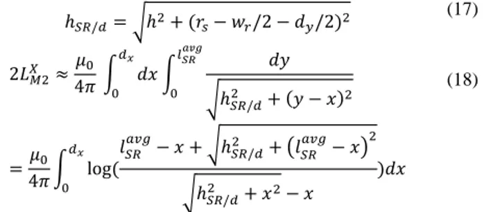
which has been published in final form at https://dx.doi.org/10.1109/TAP.2020.2963949. This article
may be used for non-commercial purposes in accordance with the Publisher's Terms and Conditions
for self-archiving.
Use policy
Creative Commons CC BY 4.0
The full-text may be used and/or reproduced, and given to third parties in any format or medium, without prior permission or charge, for personal research or study, educational, or not-for-profit purposes provided that:
• a full bibliographic reference is made to the original source • a link is made to the metadata record in the Repository • the full-text is not changed in any way
The full-text must not be sold in any format or medium without the formal permission of the copyright holders.
Serviços de Informação e Documentação, Instituto Universitário de Lisboa (ISCTE-IUL) Av. das Forças Armadas, Edifício II, 1649-026 Lisboa Portugal
Phone: +(351) 217 903 024 | e-mail: [email protected] https://repositorio.iscte-iul.pt
Abstract—The working principle of a thin dual-band dual-linear to circular polarizer is presented here. This polarizer not only converts incident linearly polarized (LP) waves to circularly polarized (CP) waves in two frequency bands, but it also reverses the handedness of each signal. The electromagnetic behavior of the cell is carefully analyzed and two equivalent circuit models (ECMs) are presented to model the responses of the cell to linearly-polarized waves at normal incidence. The ECMs show how utilizing interlayer coupling can be leveraged to achieve reversed CP senses in two bands using a compact design. Analytical formulas are presented to provide initial values of the ECM components including the mutual coupling inductances. We present measurement results that agree well with the full-wave simulation and the ECM results, thus validating the proposed ECM model.
Index Terms—Polarizers, frequency selective surfaces, circular
polarization, equivalent circuits, dual-band. I. INTRODUCTION
For many applications such as point-to-point and satellite communications, there is an increasing demand to employ circularly polarized (CP) antennas at the transmitting and receiving ends [1]. Integration of a linearly polarized (LP) antenna with a suitable planar linear-to-circular polarization converter [2]-[6] (simply called a polarizer here) can simplify the design and fabrication of CP antennas. For example, for dual K/Ka-band satellite communications, it is not only required that there be separate transmitting (TX) and receiving (RX) bands, but that the radiated CP waves in these bands must also have opposite senses. Moreover, for handover purposes in multi-spot coverage schemes, it is important that the polarizer operates for both linear polarizations and converts them to both to CP in each band. Implementing the latter at the radiating aperture level is quite challenging considering that it still needs to provide dual-band operation as well. Therefore, for this application, a unique polarizer [7] that can convert LP to CP in two frequency bands with opposite senses can potentially reduce the required number of apertures used to implement multi-beam coverage patterns.
The full analysis of the polarizer cell was out of the scope of our previous publication [7]. There, we explained the role of the printed elements and the relationship between their dimensions to the resonances. The polarizer has an ultra-thin profile of only 10.5% of wavelength in the higher frequency band. During the development of this polarizer, we made an interesting observation: that the inevitable mutual coupling can be used in our favor and produce the necessary distinct resonance effects between x- and y-polarizations. This promoted further investigation of the dynamics of the polarizer, resulting in a detailed analysis presented in this Communication. Here, we show that the interlayer mutual coupling between elements is the
Manuscript received Dec. 2018. This work is partially supported by MDA and by Fundação para a Ciência e Tecnologia (FCT) under projects PTDC/EEI-TEL/30323/2017 (“ADAM3D”) and UID/EEA/50008/2019. Parinaz Naseri and Sean V. Hum are with the Edward S. Rogers Sr. Department of Electrical & Computer Engineering, 10 King’s College Road Toronto, Ontario, Canada, M5S 3G4 (e-mail: [email protected]).
key factor in the unique response of the polarizer. Lack of understanding of this coupling may lead to avoidable excessive iterative cycles of optimization without leading to the best possible response. The model we develop in this can address this issue.
We start the analysis of the polarizer from our previous design [7]. Based on the operational principle and the certain response of this polarizer to each LP incident wave, we develop two decoupled ECMs to model the polarizer. We present analytical formulas to extract most of the ECM components including the mutual inductances between layers. The ECMs are used to explain the working principle and the particular electromagnetic behavior of the cell. These ECMs can also be deployed as surrogate models for fast analysis. We validate the ECMs for a new example of the polarizer.
The paper is organized as follows. In Section II, the working principle of the dual-band polarizer unit cell [7] is explained and two new ECMs are presented to represent its responses to x- and y-polarized incident fields. In Section III, the analytical formulas to obtain initial estimations of the ECM components are presented. An example of the unit cell is designed and the ECMs are validated by comparison with the full-wave simulation results in Section IV. Conclusions are drawn in Section V.
II. WORKING PRINCIPLE OF THE PROPOSED DUAL-BAND POLARIZER
UNIT CELL
The proposed unit cell is composed of three metallic layers stacked with two thin low-permittivity substrates [7], as shown in Fig. 1. The first and the third layers are identical and composed of split rings and patch elements. The middle layer is composed of a circular slot and a dipole. The whole thickness of the unit cell is 1.05 mm, which is 7% and 10.5% of the wavelength at the lower and higher center frequencies, respectively.
To obtain the unique property of this polarizer, i.e. converting LP to CP in two frequency bands with opposite senses, it is required to generate +90 and -90 phase differences between the transmitted x and y waves in the lower and higher frequency bands, respectively, or vice versa for switching the polarization. Such a feature is achieved using resonant asymmetric elements along x- and y-axes to obtain anisotropic response in the unit cell.
To obtain an understanding of the working principle of the unit cell, we model it by employing ECMs for waves at normal incidence polarized along x- and y-axes. As the first step, we assume that the different layers of the unit cell are initially decoupled, but as we develop the model, different interlayer coupling mechanisms are modeled by augmenting the ECM. Therefore, with no interlayer coupling in the unit cell and no mutual coupling between the unit cell and its adjacent neighbors, the three-layer structure of the unit cell can be simply modeled by cascading the ECMs of each layer [8]. Since the
Jorge R. Costa, Sérgio A. Matos and Carlos A. Fernandes are with Instituto de Telecomunicações, Instituto Superior Técnico, Universidade de Lisboa, Av. Rovisco Pais 1, 1049-001 Lisboa, Portugal. Jorge R. Costa and Sérgio A. Matos are also with Instituto Universitário de Lisboa (ISCTE-IUL), Departamento de Ciências e Tecnologias da Informação Av. das Forças Armadas, 1649-026 Lisboa, Portugal.
Equivalent Circuit Modeling to Design a Dual-Band Dual
Linear-to-Circular Polarizer Surface
Parinaz Naseri, Student Member, IEEE, Jorge R. Costa, Senior Member, IEEE, Sérgio A. Matos,
Member, IEEE, Carlos A. Fernandes, Senior Member, IEEE, Sean V. Hum, Senior Member, IEEE
unit cell is intentionally not composed of any significantly lossy material, lossless ECMs are developed here.
Fig. 1. (a) The identical first and the third layers, (b) the second layer, and (c) the 3D view of the unit cell.
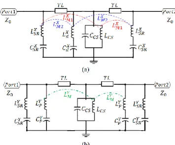
The complete ECMs of the unit cell for both polarization are shown in Fig. 2, where the patch and the split rings on the first and the third layers, and the dipole in the middle layer can each be modeled by a set of series LC resonators. The equivalent components associated with these are shown as (𝐶𝑝, 𝐿𝑝) for the patch, (𝐶𝑆𝑅, 𝐿𝑆𝑅) for the split ring,
and (𝐶𝑑, 𝐿𝑑) for the dipole. Due to complementary shape of the circular
slot to a circular patch, it is modeled by the dual of the series capacitance and inductance, which is a shunt LC resonator (𝐶𝐶𝑆, 𝐿𝐶𝑆).
Since the incident electric field couples to the elements of each layer simultaneously, each constituent resonator is in parallel with the others in the same layer [9]. The thin substrates between the metallic layers of the unit cell are each modeled as transmission lines with a thickness of ℎ and a characteristic impedance of 𝑍 = 𝑍0⁄√𝜀𝑟, where 𝑍0≈
377 𝛺 is the free-space characteristic impedance and 𝜀𝑟 is the
permittivity of the substrate.
The asymmetric metallic parts of the unit cell along x- and y-axes requires that two circuit models be used to mimic the response of the unit cell to an x- and y-polarized incident waves. It can be shown that the cross-polarization coefficients such as |S11xy| = |S11yx| = |S21xy| = |S21yx| ≈ 0 [10].Therefore, we can assume there is negligible coupling between the responses of the unit cell to the two electric field polarizations and model each response with a specific ECM independent from the other. We separate the analysis of the unit cell for an x- and y-polarized incident fields in the following descriptions. Based on the components of the unit cell shown in Fig. 1, the patches on the first and the third layers mainly impact the response of the unit cell to a y-polarized incident field and are modeled by (𝐶𝑃𝑌, 𝐿𝑃𝑌). The dipole on the second layer mainly impacts the
response of the unit cell to an x-polarized incident field and is modeled by (𝐶𝑑𝑋, 𝐿
𝑑
𝑋). Moreover, the split rings have distinct responses to x- and
y-polarized incident fields, resulting in two sets (𝐶𝑆𝑅𝑋, 𝐿𝑆𝑅𝑋 ) and
(𝐶𝑆𝑅𝑌, 𝐿𝑆𝑅𝑌 ), respectively. The circular slot is symmetric and can be
modeled by (𝐿𝐶𝑆, 𝐶𝐶𝑆) for both x- and y-polarized incident waves.
The split rings and their responses to the x-polarized and y-polarized incident fields need more clarification. Their different behavior to the two orthogonal LP fields and their tight coupling plays a key role in achieving opposite handedness of the transmitted CP waves in the two bands. Therefore, it is important to closely look at the differences when the split rings are excited by the x- and y-polarized fields.
Fig. 2. The complete ECMs of the unit cell to (a) x-polarized and (b) y-polarized fields at normal incidence.
Fig. 3 (a) and (d) present the magnitude of the excited surface currents in the complete ring when it is excited by an x- and y-polarized incident wave, respectively, at the resonant frequency of the complete ring without the gaps. Fig. 3 (b) and (c) shows the direction and magnitude of the excited surface currents when the incident wave is x-polarized at 23 GHz. Fig. 3 (e) and (f) show the surface currents when it is excited by a y-polarized wave at the same frequency. The dimensions of the complete ring and the split ring are provided in Table I. The unit cell simulations were conducted using periodic boundary conditions in Ansys HFSS [11].
By comparing Fig. 3 (a) with Fig. 3 (b) and (c), it can be concluded that introducing the gaps in the ring does not have major effect on the response of the unit cell to an x-polarized incident wave. However, by comparing Fig. 3 (d) with Fig. 3 (e) and (f), it can be easily seen that the introduced gaps cause significant interruption in the induced currents of the ring when it is excited by a y-polarized field. Therefore, for a y-polarized incident wave, the gaps significantly reduce the effective length of the ring. As a result, one should expect 𝐿𝑆𝑅𝑌 to have
smaller value compared to its counterpart 𝐿𝑆𝑅𝑋 . Therefore, the split ring
resonates at a much higher frequency when it is excited with y-polarized field compared to its resonance to an x-y-polarized field.
The net effect of this is that the transmission coefficient of the unit cell to a y-polarized field, 𝑆21𝑦𝑦, has no null in the band. Nevertheless, the split ring resonates for an x-polarized field in the band of interest and the transmission coefficient, 𝑆21𝑥𝑥, has one null in the band. This
creates a situation where arg(𝑆21𝑥𝑥) − arg(𝑆21𝑦𝑦) < 0 in the low band
and arg(𝑆21𝑥𝑥) − arg(𝑆21 𝑦𝑦
) > 0 in the high band. Moreover, by using thin substrates and ensuring sufficient mutual coupling between the layers, the structure’s 𝑆21𝑥𝑥 can have two nulls, while 𝑆21
𝑦𝑦
has no null in the band. This causes the phase of 𝑆21𝑥𝑥 to have two 180° jumps, a
360° jump in total, along the band. Therefore, it is possible to have −90° phase difference and +90° respectively in the lower band and the higher band.
For an x-polarized field, the split rings strongly resonate and generate a magnetic flux passing the second layer. Therefore, for x-polarized field, it can be concluded that there is strong magnetic coupling between the split rings of the first and the third layers and the inductances of the dipole and circular slot on the second layer. These couplings are modelled by mutual inductances, i.e. 𝐿𝑀1𝑋 and 𝐿𝑀2𝑋
between each split ring and the circular slot and each split ring and the dipole respectively. It is worth noting that the interlayer coupling is mostly inductive and capacitive coupling is negligible [12].
For a y-polarized field, by introducing the gap, we make the split ring non-resonant in the bands of interest. Therefore, the split rings
show very weak and negligible magnetic and capacitive coupling to the other elements for a y-polarized incident wave. However, the patches on the first and the third layers are resonant for a y-polarized field. The excited currents on them generate a magnetic flux that couples to the elements of the second layer. Therefore, there is magnetic coupling between the inductance of each patch and the inductance of the circular slot. This magnetic coupling is modeled by 𝐿𝑀𝑦 in Fig. 2 (b).
Fig. 3. The magnitude of the surface current of a complete ring and split ring to normal incidence x-polarized: (a)-(c) and y-polarized (b)-(d) incident waves at the resonance frequency of the complete ring. All figures have the same scale.
III. ANALYTICAL FORMULATION OF THE ECMCOMPONENTS
An initial estimation for the component values in Fig. 2 can be obtained using the following equations:
Based on 𝑤 and 𝑟𝑠, an initial value for 𝐿𝐶𝑆 can be calculated using
(1)-(2) based on duality theory and using (1) in [13] and (2) in [14], where 𝑔 = 𝑤 − 2𝑟𝑠. Moreover, 𝐶𝐶𝑆 can be estimated using (3),
where 𝜀𝑒𝑓𝑓𝑑= (𝜀𝑟+ 𝜀𝑟)/2 = 𝜀𝑟 since the circular slot is between
two dielectric layers [15]. 𝑔̅𝑓𝑢𝑙𝑙= 1 8(𝑔2− 𝑤)[2(1 + √2)𝑔 2+ (𝜋 − 4)𝑤2 − ((2 + √2)𝜋 − 4) 𝑔𝑤] (1) 𝐿𝐶𝑆≈ 𝜇0 𝑤 2𝜋ln ( 1 sin(𝜋𝑔̅2𝑤𝑓𝑢𝑙𝑙) ) (2) 𝐶𝐶𝑆= 𝜀0√ 𝜀𝑒𝑓𝑓𝑑 2𝑤 𝜋 ln ( 1 sin(𝜋𝑔̅2𝑤𝑓𝑢𝑙𝑙) ) (3)
Based on the dimensions of the dipole, i.e. 𝑑𝑥 and 𝑑𝑦, the inductance
of the dipole can be explained by approximating the dipole and its adjacent neighbor as two parallel finite wires [9]. Therefore, 𝐿𝑑𝑋 and
𝐶𝑑𝑋can be calculated based on (4)-(5) [16]:
𝐿𝑑𝑋≈ 𝜇0 2𝜋𝑤 ln ( 1 sin(𝜋(𝑤 − 𝑑2𝑤 𝑥)) ) (4) 𝐶𝑑𝑋≈ 𝜀0√ 𝜀𝑒𝑓𝑓𝑑 4𝑟𝑠 𝜋 ln ( 1 sin(𝜋(2𝑟𝑠− 𝑑𝑥) 4𝑟𝑠 ) ) (5)
Please note that in the calculation of 𝐶𝑑𝑋, 2𝑟
𝑠 is considered to be the
period of the cell instead of 𝑤. By this adjustment, we approximately capture the capacitance of the dipole and the mutual capacitance between the dipole and the circular slot by 𝐶𝑑𝑋 without introducing
complexity to the ECM.
Based on the size of the patch components on the first and the third layers, i.e. 𝑃𝑦, its 𝐶𝑃𝑌 capacitance [14] and 𝐿𝑃𝑌 inductance [16] for a
y-polarized incident wave can be calculated based on (6)-(7), where 𝜀𝑒𝑓𝑓= (𝜀𝑟+ 1)/2 [15]: 𝐶𝑃𝑌≈ 𝜀0√ 𝜀𝑒𝑓𝑓 2𝑤 𝜋 ln ( 1 sin(𝜋(𝑤 − 𝑃2𝑤 𝑦)) ) (6) 𝐿𝑌𝑃≈ 𝜇0 2𝜋𝑤 ln ( 1 sin(𝜋(𝑤 − 𝑃2𝑤 𝑦)) ) (7) Based on 𝑟𝑠 and 𝑤𝑟, and G, the self-inductance of the split ring for
x-polarization, i.e. 𝐿𝑆𝑅𝑋 , can be calculated as the sum (8) of a proportion
(9) from the complete ring [17], i.e. 𝐾𝐿𝐶𝑅/4, and the mutual
inductance between the two halves of the split ring (11), i.e. 𝐿𝑀𝑆𝑅.
𝐾𝐿𝐶𝑅/4 is calculated with uniform amplitude of surface current
across the ring, see Fig. 4 (a), where 𝑟𝑖= 𝑟𝑠− 𝑤𝑟. 𝐾 captures the
length reduction of the split ring due to the gap. 𝐿𝑆𝑅𝑀 can be calculated
using Neumann’s formula (11) [18]. The capacitance of the split ring can be calculated based on the resonance of the split ring, i.e. 𝑓0, in
(13), and its inductance. 𝐿𝑆𝑅𝑋 = ( 𝐾𝐿𝐶𝑅 2 + 𝐿𝑆𝑅 𝑀)/2 (8) 𝐾𝐿𝐶𝑅 4 ≈ 𝐾 4 𝜇0𝜋3 4𝑤𝑟2 ∫ 1 𝑘2 ∞ 0 [𝑟𝑠ẞ(𝑘𝑟𝑠) − 𝑟𝑖ẞ(𝑘𝑟𝑖)]2𝑑𝑘 (9) ẞ(𝑥) = 𝑆0(𝑥)𝐽1(𝑥) − 𝑆1(𝑥)𝐽0(𝑥) (10) 𝐿𝑆𝑅𝑀 = 𝜇0𝑟𝑠 4𝜋 ∫ ∫ cos (𝜑1+ 𝜑2)𝑑𝜑1𝑑𝜑2 √2(1 − cos (𝜑1+ 𝜑2)) 𝜋−𝜑0 𝜑0 𝜋−𝜑0 𝜑0 (11) 𝜑0= sin−1 ( 𝐺 2𝑟𝑠− 𝑤𝑟); 𝐾 = 1 − 2𝜑0 𝜋 (12) 𝐶𝑆𝑅𝑋 = 1 (2𝜋𝑓0)2𝐿𝑆𝑅𝑋 ; 𝑓0= 𝑐 (2𝜋𝑟𝑠− 2𝐺)√ 𝜀𝑒𝑓𝑓 (13)
In these equations, 𝑆𝑛 and 𝐽𝑛 are the nth order Struve and Bessel
functions, respectively [17].
As mentioned earlier, the gaps significantly disturb the response of the ring to a y-polarized wave. Fig. 4 (b) shows the total inductance of the split ring to a y-polarized wave. It shows the self-inductance of the split ring for y-polarization, i.e. 𝐿𝑆𝑅𝑌 , is almost 𝐾𝐿𝐶𝑅/16. The
mutual inductance between the parts of the split ring can be calculated to be negligible. The capacitance of the split ring for both polarizations is approximately equal.
𝐿𝑆𝑅𝑌 ≈ 𝐾𝐿𝐶𝑅/16 , 𝐶𝑆𝑅𝑌 ≈ 𝐶𝑆𝑅𝑋 (14)
Fig. 4. The equivalent components of the split ring for (a) x-polarized and (b) y-polarized waves at normal incidence, where 𝐶𝐶𝑅 and 𝐿𝐶𝑅 are
surface current vectors are shown at the resonance frequency of the complete ring.
The mutual inductance between each half of the split ring and the circular slot when excited with x-polarized wave, i.e. 2𝐿𝑀1𝑋 , can be
crudely approximated as that between two wires of the same length [18]. Based on the current distribution that is similar to the one excited on the circular slot [see Fig. 5 (a)], the mean effective length of half split ring, i.e. 𝑙𝑆𝑅𝑎𝑣𝑔, and 2𝐿𝑀1𝑋 can be calculated using
(15) and Neumann’s formula (16). We note that the term in the brackets of (15) is the length of the arc of the half split ring and the factor 0.7172 = ∫𝜋−𝜑0𝐼(𝜑)𝑑𝜑
𝜑0 / (𝑚𝑎𝑥 (𝐼(𝜑))(𝜋 − 2𝜑0)) is due to
the non-uniform amplitude of the current distribution, i.e. 𝐼(𝜑) ≈ sin (𝜑) on the split ring and 𝜑0 is calculated using (12). Moreover,
the total mutual inductance between the split ring and the circular slot is the parallel combination of two 2𝐿𝑋𝑀1, i.e., 𝐿𝑀1𝑋 .
𝑙𝑆𝑅𝑎𝑣𝑔≈ 0.7172[𝜋(𝑟𝑠− 𝑤𝑟 2) − 𝐺] (15) 2𝐿𝑋𝑀1≈ 𝜇0 2𝜋 𝑙𝑆𝑅 𝑎𝑣𝑔 [log (2𝑙𝑆𝑅 𝑎𝑣𝑔 ℎ ) − 1 + ℎ 𝑙𝑆𝑅𝑎𝑣𝑔] (16) In the same manner, the mutual inductance between each half of the split ring and each long edge of dipole, i.e. 2𝐿𝑋𝑀2, can be calculated.
The average distance between each long side of the dipole and each half split ring is ℎ𝑆𝑅/𝑑, considering the concentration of the currents
are in the middle of the split ring and the long edges of the dipole, (see Fig. 5 (b)): ℎ𝑆𝑅/𝑑= √ℎ2+ (𝑟𝑠− 𝑤𝑟/2 − 𝑑𝑦/2)2 (17) 2𝐿𝑀2𝑋 ≈ 𝜇0 4𝜋 ∫ 𝑑𝑥 ∫ 𝑑𝑦 √ℎ𝑆𝑅/𝑑2 + (𝑦 − 𝑥)2 𝑙𝑆𝑅𝑎𝑣𝑔 0 𝑑𝑥 0 =𝜇0 4𝜋∫ log ( 𝑙𝑆𝑅𝑎𝑣𝑔− 𝑥 + √ℎ𝑆𝑅/𝑑2 + (𝑙 𝑆𝑅 𝑎𝑣𝑔 − 𝑥)2 √ℎ𝑆𝑅/𝑑2 + 𝑥2− 𝑥 )𝑑𝑥 𝑑𝑥 0 (18)
To find an initial estimation of the mutual inductance between the patches and the circular slot, i.e. 2𝐿𝑌𝑀, the surface currents on the
patch and the circular slot are shown in Fig. 5 (c). The average distance between each long edge of the patch and half of the circular slot is ℎ𝐶𝑆/𝑃 and 2𝐿𝑀𝑌 can be calculated based on (19) by replacing
ℎ𝑆𝑅/𝑑 with ℎ𝐶𝑆/𝑃 and 𝑑𝑥 with 𝑃𝑦.
ℎ𝐶𝑆/𝑃= √ℎ2+ (𝑟𝑠− 𝑃𝑥/2)2 (19)
Fig. 5. The surface currents at 23 GHz on (a) split ring and circular slot, (b) split ring and the dipole when excited with x-polarized incident wave, and (c) the patch and the circular slot when excited with a y-polarized incident wave.
IV. ADESIGN EXAMPLE AND VALIDATION
To validate the proposed ECMs, we start from a unit cell designed to operate in a low band defined as 18.2-18.8 GHz and high band defined as 27.0-27.8 GHz. Table I summarizes the dimensions of the polarizer unit cell designed in a full-wave simulation tool, see Fig. 1. The unit cell is simulated using periodic boundary conditions in the 𝑥- and y-directions.
TABLE I
DIMENSIONS OF NEW UNIT CELL
Dimension Value (mm) Dimension Value (mm)
𝑑𝑥 2.7 𝑟𝑠 2.3
𝑑𝑦 0.45 𝐺 1.4
ℎ 0.508 𝑤 5.3
𝑃𝑥 1.1 𝑤𝑟 0.2
𝑃𝑦 3.3
To find the values of the ECM components, we use the formulas presented in Section III to obtain estimates for most of the components in Fig. 2. There is a frequency discrepancy between the reflection and transmission coefficients of the full-wave (FW) simulations and the ECMs with these analytical values, presented in Fig. 6. Therefore, a gradient-based optimization in the Advanced Design System (ADS) software [19] with the initial values of the second column of Table II is performed to improve the alignment with the full-wave simulation results. The fitted values are listed in the third column of Table II. Fitting the components provides better match to the full-wave simulation by presenting more accurate values than the ones obtained by the analytical formulas. While the analytical values and the fitted ones are from the same order of magnitude, it should be noted that the analytical formulas are derived in the absence of mutual coupling between the layers and the different components; therefore, they provide initial values for further optimization. Simplification of the ECMs and ignoring some of the elements for certain polarizations, i.e. the patches for x-polarization and the dipole for y-polarization, also introduce differences between the analytical values and the fitted ones.
TABLE II
COMPONENT VALUES OF FIG.2ECMS.
Element Analytical Value Fitted Value
𝐶𝐶𝑆 0.008 pF 0.005 pF 𝐶𝑑𝑋 0.023 pF 0.042 pF 𝐶𝑆𝑅𝑋 0.024 pF 0.018 pF 𝐶𝑃𝑌 0.023 pF 0.023 pF 𝐶𝑆𝑅𝑌 0.024 pF 0.009 pF 𝐿𝐶𝑆 1.136 nH 0.862 nH 𝐿𝑋𝑑 0.390 nH 0.242 nH 𝐿𝑋𝑀1 0.655 nH 0.741 nH 𝐿𝑋𝑀2 0.206 nH 0.221 nH 𝐿𝑆𝑅𝑋 2.361 nH 3.500 nH 𝐿𝑃𝑌 0.635 nH 0.784 nH 𝐿𝑆𝑅𝑌 0.540 nH 0.736 nH 𝐿𝑌𝑀 0.276 nH 0.208 nH 𝑍 255 Ω 255 Ω
Fig. 6. Comparison between the full-wave simulation results and the ECMs with the values of the second column of Table II.
(a)
(b)
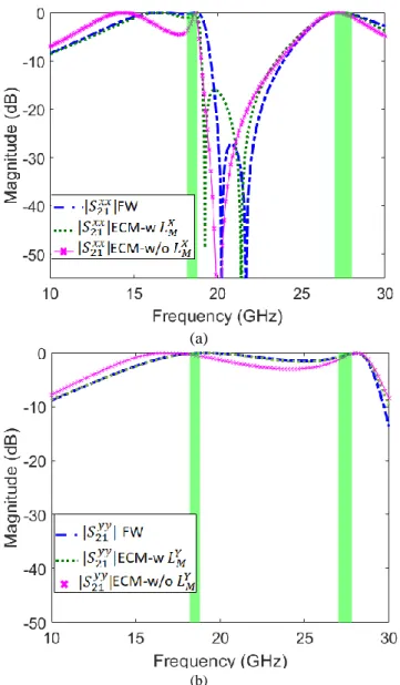
Fig. 7. Comparison between the amplitude of the scattering parameters of the presented ECMs with and without the mutual coupling in the ECMs presented in Fig. 2 (a), and the unit cell: (a) transmission coefficients, (b) reflection coefficients to an x-polarized wave at normal incidence and (c) transmission and reflections coefficients to y-polarized wave at normal incidence.
Fig. 8. Comparison between the phases of the transmission coefficients of the cell and the ECMs for x- and y-polarized waves at normal incidence.
Another important ability that the ECM provides is being able to understand the effect of inter-layer coupling on the behavior of the polarizer. For example, Fig. 7 (a)-(b) show the comparison between the amplitude of the reflection and transmission coefficients of the cell to x-polarized and y-polarized incidence fields in full-wave simulation and the responses of corresponding ECMs with the values listed in the third column of Table II simulated in ADS. In Fig. 7 (a), we compare the results of the ECM in Fig. 2 (a) with and without the mutual coupling with the full-wave simulation results. From this figure, the essential role of the mutual inductances can be easily understood. One can note that thereis a difference between the number of the nulls in |𝑆21𝑥𝑥| of the unit cell in the full-wave simulation and the corresponding
ECM without the mutual inductances. Fig. 7 (b) shows the excellent agreement between the ECM in Fig. 2 (b) and the response of the cell to a y-polarized wave. Moreover, the results of the |𝑆21𝑦𝑦| from the ECM shown in Fig. 2 (b) with and without the mutual inductance, 𝐿𝑌𝑀, are
compared with the full-wave simulation results. The mutual inductance in Fig. 2 (b) seems to have a minor effect in the transmission bandwidth in the higher band and a frequency shift in the lower band.
The better agreement in Fig. 7 (b) compared to Fig. 7 (a) can be related to our initial assumptions in the ECMs. We had assumed that the patch is negligible for an x-polarized wave and the dipole is negligible for a y-polarized wave. While the latter can be forgiving, since dy≈ 0.15dx, the first assumption can lead to the differences in
Fig. 7 (a) since 𝑃𝑥≈ 0.33𝑃𝑦. However, this difference is a small price
to keep the ECMs and the analysis simple.
Fig. 8 presents the comparison between the phases of the transmission coefficients of the cell and the ECMs. It can be seen that the difference between the phases of the 𝑆21𝑥𝑥 and 𝑆21
𝑦𝑦
is almost the same for the cell and the ECMs especially in the bands of interest, which are indicated by the green bars.
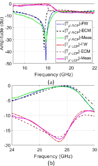
To calculate the LP to CP transmission coefficients, we excite the polarizer cell with a LP plane wave at normal incidence propagating in the z-direction, i.e. polarized in the 𝑦′-direction in Fig. 1, that has its electric field making a 45° angle to the x- and y- axes of the cell. We also measured the prototype of the polarizer detailed in Table I under normal incidence using quasi-optical setup shown in Fig. 9 in both bands. In the measurement, the fabricated polarizer unit cell is rotated by 45° and the excitations are in x- and y-directions. The results of the cell from full-wave simulation and measurements are compared to the post-processed results of the ECMs in Fig. 10. The ECM results agree
well with full-wave simulation and measurmentresults, which further validates the proposed ECMs.
Fig. 9. Quasi-optical setup with the dual-LP polarized K-band horns.
Fig. 10. Linear-to-circular transmission coefficients, i.e. |𝑇𝑦′−𝐿𝐶𝑃| and |𝑇𝑦′−𝑅𝐶𝑃|of the simulated and measured cell and the ECMs in (a) the low band,
and (b) the high band.
V. CONCLUSION
The working principle of a dual-band dual-LP to dual-CP converter can be explained using two ECMs for its responses to x- and y-polarized incident waves. Compared to previous work on this topic, we provide a thorough analysis of the electromagnetic behavior of the cell and use the proposed ECMs to show how interlayer coupling can be employed to achieve unique properties in a polarizer such as opposite handedness of the transmitted CP waves in the two bands. The development of the ECM in this paper provides a reference for readers
to develop ECMs for their structures and avoid blind parametric optimizations, in order to accelerate their design while providing additional physical insight into their operation. This unique topology of the unit cell has shown great flexibility to be changed for different applications and different frequencies [7], [20]-[21]. The information presented here can be a guideline for such changes based on the application at hand.
REFERENCES
[1] S. Gao et al., “Introduction to circularly polarized antennas,” in Circularly Polarized Antennas, Ed. UK: Wiley, 2014, pp. 1–25.
[2] L. Martinez-Lopezet et al., “A multilayer circular polarizer based on bisected split-ring frequency selective surfaces,” IEEE Antennas Wireless
Propag. Lett., vol. 13, pp. 153–156, Jan. 2014.
[3] W. Tang et al., “Low-profile compact dual-band unit cell for polarizing surfaces operating in orthogonal polarizations,” IEEE Trans. Antennas
Propag., vol. 65, no. 3, pp. 1472-1477, Mar. 2017.
[4] M. Hosseini et al., “A semianalytical approach to designing high-transparency low-profile circular polarizers,” IEEE Trans. Antennas
Propag., vol. 66, no. 12, pp. 7138-7147, Dec. 2018.
[5] S. Hassan Abadi et al., “Wideband linear-to-circular-polarization converters based on minituarized-element frequency selective surfaces,”
IEEE Trans. Antennas Propag., vol. 64, no. 2, pp. 526–534, Feb. 2016.
[6] M. Joyal et al., “Analysis and design of thin circular polarizers based on meander lines,” IEEE Trans. Antennas Propag., vol. 60, no. 6, pp. 3007-3011, Jun. 2012.
[7] P. Naseri et al., “Dual-band dual linear to circular polarization converter in transmission mode-application to K/Ka-band satellite communications,” IEEE Trans. Antennas Propag., vol. 66, no. 12, pp. 7128-7137, Dec. 2018.
[8] B. A. Munk, Frequency selective surfaces: theory and design. John Wiley & Sons, 2005.
[9] F. Costa et al., “An overview of ECM modeling techniques of frequency selective surfaces and metasurfaces,” ACES J., vol. 29, no. 12, pp. 960-976, Dec. 2014.
[10] P. Naseri et al., “Efficient evaluation of gradient transmit-arrays through an equivalent dispersive dielectric description,” IEEE Trans. Antennas
Propag., vol. 67, no. 9, pp. 5996–6007, Sep. 2019.
[11] ANSYS® High Frequency Electromagnetic Field Simulation, Release 18.0: http://www.ansys.com.
[12] G. Xu et al., “Generalized synthesis technique for high-order low-profile dual-band frequency selective surfaces,” IEEE Trans. Antennas Propag., vol. 66, no. 11, pp. 6033–6042, Nov. 2018.
[13] D. Ramaccia et al., “A new accurate model of high-impedance surfaces consisting of circular patches,” Progress in Electromag. Research
Magazine, vol. 21, pp. 1-17, 2011.
[14] M. Al-Joumayly et al., “A new technique for design of Low-profile, second order, bandpass frequency selective surfaces,” IEEE Trans.
Antennas Propag., vol. 57, no. 2, pp. 452–459, Feb. 2009.
[15] C. A. Balanis, Modern Antenna Handbook. New York, NY, USA: Wiley, 2011, pp. 779–828.
[16] M. Fallah et al., “Desgin of frequency selevtive band stop shield using analytical method,” J. Microw. Optoelectron. Electromagn. Appl., vol. 14, no. 2, pp. 217-228, Dec. 2015.
[17] R. Marqués et al., “Comparative analysis of edge- and broadside coupled split ring resonators for metamaterial design—theory and experiments,”
IEEE Trans. Antennas Propag., vol. 51, no.10, pp. 2572–2581, Oct. 2003.
[18] E. B. Rosa et al., "Formulas and tables for the calculation of mutual and self-inductance", Sci. Papers Bur. of Stand., no. 169, pp. 121, December 1916.
[19] Advanced Design System - ADS Software, release 2017: https://www.keysight.com
[20] P. Naseri et al., “Antenna-filter-antenna-based transmit-array for circular polarization application,” IEEE Antennas Wireless Propag. Lett., vol. 16, pp. 1389 - 1392, 2017.
[21] P. Naseri et al., “Phase delay versus phase rotation cells for circular polarization transmit-arrays ‒ application to satellite Ka-band beam steering antenna,” IEEE Trans. Antennas Propag., vol. 66, no. 3, pp. 1236-1247, Mar. 2018.